EP0357618B1 - Vermittlungssystem - Google Patents
Vermittlungssystem Download PDFInfo
- Publication number
- EP0357618B1 EP0357618B1 EP19880902469 EP88902469A EP0357618B1 EP 0357618 B1 EP0357618 B1 EP 0357618B1 EP 19880902469 EP19880902469 EP 19880902469 EP 88902469 A EP88902469 A EP 88902469A EP 0357618 B1 EP0357618 B1 EP 0357618B1
- Authority
- EP
- European Patent Office
- Prior art keywords
- sub
- packets
- packet
- switching system
- memories
- Prior art date
- Legal status (The legal status is an assumption and is not a legal conclusion. Google has not performed a legal analysis and makes no representation as to the accuracy of the status listed.)
- Expired
Links
Images

Classifications
-
- H—ELECTRICITY
- H04—ELECTRIC COMMUNICATION TECHNIQUE
- H04L—TRANSMISSION OF DIGITAL INFORMATION, e.g. TELEGRAPHIC COMMUNICATION
- H04L49/00—Packet switching elements
- H04L49/10—Packet switching elements characterised by the switching fabric construction
- H04L49/103—Packet switching elements characterised by the switching fabric construction using a shared central buffer; using a shared memory
-
- H—ELECTRICITY
- H04—ELECTRIC COMMUNICATION TECHNIQUE
- H04L—TRANSMISSION OF DIGITAL INFORMATION, e.g. TELEGRAPHIC COMMUNICATION
- H04L49/00—Packet switching elements
- H04L49/50—Overload detection or protection within a single switching element
- H04L49/505—Corrective measures
-
- H—ELECTRICITY
- H04—ELECTRIC COMMUNICATION TECHNIQUE
- H04L—TRANSMISSION OF DIGITAL INFORMATION, e.g. TELEGRAPHIC COMMUNICATION
- H04L49/00—Packet switching elements
- H04L49/55—Prevention, detection or correction of errors
- H04L49/557—Error correction, e.g. fault recovery or fault tolerance
Definitions
- the present invention relates to a switching system including
- the control means also include a plurality of queues, one for each output terminal, containing the addresses of the memory locations wherein sub-packets intended for the corresponding output terminal are loaded, the latter being available to the control means from the routing information.
- each of these queues is read sequentially, and the contents of the addressed locations in the memories are transmitted to the transmitter means and so further to the intended output terminals.
- a possible drawback of this known system is that if sub-packets would not be read sufficiently fast, they would be overwritten the next time the write pointer addresses the location containing them. As a consequence not only the previously stored sub-packets of a packet would be lost, but moreover when later on their address is read from the queue wrong sub-packets, i.e. those then present in that memory location, would be sent to the corresponding output terminal. This may impose f.i. restrictions on the allowable traffic on any output terminal in function of the maximum possible reading speed.
- the invention is based on the insight that it is possible to provide a system of the above type but without imposing such speed requirements while permitting the use of simpler control means.
- each of said memories is subdivided into a plurality of storage areas allocated to respective ones of said output terminals and that said control means, under the control of said routing information, load the sub-packets of a packet to be transmitted to said indicated output terminal into the storage areas allocated thereto.
- each output terminal having its allocated storage area contrary to the case outlined above the sub-packets intended for a particular output terminal can never be wrongly routed.
- the control means require no queues for storing the addresses of the sub-packets in the memories so that they are relatively simple.
- said receiver means include a plurality of receiver circuits to which a respective input terminal is connected and which are each able to divide a packet received from said connected input terminal into said plurality of sub-packets.
- a plurality of switching systems SW such as the one shown in Fig. 1 are for instance interconnected to constitute the switching network of a telecommunication system of the type generally known as Broadband Integrated Services Data Network (B-ISDN) to which user stations are coupled via Asynchronous Time Division (ATD) transmission links.
- B-ISDN Broadband Integrated Services Data Network
- ATD Asynchronous Time Division
- These signals may be voice, computer data or video and are transmitted through the switching systems SW of the switching network under the form of packets of digital signals.
- the switching system SW has 16 input terminals R1 to R16 and 16 output terminals T1 to T16 of which only the first R1/T1 and the last R16/T16 ones are shown in Fig. 1, and includes control means CM mainly adapted to control the transfer packets of digital signals supplied to any of the input terminals R1/R16 to one or more (in case of broadcasting) of the output terminals T1 to T16 according to routing information contained in the header of these packets.
- Each input terminal R1/R16 is coupled to the control means CM via a respective receiver circuit RC1/RC16, whilst these control means CM are themselves coupled to the output terminals T1 to T16 via respective transmitter circuits TC1 to TC16.
- each receiver circuit RC1/RC16 includes a synchronization circuit to perform packet synchronization or frame alignment of the incoming bit stream, an input queue to temporarily store the incoming packets prior to sending them to the control means CM, a processor to control the operation of the different parts of this receiver circuit, and a routing table to interpret the received routing information in order to separate control packets intended for the processor of the receiver circuit from data packets intended for a transmitter circuit TC1/TC16.
- the routing table is able to translate this information into this address. All these parts of the receiver circuits RC1 to RC16 are described in more detail in the above mentioned Belgian patent No 9O4.1OO and are therefore not shown in Fig. 1.
- Each receiver circuit RC1/RC16 further includes a circuit (not shown) to split up each incoming packet into 8 sub-packets of equal length, e. g. 16 bits, which are applied to 8 distinct control circuits CC1 to CC8 forming part of the control means CM and of which only the first CC1 and the last CC8 ones are shown in Fig. 1.
- This transfer of sub-packets is done via 8 input lines each linking a receiver circuit RC1/RC16 to the 8 control circuits CC1 to CC8 via respective terminals I1/I16 thereof.
- the control circuits CC1 to CC8 are connected to a memory MM which is subdivided into 8 sub-memories M1 to M8 of equal sizes.
- Each control circuit CC1/CC8 is only connected to one corresponding sub-memory M1/M8 by 16 write lines to load sub-packets therein via a write terminal W and by 16 read lines to unload sub-packets therefrom via a read terminal R.
- the control circuit CC1 has an address terminal A which is connected in parallel to all the sub-memories M1 to M8 via 16 address lines to indicate to these sub-memories where the sub-packets transferred through the write or read lines of the 8 control circuits have to be loaded or unloaded respectively.
- each sub-memory M1/M8 is subdivided into 16 identical storage areas each allocated to distinct transmitter circuits TC1/TC16.
- each control circuit CC1/CC8 is also connected to these 16 transmitter circuits TC1 to TC16 by 16 output lines via respective terminals O1/O16 through which the sub-packets unloaded from the sub-memories M1 to M8 are transferred to the destination transmitter circuit TC1/TC16.
- each transmitter circuit TC1/TC16 the 8 sub-packets received from the 8 different control circuits CC1 to CC8 are concatenated to rebuild the original packets of digital signals prior to transferring them further via its output terminal T1/T16.
- the digital signals are unloaded from the sub-memories M1 to M8 of the memory MM at a speed which is proportional to the bitrate at which the packets are transmitted via the output terminals T1 to T16 to the devices connected to these terminals.
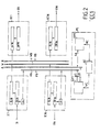
- the control circuit CC1 is represented in Fig. 2 wherein only the first I1/O1 and the last I16/O16 of its input and output terminals respectively and the circuits associated thereto are shown. It includes a 16-bit address bus AB, a 16-bit write bus WB, a 16-bit read bus RB and a 4-bit pointer bus PB to transfer digital signals and of which AB, WB and RB are connected to the respective terminals A, W and R mentioned above, whilst PB is an internal bus to transfer relative addresses of transmitter circuits TC1/TC16 as will be described below.
- the terminals I1 to I16 of the control circuit CC1 are coupled to the busses WB and PB via respective input circuits IC1 to IC16, whilst the bus RB is coupled to the terminals O1 to O16 of CC1 via output circuits OC1 to OC16.
- Each input circuit IC1/IC16 includes a 16-bit shift register IR16 to which the corresponding input terminal I1/I16 is connected and which is able to store the sub-packets incoming from the corresponding receiver circuit RC1/RC16. When the shift register IR16 is full, the sub-packet stored therein is transferred to a 16-bit latch circuit IL16 also included in each input circuit IC1/IC16.
- This sub-packet remains in the latch circuit IL16 until the write bus WB is ready to transfer it to the sub-memory M1 wherein it will be loaded at a location indicated by the data then present on the pointer bus Pb. These latter data are obtained in the following way.
- the first 4 bits of the sub-packet stored in the shift register IR16 are also transferred to a 4-bit latch circuit L4 also forming part of each input circuit IC1/IC16. From there, these 4 bits are transferred to a pointer control circuit PC included in CC1 and more particularly to a write pointer table WPT thereof via a terminal WT.
- the write pointer table WPT contains for each of the 16 storage areas of the sub-memory M1 a write pointer indicating the address of the next free location in that storage area, i.e. where the sub-packet should be loaded.
- the first 4 bits indicate the number 1 to 16 of the storage area of the sub-memory M1 allocated to the destination transmitter circuit TC1/TC16, i.e. the relative address 1 to 16 of this transmitter circuit, whilst the 12 remaining bits indicate the next free location 1 to 4,O96 (4K) in this storage area wherein the 16-bit sub-packet can be stored.
- This 16-bit address is then transmitted to the address bus AB via a terminal WA of the write pointer table WPT and so to the 16 address lines via the address terminal A of the control circuit CC1.
- This address is then indicated simultaneously to the 8 sub-memories M1 to M8 which are handled in parallel and wherein the sub-packets coming from the 8 control circuits CC1 to CC8 are thus loaded in homologous locations.
- the contents of the 4-bit latch circuits L4 of the 16 input circuits IC1 to IC16 are successively transferred to the write pointer table WPT via the pointer bus PB and the terminal WT.
- a 16-bit corresponding address is then generated by the write pointer table WPT, is loaded on the address bus AB and appears on the address terminal A of the control circuit CC1.
- the contents of the latch circuits IL16 of the corresponding input circuits IC1/IC16 of the 8 control circuits CC1 to CC8 are loaded on the write bus WB thereof and appear at their write terminals W.
- the 8 sub-packets are then transferred to the corresponding sub-memories M1 to M8 at homologous locations.
- the sub-memories M1 to M8 are unloaded by the control circuits CC1 to CC8.
- This unloading operation of the sub-memories M1 to M8 is performed under the control of a read pointer table RPT included in the pointer control circuit PC of the control circuit CC1.
- the read pointer table RPT contains for each transmitter circuit TC1/TC16 a read pointer indicating for the corresponding storage area the location of the sub-packet to be unloaded.
- the read pointer table RPT loads successively for each transmitter circuit TC1/TC16 a 16-bit address on the address bus AB via a terminal RA. This 16-bit address, obtained in a similar way as the one mentioned above, is transferred to all the sub-memories M1 to M8 via the address terminal A of the control circuit CC1.
- the sub-packets contained in the sub-memories M1 to M8 are transferred through the 16 read lines connected to the read terminals R of the corresponding control circuits CC1 to CC8 and so on their respective read busses RB.
- the sub-packets are then transferred to the output circuits OC1/OC16 corresponding to the selected transmitter circuit TC1/TC16. More particularly, each sub-packet is loaded in a 16-bit latch circuit OL16 included in each output circuit OC1/OC16 of each control circuit CC1 to CC8.
- the sub-packet is transferred to a 16-bit shift register OR16 also included in the output circuits OC1 to OC16 and from which it is sent to the destination transmitter circuit TC1/TC16 via the corresponding terminal O1/O16.
- the pointer control circuit PC of the control circuit CC1 further includes a queue control circuit QC coupled to the write pointer table WPT via a terminal WC and to the read pointer table RPT via a terminal RC.
- the purpose of this queue control circuit QC is to compare the values of the write pointer and of the read pointer of each storage area of the sub-memory M1 and thus in this way of the sub-memories M2 to M8 in order to detect empty or full storage areas and to take the appropriate decisions. For instance, in case of an empty storage area corresponding to a particular transmitter circuit TC1/TC16, a so-called synchronization packet may be generated and transferred to this circuit.
- the 16-bit write and read addresses are identical for the 8 sub-memories M1 to M8 and are generated by the control circuit CC1, the 4-bit latch circuit L4 of the input circuits IC1 to IC16, the pointer bus PB, the pointer control circuit PC and the address bus AB as well as its address terminal A are only present in this control circuit CC1 and not in the other control circuits CC2 to CC8.
- the subdivision of the memory MM into 8 sub-memories M1 to M8 which are themselves subdivided into 16 storage areas each associated to a transmitter circuit TC1/TC16 has the advantage of being easy to implement and of avoiding interactions between digital signals belonging to packets intended for different transmitter circuits TC1 to TC16.
- the congestion on one transmitter circuit TC1/TC16 due for instance to an overflow of its storage area, does not affect the operation of the other transmitter circuits.
- the storage areas and thus also the whole memory MM are generally over-dimensioned so that the size of the memory MM is larger than the one required for a particular application.
- One solution to this congestion problem consists in using the memory MM as a common pool wherein the space reserved for each transmitter circuit TC1/TC16 may be dynamically allocated. However this would require additional control functions to load and unload the memory MM. Also broadcasting packets to a fixed number of transmitter circuits TC1 to TC16 would require an especially dedicated part of the memory MM wherein the packets remain stored until all the transmitter circuits TC1 to TC16 participating in the broadcast connection have read them. Also here additional control functions would be necessary. Furthermore, it is obvious that in these two last cases the memory MM could no longer be subdivided into identical sub-memories such as M1 to M8.
- the memory MM should be separate from the chip of the switching system since its size may then be independently adapted to the application.
- the memory MM is no longer necessary when the bitrate at which the packets are transmitted by the transmitter circuits TC1 to TC16 via their respective output terminals T1 to T16 is sufficiently high to follow the rhythm at which these packets are received from the receiver circuits RC1 to RC16.
Landscapes
- Engineering & Computer Science (AREA)
- Computer Networks & Wireless Communication (AREA)
- Signal Processing (AREA)
- Data Exchanges In Wide-Area Networks (AREA)
Claims (11)
- Durchschalteanlage (SW) mit:- einer Anzahl von Eingangsklemmen (R1-R16), die mit Empfangsmitteln (RC1-RC16) verbunden sind, die diese Pakete von digitalen Signalen empfangen und jedes dieser Pakete in eine Anzahl (8) von Teilpaketen unterteilen können;- Steuermitteln (CC1-CC8), an welche mindestens ein eine Leitweginformation enthaltendes Teilpaket jedes dieser Pakete angelegt wird;- einer Anzahl von den entsprechenden Teilpaketen jedes dieser Pakete zugeordneten Speichern (M1-M8), wobei die genannten Teilpakete unter der Steuerung der genannten Steuermittel in die Speicher eingeschrieben und ausgelesen werden;- Sendemitteln (TC1-TC16), welche mit einer Anzahl von Ausgangsklemmen (T1-T16) verbunden sind und an welche die ausgelesenen Teilpakete angelegt werden, wobei die genannten Sendemittel in der Lage sind, aus ihren Teil-paketen ein Paket neu zusammenzustellen und dieses neu zusammengestellte Paket an mindestens eine durch die genannte Leitweginformation angegebene Klemme zu übermitteln, dadurch gekennzeichnet, dass jeder der genannten Speicher (M1-M8) in eine Anzahl (16) von Speicherzonen aufgeteilt ist, welche entsprechenden der Ausgangsklemmen (T1-T16) zugeordnet sind, und das die genannten Steuermittel unter der Steuerung der genannten Leit-weginformation die Teilpakete eines an die genannte angegebene Ausgangsklemme zu übermittelnden Paketes in die ihr zugeordnete Speicherzone einschreiben.
- Durchschalteanlage nach Anspruch 1, dadurch gekennzeichnet, dass die genannten Steuermittel (CC1-CC8) eine erste Steuerschaltung (CC1) aufweisen, an welche das genannte eine, die Leitweginformation enthaltende Teilpaket von den genannten Empfängernmitteln (RC1-RC16) angelegt wird, und weiter eine Anzahl von zweiten Steuerschaltungen (CC2-CC8), an welche die verbleibenden Teilpakete eines Paketes von den genannten Empfängermitteln (RC1-RC16) angelegt werden.
- Durchschalteanlage nach Anspruch 2, dadurch gekennzeichnet, dass die genannte erste Steuerschaltung (CC1) einem (M1) der genannten Speicher (M1-M8) zugeordnet ist, und dass jede der zweiten Steuerschaltungen (CC2-CC8) einem entsprechenden Speicher (M2-M8) der genannten Anzahl von Speichern zugeordnet ist.
- Durchschalteanlage nach Anspruch 1, dadurch gekennzeichnet, dass die genannte Anzahl von Speichern (M1-M8) auf einen Chip angeordnet ist, welcher von den andern Schaltungen des Durchschaltesystems (SW) getrennt ist.
- Durchschalteanlage nach Anspruch 1, dadurch gekennzeichnet, dass die genannte Anzahl von Teilpaketen eines Paketes gleichzeitig und in homologer Art in die entsprechenden Speicherzonen eingeschrieben und ausgelesen wird.
- Durchschalteanlage (SW) nach Anspruch 1, dadurch gekennzeichnet, dass die genannten Empfängermittel (RC1-RC16) eine Anzahl von Empfängerschaltungen (RC1/16) aufweisen, mit welchen je eine Eingangsklemme (R1/16) verbunden ist und welche in der Lage sind, ein von einer angeschlossenen Eingangsklemme erhaltenes Paket in die genannte Anzahl von Teilpaketen zu unterteilen.
- Durchschalteanlage nach Anspruch 2 und 6, dadurch gekennzeichnet, dass die genannten ersten (CC1) und zweiten (CC2-CC8) Steuerschaltungen je eine Anzahl (16) von Eingangszwischenspeichermitteln (IL16) aufweisen, welche je in der Lage sind, ein von der genannten Empfängerschaltung (RC1-RC16) erhaltenes Teilpaket zu halten, bevor es in die Speicherzone eingeschrieben wird, welche der gewünschten Ausgangsklemme (T1/16) entspricht.
- Durchschalteanlage nach Anspruch 7, dadurch gekennzeichnet, dass die erste Steuerschaltung (CC1) Adressiermittel (L4, PB, PC, AB) aufweist, die in der Lage sind, aus der im genannten einen daran angelegten Teilpaket, welches die Leitweginformation enthält, die Adresse der gewünschten Ausgangsklemme (P1/16) zu entnehmen und der genannten Anzahl von Speichern (M1-M8) den Speicherplatz der entsprechenden homologen Speicherzone anzugeben, in welche die Teilpakete eines in den entsprechenden Eingangszwischenspeichermitteln (IL16) gespeicherten Paketes einzuschreiben sind.
- Durchschalteanlage nach Anspruch 8, dadurch gekennzeichnet, dass die genannten Adressiermittel (L4, PD, PC, AB) in der Lage sind, der genannten Anzahl von Speichern (M1-M8) den Platz der entsprechenden homologen Speicherzone anzugeben, aus welcher die Teilpakete eines Paketes auszulesen und an die entsprechenden Ausgangszwischenspeichermittel (0L16) zu transferieren sind.
- Durchschalteanlage nach Anspruch 1, dadurch gekennzeichnet, dass die genannten Sendemittel(TC1 bis TC16) eine Anzahl von Sendeschaltungen (TC1-TC16) aufweisen, die je mit einer entsprechenden Ausgangsklemme (T1/16) gekoppelt sind und an welche die Teilpakete eines aus der entsprechenden homologen Speicherzone der genannten Speicher (M1-M8) auszulesenden Paketes angelegt werden und welche in der Lage sind, aus ihren Teilpaketen ein Paket neu aufzubauen.
- Durchschalteanlage nach Anspruch 2 und 1O, dadurch gekennzeichnet, dass die genannten ersten (CC1) und zweiten (CC2-CC8) Steuermittel je eine Anzahl (16) von Ausgangszwischenspeichermitteln (OL16) aufweisen, die je in der Lage sind, ein aus der der gewünschten Ausgangsklemme (T1/16) entsprechenden Speicherzone ausgelesenes Teilpaket zu speichern, bevor es an die entsprechende Sendeschaltung (PC1/16) übertragen wird.
Applications Claiming Priority (2)
| Application Number | Priority Date | Filing Date | Title |
|---|---|---|---|
| BE8700283A BE1000396A7 (fr) | 1987-03-18 | 1987-03-18 | Systeme de commutation. |
| BE8700283 | 1987-03-18 |
Publications (2)
| Publication Number | Publication Date |
|---|---|
| EP0357618A1 EP0357618A1 (de) | 1990-03-14 |
| EP0357618B1 true EP0357618B1 (de) | 1992-10-07 |
Family
ID=3882578
Family Applications (1)
| Application Number | Title | Priority Date | Filing Date |
|---|---|---|---|
| EP19880902469 Expired EP0357618B1 (de) | 1987-03-18 | 1988-03-11 | Vermittlungssystem |
Country Status (5)
| Country | Link |
|---|---|
| EP (1) | EP0357618B1 (de) |
| AU (1) | AU601818B2 (de) |
| BE (1) | BE1000396A7 (de) |
| ES (1) | ES2006601A6 (de) |
| WO (1) | WO1988007298A1 (de) |
Families Citing this family (23)
| Publication number | Priority date | Publication date | Assignee | Title |
|---|---|---|---|---|
| BE1000512A7 (nl) * | 1987-05-07 | 1989-01-10 | Bell Telephone Mfg | Schakelnetwerk. |
| US5268896A (en) * | 1988-03-26 | 1993-12-07 | Alcatel N.V. | Communication switching element |
| AU621315B2 (en) * | 1988-10-03 | 1992-03-12 | Alcatel N.V. | Switching system |
| GB8824972D0 (en) * | 1988-10-25 | 1988-11-30 | Plessey Telecomm | Time division switch |
| EP0422910A3 (en) * | 1989-10-10 | 1991-11-06 | American Telephone And Telegraph Company | High capacity memory based packet switches |
| DE69032498T2 (de) * | 1989-10-23 | 1999-03-04 | Mitsubishi Denki K.K., Tokio/Tokyo | Zellenvermittlungseinrichtung |
| EP0521027A4 (en) * | 1990-03-22 | 1994-10-19 | Australian & Overseas Telecom | Multicasting method for a telecommunications network |
| JP2993715B2 (ja) * | 1990-08-17 | 1999-12-27 | 株式会社日立製作所 | Atmスイッチおよびその制御方法 |
| DE4116939A1 (de) * | 1991-05-24 | 1992-11-26 | Standard Elektrik Lorenz Ag | Koppelfeld zum durchschalten von kanaelen |
| EP0593609A1 (de) * | 1991-07-01 | 1994-04-27 | Telstra Corporation Limited | Vermittlungsarchitektur mit hoher geschwindigkeit |
| AU655308B2 (en) * | 1991-07-01 | 1994-12-15 | Telstra Corporation Limited | High speed switching architecture |
| JP2671699B2 (ja) * | 1991-11-15 | 1997-10-29 | 三菱電機株式会社 | セル交換装置 |
| US5398235A (en) * | 1991-11-15 | 1995-03-14 | Mitsubishi Denki Kabushiki Kaisha | Cell exchanging apparatus |
| US5321691A (en) * | 1993-01-11 | 1994-06-14 | At&T Bell Laboratories | Asynchronous transfer mode (ATM) switch fabric |
| DE69433229T2 (de) * | 1993-02-15 | 2004-08-12 | Mitsubishi Denki K.K. | ATM-Schalter |
| GB2303274B (en) * | 1995-07-11 | 1999-09-08 | Fujitsu Ltd | Switching apparatus |
| GB9617553D0 (en) * | 1996-08-21 | 1996-10-02 | Walker Christopher P H | Communication system with improved routing switch |
| US6016307A (en) | 1996-10-31 | 2000-01-18 | Connect One, Inc. | Multi-protocol telecommunications routing optimization |
| US6473404B1 (en) | 1998-11-24 | 2002-10-29 | Connect One, Inc. | Multi-protocol telecommunications routing optimization |
| JPH11154954A (ja) | 1997-11-20 | 1999-06-08 | Hitachi Ltd | Atmスイッチ |
| GB0031761D0 (en) * | 2000-12-29 | 2001-02-07 | Mitel Semiconductor Ltd | Data queues |
| GB2382899B (en) | 2000-12-29 | 2003-12-17 | Zarlink Semiconductor Ltd | A data queue system |
| US7054311B2 (en) * | 2001-07-27 | 2006-05-30 | 4198638 Canada Inc. | Methods and apparatus for storage and processing of routing information |
Family Cites Families (4)
| Publication number | Priority date | Publication date | Assignee | Title |
|---|---|---|---|---|
| FR2458196A1 (fr) * | 1979-06-01 | 1980-12-26 | Materiel Telephonique | Niveau de commutation d'un operateur pour reseau de commutation de donnees numeriques par paquets |
| FR2538976A1 (fr) * | 1982-12-29 | 1984-07-06 | Servel Michel | Systeme de commutation de paquets synchrones de longueur fixe |
| US4577308A (en) * | 1984-04-06 | 1986-03-18 | At&T Bell Laboratories | Multiplexed interconnection of packet switching node packages |
| BE904100A (fr) * | 1986-01-24 | 1986-07-24 | Itt Ind Belgium | Systeme de commutation. |
-
1987
- 1987-03-18 BE BE8700283A patent/BE1000396A7/fr not_active IP Right Cessation
-
1988
- 1988-03-04 AU AU12628/88A patent/AU601818B2/en not_active Ceased
- 1988-03-11 EP EP19880902469 patent/EP0357618B1/de not_active Expired
- 1988-03-11 WO PCT/EP1988/000212 patent/WO1988007298A1/en not_active Ceased
- 1988-03-18 ES ES8800836A patent/ES2006601A6/es not_active Expired
Also Published As
| Publication number | Publication date |
|---|---|
| AU601818B2 (en) | 1990-09-20 |
| WO1988007298A1 (en) | 1988-09-22 |
| BE1000396A7 (fr) | 1988-11-22 |
| AU1262888A (en) | 1988-09-22 |
| EP0357618A1 (de) | 1990-03-14 |
| ES2006601A6 (es) | 1989-05-01 |
Similar Documents
| Publication | Publication Date | Title |
|---|---|---|
| EP0357618B1 (de) | Vermittlungssystem | |
| AU642830B2 (en) | Multiple virtual fifo arrangement | |
| US4849968A (en) | Buffer management system | |
| AU767085B2 (en) | Optimizing the transfer of data packets between LANs | |
| EP1192753B1 (de) | Verfahren und vorrichtung zur paketvermittlung mittels eines geteilten pufferspeichers | |
| US7782849B2 (en) | Data switch and switch fabric | |
| AU726992B2 (en) | Computer interface for direct mapping of application data | |
| US6147999A (en) | ATM switch capable of routing IP packet | |
| KR100356447B1 (ko) | 메모리인터페이스유닛,공유메모리스위치시스템및관련방법 | |
| EP0778686B1 (de) | ATM-Vermittlungsstelle mit Eingangs- und Ausgangsanschlussstellen | |
| US5099475A (en) | Switching system | |
| EP0471344A1 (de) | Verfahren und Schaltung zur Verkehrsformung | |
| US5649217A (en) | Switching system having control circuit and plural buffer memories for data exchange in asynchronous transfer mode | |
| EP0335848B1 (de) | Datenpaketschaltungsanordnung zum Übertragen von Datenpaketen von einer oder vielen einkommenden Datenübertragungsanlagen zu einer oder vielen ausgehenden Datenübertragungsanlagen | |
| EP1045558A2 (de) | Zeitvielfach (TDM)-Vermittlungssystem mit sehr breitem Speicher | |
| US5210743A (en) | Switching element with multiple operating modes and switching network incorporating a plurality of such switching elements, in particular for switching asynchronous time-division multiplex packets | |
| JP2644023B2 (ja) | コミュニケイションスイッチング素子 | |
| US6553035B1 (en) | Apparatus and method for queuing data | |
| US6314489B1 (en) | Methods and systems for storing cell data using a bank of cell buffers | |
| JP3133234B2 (ja) | Atmスイッチのアドレス生成回路 | |
| US6301259B1 (en) | Switch and switching method | |
| US7116659B2 (en) | Data transmission memory | |
| US4251684A (en) | Data storage systems | |
| NZ223781A (en) | Packet switching network: packets divided on receipt and rebuilt on transmission | |
| EP0226688B1 (de) | Serieller Verbindungsadapter für eine Übertragungssteuereinrichtung |
Legal Events
| Date | Code | Title | Description |
|---|---|---|---|
| PUAI | Public reference made under article 153(3) epc to a published international application that has entered the european phase |
Free format text: ORIGINAL CODE: 0009012 |
|
| 17P | Request for examination filed |
Effective date: 19890912 |
|
| AK | Designated contracting states |
Kind code of ref document: A1 Designated state(s): BE CH IT LI |
|
| 17Q | First examination report despatched |
Effective date: 19920324 |
|
| GRAA | (expected) grant |
Free format text: ORIGINAL CODE: 0009210 |
|
| AK | Designated contracting states |
Kind code of ref document: B1 Designated state(s): BE CH IT LI |
|
| PG25 | Lapsed in a contracting state [announced via postgrant information from national office to epo] |
Ref country code: BE Effective date: 19921007 |
|
| ITF | It: translation for a ep patent filed | ||
| PGFP | Annual fee paid to national office [announced via postgrant information from national office to epo] |
Ref country code: CH Payment date: 19930617 Year of fee payment: 6 |
|
| PLBE | No opposition filed within time limit |
Free format text: ORIGINAL CODE: 0009261 |
|
| STAA | Information on the status of an ep patent application or granted ep patent |
Free format text: STATUS: NO OPPOSITION FILED WITHIN TIME LIMIT |
|
| 26N | No opposition filed | ||
| PG25 | Lapsed in a contracting state [announced via postgrant information from national office to epo] |
Ref country code: LI Effective date: 19940331 Ref country code: CH Effective date: 19940331 |
|
| REG | Reference to a national code |
Ref country code: CH Ref legal event code: PL |
|
| PG25 | Lapsed in a contracting state [announced via postgrant information from national office to epo] |
Ref country code: IT Free format text: LAPSE BECAUSE OF NON-PAYMENT OF DUE FEES;WARNING: LAPSES OF ITALIAN PATENTS WITH EFFECTIVE DATE BEFORE 2007 MAY HAVE OCCURRED AT ANY TIME BEFORE 2007. THE CORRECT EFFECTIVE DATE MAY BE DIFFERENT FROM THE ONE RECORDED. Effective date: 20050311 |