EP0357815A1 - Source de courant constant commutable pour portes I2L - Google Patents
Source de courant constant commutable pour portes I2L Download PDFInfo
- Publication number
- EP0357815A1 EP0357815A1 EP88114531A EP88114531A EP0357815A1 EP 0357815 A1 EP0357815 A1 EP 0357815A1 EP 88114531 A EP88114531 A EP 88114531A EP 88114531 A EP88114531 A EP 88114531A EP 0357815 A1 EP0357815 A1 EP 0357815A1
- Authority
- EP
- European Patent Office
- Prior art keywords
- gates
- current source
- constant current
- current
- output
- Prior art date
- Legal status (The legal status is an assumption and is not a legal conclusion. Google has not performed a legal analysis and makes no representation as to the accuracy of the status listed.)
- Withdrawn
Links
- 230000001105 regulatory effect Effects 0.000 abstract description 4
- 230000003321 amplification Effects 0.000 description 9
- 238000003199 nucleic acid amplification method Methods 0.000 description 9
- 238000002347 injection Methods 0.000 description 4
- 239000007924 injection Substances 0.000 description 4
- 230000002349 favourable effect Effects 0.000 description 3
- 239000004065 semiconductor Substances 0.000 description 3
- 230000015556 catabolic process Effects 0.000 description 2
- 238000010586 diagram Methods 0.000 description 2
- 230000000694 effects Effects 0.000 description 2
- 238000002955 isolation Methods 0.000 description 2
- XUIMIQQOPSSXEZ-UHFFFAOYSA-N Silicon Chemical compound [Si] XUIMIQQOPSSXEZ-UHFFFAOYSA-N 0.000 description 1
- 238000009776 industrial production Methods 0.000 description 1
- 238000009413 insulation Methods 0.000 description 1
- 239000012212 insulator Substances 0.000 description 1
- 238000004519 manufacturing process Methods 0.000 description 1
- 230000010355 oscillation Effects 0.000 description 1
- 229910052710 silicon Inorganic materials 0.000 description 1
- 239000010703 silicon Substances 0.000 description 1
- 230000006641 stabilisation Effects 0.000 description 1
- 238000011105 stabilization Methods 0.000 description 1
- 230000003068 static effect Effects 0.000 description 1
Images

Classifications
-
- H—ELECTRICITY
- H03—ELECTRONIC CIRCUITRY
- H03K—PULSE TECHNIQUE
- H03K19/00—Logic circuits, i.e. having at least two inputs acting on one output; Inverting circuits
- H03K19/02—Logic circuits, i.e. having at least two inputs acting on one output; Inverting circuits using specified components
- H03K19/08—Logic circuits, i.e. having at least two inputs acting on one output; Inverting circuits using specified components using semiconductor devices
- H03K19/082—Logic circuits, i.e. having at least two inputs acting on one output; Inverting circuits using specified components using semiconductor devices using bipolar transistors
- H03K19/091—Integrated injection logic or merged transistor logic
-
- G—PHYSICS
- G05—CONTROLLING; REGULATING
- G05F—SYSTEMS FOR REGULATING ELECTRIC OR MAGNETIC VARIABLES
- G05F1/00—Automatic systems in which deviations of an electric quantity from one or more predetermined values are detected at the output of the system and fed back to a device within the system to restore the detected quantity to its predetermined value or values, i.e. retroactive systems
- G05F1/10—Regulating voltage or current
- G05F1/46—Regulating voltage or current wherein the variable actually regulated by the final control device is DC
- G05F1/462—Regulating voltage or current wherein the variable actually regulated by the final control device is DC as a function of the requirements of the load, e.g. delay, temperature, specific voltage/current characteristic
Definitions
- the present invention relates to switchable constant current sources in the form of monolithically integrated circuits according to the preamble of patent claim 1.
- I2L technology Integrated Injection Logic
- inverter circuits flip-flops, counters, etc.
- An I2L gate usually only requires one insulator trough on the semiconductor chip and, if several I2L gates of the same type are built, the injector inputs of all I2L gates can be supplied by simply connecting them in parallel via a unique current injection.
- I2L gates are, inter alia, from the journal IEEE Journal Of Solid-State Circuits, Vol. SC-12, No. 5, October 1977 from the article "Electrical Parameters, Static and Dynamic Response of I2L” by Teunis Poorter, pages 440 to 449 and the article "Theshold I2L and Its Applications to Binary Symmetric Functions and Multivalued Logic” by T. Tich Dao, pages 463 to 472 and from the journal IEEE Journal Of Solid-State Circuits, Vol. SC-14, No. 1, February 1979 from the article "A Single-Chip I2L PCM Codec" by R.A. Blauschild et al, pages 59 to 64.
- FIG. 1B A typical I2L gate is shown in FIG. 1B.
- the I2L gate shown in FIG. 1B has a control input E which can be acted upon by a control signal, an injector input Inj which is connected to the current input of a first transistor Ti of one type, here to the emitter of a pnp transistor and to one impressed current I Inj is applied and a plurality of outputs, here two outputs A1, A2, each of which is connected to its own collector electrode, acting as a collector, of an output transistor Ta of the inverse type to the transistor Ti, here an npn transistor.
- the output transistor Ta requires several collectors as outputs, it is implemented by a reversely operated multiemitter transistor.
- the base terminal of the first transistor Ti and the collector terminal of the output transistor Ta, which acts as an emitter, are both connected to a fixed potential, preferably the reference potential.
- the current output of the first transistor Ti, here the collector terminal, together with the base terminal of the output transistor Ta forms the control input E of the I2L gate. If, as shown in FIGS. 1A and 1B, a current output, here the current output A1, is connected to the control input E, a current mirror circuit IB with the resulting circuit structure is obtained, as shown in FIG. 2 as a discretely constructed current mirror circuit IC.
- I2L gates an inversely operated multi-emitter transistor is used as the output transistor Ta.
- Usual transistors are characterized by a very small current gain B inv in reverse operation.
- I2L gates Advantages of such current sources implemented by I2L gates are that they are very small, that several such current sources implemented on a chip only require a common current impression as a reference current source and that they can be easily switched on or off by varying the potential present at signal input E.
- each individual one of these current source circuits requires its own current impression ID, which provides the reference current I Inj ' .
- the circuit node designated A1 'in FIG. 2 corresponds in its effect em in FIGS. 1A and 1B to the circuit node formed by the control input E and the current output A1.
- the object of the invention is to provide a switchable constant current source in the form of a monolithically integrable electronic circuit with the smallest possible chip area requirement, in which there is a fixed relationship between a predeterminable electrical variable and the current source output current over a longer period of time even in the case of large series production.
- the invention is based on the fact that several I2L gates, which are produced in the same operation on a chip, have almost identical technical data, such as current amplification factor or input impedances. If, for example, several I2L gates are interconnected to form a circuit node and this circuit node is subjected to a total injector current, this total injector current is distributed equally among all injector inputs connected to this node.
- I2L gates are connected together with their injector inputs to form a circuit node and the injector total current impressed on this circuit node as a manipulated variable of a control loop is controlled in such a way that one of these I2L gates, which is provided as a reference gate, is used as a controlled system, the corresponding one at its injector input Part of said manipulated variable is fed in and its output current is compared with a reference variable and the resulting control difference controls a control amplifier, the output currents of the other I2L gates are quasi-controlled constant.
- FIG. 3 shows as a basic circuit diagram a switchable constant current source according to the invention with two identically constructed I2L gates G1 and G2, the injector inputs INJ1 and INJ2 of which together form a first circuit node K1.
- a switchable constant current source according to the invention requires at least two I2L gates, but almost any number of I2L gates can also be provided, each of which is interconnected with its injector inputs.
- a current output AI1 of the first I2L gate G1 is connected to an input of a comparator device VE, which compares the output current I G1 of this first I2L gate with a reference variable, in particular a reference current I Ref , and whose output variable controls a control amplifier RV, the output variable this control amplifier corresponds to the injector total current I E as a manipulated variable and is impressed on the first circuit node K1.
- a comparator device VE which compares the output current I G1 of this first I2L gate with a reference variable, in particular a reference current I Ref , and whose output variable controls a control amplifier RV, the output variable this control amplifier corresponds to the injector total current I E as a manipulated variable and is impressed on the first circuit node K1.
- this total injector current I E is distributed equally to all injector inputs connected to this first circuit node K1.
- an injector current is impressed on each injector input that is half as large as the total injector current I E.
- the output current of the I2L gate not switched as a reference gate that is to say the I2L gate G2 in FIG. 2, is provided as the output current of the switchable constant current source and can be switched as a function of the control input E2 of this I2L gate G2.
- FIG 4 shows an exemplary embodiment of a switchable constant current source according to the invention, a circuit formed from five identically constructed I2L gates G1, G2, G3, G4, G5, the injector inputs Inj1, Inj2, ... of which are connected together to a first circuit node K1.
- I2L gates with two current outputs AI1a, AI1b, AI2a, AI2b, AI3a, ... are provided, so that a total of eight current outputs AI2a, AI2b, ..., AI5b of the switchable constant current source are available, which can be switched in pairs depending on the potential applied to the control inputs E2, E3, E4 and E5.
- a current output AI1a of the first I2L gate G1 is connected to the inverting input of an operational amplifier OP with differential amplifier input and at the same time via a resistor Rg to the supply potential U B.
- the non-inverting input of this operational amplifier OP is connected to a current injection IR and connected to the supply potential U B via a resistor Ri.
- the operational amplifier OP provides the total injector current I E at its output, which is connected to the first circuit node K1.
- the current of the current output AI1a of the first I2L gate G1 which is fed back to the operational amplifier input, is regulated in such a way that it is of the same size as the reference current I Ref . Due to the matching behavior of all I2L gates G1, G2, ... G5 contained in this constant current source, the output currents at the other current outputs AI1b, AI2a, AI2b, ... of the I2L gates G1, G2, ... are also as large like the reference current I Ref .
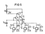
- FIG. 5 shows a particularly advantageous embodiment of a switchable constant current source according to the invention with three identically constructed I2L gates G1, G2 and G3.
- the number of these I2L gates is largely arbitrary and depends only on the requirements placed on the switchable constant current source.
- the I2L gates G1, G2 and G3 shown in FIG. 5 each have a control input E1, E2 and E3, an injector input Inj 1, Inj 2 and Inj 3 and two switchable current outputs AI1a, AI1b, AI2a, AI2b, AI3a and AI3b.
- the number of current outputs of each I2L gate is also arbitrary and only depends on the requirements for the switchable constant current source.
- the current outputs AI2a, AI2b, AI3a and AI3b the I2L gates G2 and G3 are provided as current outputs of the switchable constant current source and can be switched via a corresponding potential applied to the control inputs E2 and E3 of these I2L gates.
- the first current output AI1a of the first I2L gate G1 provided as a reference gate is connected to the emitter terminal of a transistor Tk
- the second current output AI1b of this first I2L gate G1 is connected in the same way to the emitter of a further transistor Tk '.
- the collector terminal of the transistor Tk forms a second circuit node K2 with the base terminal of a transistor T1 and the current output of a reference current source IK.
- the emitter terminal of the transistor T1 is connected to the base terminal of a transistor T2 and to the collector terminal of the transistor Tk '.
- the collector connections of the transistors T1 and T2 connected as a Darlington stage are connected together to the supply potential U B.
- the emitter connection of the transistor T2 is connected to a first circuit node K1 via a resistor Re.
- the injector inputs Inj1, Inj2 and Inj3 of all I2L gates G1, G2 and G3 are also connected to this first circuit node K1.
- the base connections of the transistors Tk and Tk ' are connected to a constant potential U K.
- the control circuit used in FIG. 5 is very simple.
- the output current of the first I2L gate G1 provided as a reference gate is compared in a second circuit node K2 with the reference current I Ref provided by a constant current source IK.
- the base connection of the transistor T1 serving as a control amplifier is also connected to this second circuit node K2, whose emitter current could in principle be impressed directly on the first circuit node K1 as the total injector current.
- the control amplifier transistor T1 should have a current amplification factor that is as large as possible in order to keep this fault current as small as possible. That's why he's going through another Transistor T2 added to a Darlington transistor with a high current amplification factor.
- Such a resistance is also recommended in other embodiments of switchable constant current sources according to the invention.
- the emitter of the input transistor T1 of the Darlington stage is not only connected to the base of the output transistor T2 of the Darlington stage, but also to the reference potential via a constant current source. Since the I2L gates G1, G2, ... used in the constant current source shown in FIG. 5 each have two current outputs AI1a, AI1b, AI2a, ..., however, only the current of an output AI1a from the first I2L gate provided as a reference gate is required as the actual value for the control, it proves to be advantageous to switch the other current output AI1b of this I2L gate G1 to stabilize the Darlington circuit to the emitter of the transistor T1.
Landscapes
- Engineering & Computer Science (AREA)
- Physics & Mathematics (AREA)
- Power Engineering (AREA)
- Computer Hardware Design (AREA)
- Computing Systems (AREA)
- General Engineering & Computer Science (AREA)
- Mathematical Physics (AREA)
- Electromagnetism (AREA)
- General Physics & Mathematics (AREA)
- Radar, Positioning & Navigation (AREA)
- Automation & Control Theory (AREA)
- Control Of Electrical Variables (AREA)
Priority Applications (1)
| Application Number | Priority Date | Filing Date | Title |
|---|---|---|---|
| EP88114531A EP0357815A1 (fr) | 1988-09-06 | 1988-09-06 | Source de courant constant commutable pour portes I2L |
Applications Claiming Priority (1)
| Application Number | Priority Date | Filing Date | Title |
|---|---|---|---|
| EP88114531A EP0357815A1 (fr) | 1988-09-06 | 1988-09-06 | Source de courant constant commutable pour portes I2L |
Publications (1)
| Publication Number | Publication Date |
|---|---|
| EP0357815A1 true EP0357815A1 (fr) | 1990-03-14 |
Family
ID=8199275
Family Applications (1)
| Application Number | Title | Priority Date | Filing Date |
|---|---|---|---|
| EP88114531A Withdrawn EP0357815A1 (fr) | 1988-09-06 | 1988-09-06 | Source de courant constant commutable pour portes I2L |
Country Status (1)
| Country | Link |
|---|---|
| EP (1) | EP0357815A1 (fr) |
Cited By (3)
| Publication number | Priority date | Publication date | Assignee | Title |
|---|---|---|---|---|
| EP0505755A3 (en) * | 1991-03-25 | 1993-04-28 | Motorola, Inc. | Current biasing for i2l circuits |
| RU2172064C2 (ru) * | 1999-11-04 | 2001-08-10 | Бубенников Александр Николаевич | Микромощный логический элемент с высокой нагрузочной способностью |
| EP3260117B1 (fr) | 2003-09-12 | 2019-04-17 | Amgen, Inc | Formulation à dissolution rapide de cinacalcet hcl |
Citations (1)
| Publication number | Priority date | Publication date | Assignee | Title |
|---|---|---|---|---|
| GB2030810A (en) * | 1978-08-28 | 1980-04-10 | Philips Nv | Integated injection logic circuit |
-
1988
- 1988-09-06 EP EP88114531A patent/EP0357815A1/fr not_active Withdrawn
Patent Citations (1)
| Publication number | Priority date | Publication date | Assignee | Title |
|---|---|---|---|---|
| GB2030810A (en) * | 1978-08-28 | 1980-04-10 | Philips Nv | Integated injection logic circuit |
Non-Patent Citations (1)
| Title |
|---|
| IBM TECHNICAL DISCLOSURE BULLETIN, Band 18, Nr. 4, September 1975, Seiten 1220-1222, New York, US; R.C. JAEGER: "Regulated power supply for MTL integrated circuits" * |
Cited By (3)
| Publication number | Priority date | Publication date | Assignee | Title |
|---|---|---|---|---|
| EP0505755A3 (en) * | 1991-03-25 | 1993-04-28 | Motorola, Inc. | Current biasing for i2l circuits |
| RU2172064C2 (ru) * | 1999-11-04 | 2001-08-10 | Бубенников Александр Николаевич | Микромощный логический элемент с высокой нагрузочной способностью |
| EP3260117B1 (fr) | 2003-09-12 | 2019-04-17 | Amgen, Inc | Formulation à dissolution rapide de cinacalcet hcl |
Similar Documents
| Publication | Publication Date | Title |
|---|---|---|
| DE2555297C2 (de) | Digitalschaltung mit Feldeffekttransistoren | |
| EP0096944B1 (fr) | Circuit avec plusieurs chemins de signaux formés par des composants actifs | |
| EP0483537B1 (fr) | Circuit de source de courant | |
| DE3713107C2 (de) | Schaltung zur Erzeugung von konstanten Spannungen in CMOS-Technologie | |
| DE1948850A1 (de) | Differenzverstaerker | |
| DE3713376A1 (de) | Komparator mit erweitertem eingangsgleichtaktspannungsbereich | |
| DE1901804A1 (de) | Stabilisierter Differentialverstaerker | |
| DE69020748T2 (de) | Differenzverstärker mit Spannungsverschiebung zur Erzielung einer Eingangsfähigkeit über den ganzen, sehr niedrigen Versorgungsspannungsbereich. | |
| DE69128596T2 (de) | Transkonduktanzstufe mit breitem dynamischen Bereich | |
| DE3937501A1 (de) | Verfahren und vorrichtung zur erzeugung einer vorspannung | |
| DE69317521T2 (de) | Eingangsschaltung für eine integrierte Schaltung | |
| DE2416534A1 (de) | Komplementaer-symmetrische verstoerkerschaltung | |
| DE68923334T2 (de) | Stromschalterlogikschaltung mit gesteuerten Ausgangssignalpegeln. | |
| DE3528550C2 (fr) | ||
| DE2426447C2 (de) | Komplementäre Transistorschaltung zur Durchführung boole'scher Verknüpfungen | |
| DE69707940T2 (de) | Ruhestromeinstellung für Verstärkerausgangsstufe | |
| DE2520890A1 (de) | Transistorverstaerker der darlington- bauart mit interner vorspannung | |
| DE2924171C2 (fr) | ||
| DE3545392A1 (de) | Stromspiegelschaltung | |
| DE69718122T2 (de) | Verstärkungsregelungsschaltung und Verstärkungsregelungsverfahren | |
| EP0237086B1 (fr) | Circuit de miroir de courant | |
| DE69615638T2 (de) | Spannungsverstärker mit grossen dynamischen Bereich und A/D-Konverter damit | |
| DE2231931C3 (de) | Verstärkerschaltung mit komplementärsymmetrischen Transistoren | |
| DE69427479T2 (de) | Hochgenauer Stromspiegel für niedrige Versorgungsspannung | |
| DE69410662T2 (de) | Referenzstromsgeneratorschaltung |
Legal Events
| Date | Code | Title | Description |
|---|---|---|---|
| PUAI | Public reference made under article 153(3) epc to a published international application that has entered the european phase |
Free format text: ORIGINAL CODE: 0009012 |
|
| AK | Designated contracting states |
Kind code of ref document: A1 Designated state(s): AT BE CH DE ES FR GB GR IT LI LU NL SE |
|
| RBV | Designated contracting states (corrected) |
Designated state(s): DE |
|
| STAA | Information on the status of an ep patent application or granted ep patent |
Free format text: STATUS: THE APPLICATION IS DEEMED TO BE WITHDRAWN |
|
| 18D | Application deemed to be withdrawn |
Effective date: 19900915 |