EP0358098A2 - Régulateur à commutation de tension à gain stabilisé - Google Patents
Régulateur à commutation de tension à gain stabilisé Download PDFInfo
- Publication number
- EP0358098A2 EP0358098A2 EP89115966A EP89115966A EP0358098A2 EP 0358098 A2 EP0358098 A2 EP 0358098A2 EP 89115966 A EP89115966 A EP 89115966A EP 89115966 A EP89115966 A EP 89115966A EP 0358098 A2 EP0358098 A2 EP 0358098A2
- Authority
- EP
- European Patent Office
- Prior art keywords
- voltage
- waveform
- output
- oscillator
- signal
- Prior art date
- Legal status (The legal status is an assumption and is not a legal conclusion. Google has not performed a legal analysis and makes no representation as to the accuracy of the status listed.)
- Granted
Links
Images




Classifications
-
- H—ELECTRICITY
- H03—ELECTRONIC CIRCUITRY
- H03K—PULSE TECHNIQUE
- H03K17/00—Electronic switching or gating, i.e. not by contact-making and –breaking
- H03K17/51—Electronic switching or gating, i.e. not by contact-making and –breaking characterised by the components used
- H03K17/56—Electronic switching or gating, i.e. not by contact-making and –breaking characterised by the components used by the use, as active elements, of semiconductor devices
- H03K17/60—Electronic switching or gating, i.e. not by contact-making and –breaking characterised by the components used by the use, as active elements, of semiconductor devices the devices being bipolar transistors
- H03K17/66—Switching arrangements for passing the current in either direction at will; Switching arrangements for reversing the current at will
- H03K17/665—Switching arrangements for passing the current in either direction at will; Switching arrangements for reversing the current at will connected to one load terminal only
-
- H—ELECTRICITY
- H02—GENERATION; CONVERSION OR DISTRIBUTION OF ELECTRIC POWER
- H02M—APPARATUS FOR CONVERSION BETWEEN AC AND AC, BETWEEN AC AND DC, OR BETWEEN DC AND DC, AND FOR USE WITH MAINS OR SIMILAR POWER SUPPLY SYSTEMS; CONVERSION OF DC OR AC INPUT POWER INTO SURGE OUTPUT POWER; CONTROL OR REGULATION THEREOF
- H02M3/00—Conversion of DC power input into DC power output
- H02M3/02—Conversion of DC power input into DC power output without intermediate conversion into AC
- H02M3/04—Conversion of DC power input into DC power output without intermediate conversion into AC by static converters
- H02M3/10—Conversion of DC power input into DC power output without intermediate conversion into AC by static converters using discharge tubes with control electrode or semiconductor devices with control electrode
- H02M3/145—Conversion of DC power input into DC power output without intermediate conversion into AC by static converters using discharge tubes with control electrode or semiconductor devices with control electrode using devices of a triode or transistor type requiring continuous application of a control signal
- H02M3/155—Conversion of DC power input into DC power output without intermediate conversion into AC by static converters using discharge tubes with control electrode or semiconductor devices with control electrode using devices of a triode or transistor type requiring continuous application of a control signal using semiconductor devices only
- H02M3/156—Conversion of DC power input into DC power output without intermediate conversion into AC by static converters using discharge tubes with control electrode or semiconductor devices with control electrode using devices of a triode or transistor type requiring continuous application of a control signal using semiconductor devices only with automatic control of output voltage or current, e.g. switching regulators
-
- H—ELECTRICITY
- H02—GENERATION; CONVERSION OR DISTRIBUTION OF ELECTRIC POWER
- H02M—APPARATUS FOR CONVERSION BETWEEN AC AND AC, BETWEEN AC AND DC, OR BETWEEN DC AND DC, AND FOR USE WITH MAINS OR SIMILAR POWER SUPPLY SYSTEMS; CONVERSION OF DC OR AC INPUT POWER INTO SURGE OUTPUT POWER; CONTROL OR REGULATION THEREOF
- H02M3/00—Conversion of DC power input into DC power output
- H02M3/22—Conversion of DC power input into DC power output with intermediate conversion into AC
- H02M3/24—Conversion of DC power input into DC power output with intermediate conversion into AC by static converters
- H02M3/28—Conversion of DC power input into DC power output with intermediate conversion into AC by static converters using discharge tubes with control electrode or semiconductor devices with control electrode to produce the intermediate AC
- H02M3/325—Conversion of DC power input into DC power output with intermediate conversion into AC by static converters using discharge tubes with control electrode or semiconductor devices with control electrode to produce the intermediate AC using devices of a triode or a transistor type requiring continuous application of a control signal
- H02M3/335—Conversion of DC power input into DC power output with intermediate conversion into AC by static converters using discharge tubes with control electrode or semiconductor devices with control electrode to produce the intermediate AC using devices of a triode or a transistor type requiring continuous application of a control signal using semiconductor devices only
- H02M3/33507—Conversion of DC power input into DC power output with intermediate conversion into AC by static converters using discharge tubes with control electrode or semiconductor devices with control electrode to produce the intermediate AC using devices of a triode or a transistor type requiring continuous application of a control signal using semiconductor devices only with automatic control of the output voltage or current, e.g. flyback converters
-
- H—ELECTRICITY
- H03—ELECTRONIC CIRCUITRY
- H03K—PULSE TECHNIQUE
- H03K4/00—Generating pulses having essentially a finite slope or stepped portions
- H03K4/06—Generating pulses having essentially a finite slope or stepped portions having triangular shape
- H03K4/066—Generating pulses having essentially a finite slope or stepped portions having triangular shape using a Miller-integrator
Definitions
- This invention relates to electronic voltage regulators, particularly switching voltage regulators.
- Voltage regulators are widely used in electronic equipment to provide a stable fixed output voltage to other electronic circuitry.
- Switching voltage regulators can operate more efficiently than other conventional voltage regulators since they only switch on to draw power as needed, rather than continuously dissipating or drawing upon the input voltage.
- This invention increases the stability of operation of a switching voltage regulator.
- FIG. 1 shows a block diagram of a switching voltage regulator known in the art.
- the switching voltage regulator is supplied with an input voltage V in at input pin 10, and provides an output voltage V out at output pin 12.
- filtering components 14 assist in producing a stable fixed output voltage to a load 15, which is usually other electronic circuitry requiring a fixed voltage less than the input voltage V in .
- the switching voltage regulator includes an error amp 16, an oscillator 18, a comparator 20, and an output stage 22.
- a feedback signal V feedback is developed as a fractional portion of the output voltage V out .
- This feedback signal V feedback can be developed at a center node 24 of a voltage divider composed of resistors 26 and 28 connected from the output voltage V out to ground.
- This feedback signal V feedback is carried along a feedback connection 30 to the error amp 16.
- the error amp 16 has a first input 32 for receiving the feedback signal V feedback on the feedback connection 30.
- a second error amp input 34 receives a reference voltage V ref from a voltage reference 36.
- the error amp 16 subtracts a reference voltage V ref and amplifies to produce an error voltage V error at the error amp output 38.
- the oscillator 18 generates a repeating or periodic oscillator signal V osc at an oscillator output 40.
- the oscillator signal V osc is commonly a sawtooth wave or triangle wave of a frequency between 10 to 100 KHz.
- the comparator 20 has a first input 42 for receiving the error signal V error from error amp output 38.
- the second comparator input 44 receives the oscillator signal V osc from oscillator output 40.
- the comparator 20 produces a control signal V control at the comparator output 46.
- the output stage 22 receives the control signal V control at its input 48.
- the output stage is supplied at input pin 10 with input voltage V in , and switches on and off to produce output voltage V out at the output pin 12.
- a drop in the output voltage V out below the desired value also reduces the feedback signal V feedback developed from the output voltage V out .
- the reduced feedback signal V feedback is returned by the feedback connection 30 to the error amp 16.
- the reduced feedback signal V feedback produces a reduced error signal V error .
- This reduced error signal V error is applied to the comparator 20.
- FIG. 2 shows the signals at the comparator 20.
- the oscillator signal V osc is a periodically rising and falling signal, such as the triangle wave shown.
- the error signal V error sets a threshold level. Whenever the oscillator signal V osc exceeds the error signal V error , the comparator triggers and produces the control signal V control . As long as the oscillator signal V osc exceeds the error signal V error , the control signal V control is produced.
- the control signal V control is produced for some fractional period of each oscillator cycle, starting at the point at which the oscillator signal V osc rises above the error signal V error , and ending when the oscillator signal V osc falls below the error signal V error .
- the level of the error signal V error controls how long in each cycle the control signal V control is produced.
- the control signal V control pulses will be wider. These wider control signal V control pulses activate the output stage 22 for longer periods of time. This longer amount of time produces a larger output voltage V out , thereby correcting for the original drop in the output voltage V out .
- the output stage 22 is activated for shorter periods of time, and the output voltage V out falls back toward the desired level.
- This technique is also known as pulse width modulation, since the width of the pulses output from the comparator 20 is controlled by the level of the error signal.
- the switching voltage regulator of Figure 1 has a certain degree of responsiveness to changes in the output voltage V out . This degree of responsiveness is determined by several factors, including:
- the overall degree of responsiveness established by these factors can be characterized as the loop gain, A loop , of the circuit. Variations in the loop gain as these factors change can be undesirable for stable operation of the voltage regulator. In particular, loop gain changes due to changes in input voltage V in are undesirable.
- the circuit work over a broad range of input voltage V in , for example from 8 volts to 45 volts. Because the input voltage V in is one of the main factors affecting the circuit responsiveness; if V in increases the loop gain, A loop , will also increase, typically by a ratio of 45 divided by 8, or 15 dB if other factors are held constant.
- a loop (V in /V osc )*A error
- a loop loop gain of the regulator circuit.
- V in input voltage to the regulator.
- V osc peak to peak voltage of the oscillator waveform.
- a error gain of the error amp.
- the stability of a switching voltage regulator is improved by control of the loop gain by the shape of the waveform of the oscillator signal V osc .
- An improved oscillator waveform automatically functions to suppress the increase in loop gain due to increases in the input voltage V in , thus improving stability over a wider range of input voltages.
- the improved oscillator waveform has an increasing slope as it rises. This produces a waveform of concave shape.
- the waveform has a greater magnitude of slope at the high regions of the oscillator waveform than at the low regions.
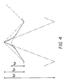
- a preferred embodiment of this waveform is shown in Figure 3 and Figure 4.
- a modified triangle waveform with narrowed peaks is used.
- a method of producing the modified triangle waveform that has an increasing rate of rise to the waveform toward the waveform peak, and a decreasing rate of fall to the waveform leaving the waveform peak is to create an alternating charge and discharge current and integrating to produce a modified triangle waveform.
- Another method would be to combine linear and exponential waveforms. The critical requirement is that the waveform produce narrowed control signals at higher input voltages, reducing the responsiveness of the regulator at higher input voltages.
- Pulse width modulation incorporating this invention is achieved by generating the modifed oscillator signal, comparing the modified oscillator signal to an error signal, and switching a comparator to generate a control signal when the modified oscillator signal exceeds the error signal.
- Voltage regulation with improved stability incorporating this invention is achieved by establishing a feedback control loop from the regulator output to the input of an error amp, comparing the error signal with a modified oscillator signal incorporating this invention to produce a control signal of varying pulse width corresponding to the level of the error signal, and switching the output stage with this control signal.
- the stability of a switching voltage regulator is improved by control of the loop gain by the shape of the waveform of the oscillator signal.
- An improved oscillator waveform automatically functions to suppress the increase in loop gain due to increases in the input voltage increases, thus improving stability over a wider range of input voltages.
- a modified triangle waveform with narrowed peaks is used as the oscillator signal in a pulse width modulator or switching voltage regulator.
- Figure 3 shows the signals at the comparator including the modified oscillator signal in accordance with this invention.
- Figure 3 shows the input signals V error and V osc , and the output signal V control .
- the oscillator signal V osc incorporates this invention, and Figure 3 shows the resultant narrowing of the control signal V control pulses.
- a conventional system would use a linear triangle wave as the oscillator signal V osc as is shown in Figure 2.
- the oscillator signal V osc triangle wave is modified to have a narrowed peak.
- the effect of comparing this modified oscillator signal V osc to the error voltage V error is to produce narrower control signal V control pulses as compared to the conventional system. This has the effect of lowering overall loop gain.
- the modified oscillator waveform has a variable effective peak to peak voltage at various points on the modified oscillator waveform, according to the point at which the error voltage V error intersects the oscillator waveform V osc . If the intersect point is low, the effective peak to peak voltage of the modified oscillator waveform V osc is low like V p3 . A conventional linear triangle wave would have had a somewhat larger effective peak to peak voltage like V p1 . If the intersect point is high, the effective peak to peak voltage of the modified oscillator waveform V osc is large like V p2 . This large effective peak to peak voltage gives reduced loop gain A loop at that point on the modified oscillator waveform V osc . Therefore the loop gain varies and its increase is suppressed at the high effective peak to peak voltage point.
- Figures 5 and 6 show how this modified oscillator waveform functions at low and high input voltages.
- Figure 5 shows the operation at a low input voltage. The input voltage is switched on during the long periods in which the oscillator waveform exceeds the error signal to produce the resultant smoothed average output voltage. At this operating point the comparator is operating on an essentially linear lower portion of the oscillator waveform.
- Figure 6 shows the operation at a high input voltage. To produce the same resultant smoothed average output voltage, the input voltage will be switched for short periods when the oscillator waveform peaks exceed the higher error signal.
- Figure 7 shows a block diagram of an oscillator circuit for producing the modified oscillator signal of this invention.
- the oscillator includes a first source of current 50 of magnitude +I, and a second source of current 52 of opposite direction -I.
- the current sources are alternately selected as a charge or discharge current by a switch 53 to appear on node 54.
- the switch is controlled by a direction control which switches at the frequency of operation selected for the oscillator.
- the current appearing at node 54 is applied to the first plate of an integration capacitor 55 and to a first input 56 of an inverting integration op amp 58.
- the second input 60 of the inverting integration op amp 58 is connected to ground or a low reference voltage.
- the output 62 of the inverting integration op amp 58 provides the oscillator signal V osc and is connected to an oscillator output point 64 and to the second plate of the integration capacitor 55.
- a return connection 66 returns a return signal I ret to the first current source 50 and second current source 52.
- the return signal I ret is developed as a fractional portion of the oscillator signal V osc .
- the return signal I ret carried by the return connection 66 is added as a supplemental current source 67 to the first source of current 50, and added in an opposite direction as a supplemental current source 68 to the second source of current 52. Therefore, the current appearing at node 54 will alternate between +I + I ret and -I -I ret .
- the integration of the -I current generates the rising portion of a triangle waveform.
- the integration of the +I current generates the falling portion of a triangle waveform.
- the integration of the -I ret current adds the increased peak to the rising portion of the oscillator waveform V osc .
- the integration of the +I ret generates the decreasing fall from the peak of the oscillator waveform V osc .
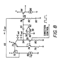
- FIG 8 shows a detailed schematic of an oscillator circuit for producing the modified oscillator signal of this invention. Where possible, similar components are given similar numbers as in Figure 7.
- the oscillator has a first source of current 50 of magnitude +I. This current is established from a supply voltage through a transistor 70 and current sink to a low potential. This current is mirrored from transistor 70 to transistor 72, and is multiplied by a factor of two by making transistor 72 of twice the size of transistor 70. This multiplied current constitutes a second source of current flowing from a supply voltage through transistors 72 and 74 and resistor 76.
- a switch controlled by a pulse train from a direction control is formed by transistor 78 and resistor 80, and the switch controls the application of the first or second sources of current to node 54.
- the integration capacitor 55 and inverting integration op amp 58 are as previously described in Figure 7.
- a return connection 66 from a transistor 79 to the first source of current 50.
- the return signal I ret is developed from the oscillator output 64 by transistor 79, and resistor 82 and voltage reference 80.
- the return signal I ret supplements the first source of current 50. This supplemented current is mirrored by the connection between the bases of transistors 70 and 72, and the current is multiplied by a factor of two by making transistor 72 of twice the size of transistor 70. This multiplied and supplemental current will appear in the second source of current established by transistors 72 and 74 and resistor 76. Therefore, the current at node 54 alternates between +I +I ret and -I -I ret .
- a buffer amplifier stage composed of a transistor 84 and biasing current source 86 is connected to oscillator output 64 to drive the following stages using the modified oscillator signal.
- This circuit will generate the modifed triangle waveform with narrowed peaks shown as V osc in Figure 3 and Figure 4.
- This waveform will provide the advantages of narrowed control signal V control pulses as previously described.
- This oscillator can be incorporated in a voltage regulator as previously described in Figure 1 to obtain a voltage regulator with the advantages of improved loop gain stability.
- the incorporation of this invention can reduce the increase in loop gain by one-half as the input voltage increases from 5 to 30 volts.
- a voltage regulator using a sawtooth waveform as the oscillator waveform could be improved by using a "peaked” or narrowed sawtooth waveform with an increasing rate of rise during the rising portion of the sawtooth. This would result in narrowed control signal pulses as compared to a conventional straight sawtooth waveform. This narrowing would help suppress increases in loop gain as the input voltage increases, and stabilize the operation of the voltage regulator.
Landscapes
- Engineering & Computer Science (AREA)
- Power Engineering (AREA)
- Dc-Dc Converters (AREA)
Applications Claiming Priority (2)
| Application Number | Priority Date | Filing Date | Title |
|---|---|---|---|
| US240319 | 1988-09-06 | ||
| US07/240,319 US4847549A (en) | 1988-09-06 | 1988-09-06 | Switching voltage regulator with stabilized loop gain |
Publications (3)
| Publication Number | Publication Date |
|---|---|
| EP0358098A2 true EP0358098A2 (fr) | 1990-03-14 |
| EP0358098A3 EP0358098A3 (en) | 1990-11-07 |
| EP0358098B1 EP0358098B1 (fr) | 1994-03-30 |
Family
ID=22906072
Family Applications (1)
| Application Number | Title | Priority Date | Filing Date |
|---|---|---|---|
| EP89115966A Expired - Lifetime EP0358098B1 (fr) | 1988-09-06 | 1989-08-30 | Régulateur à commutation de tension à gain stabilisé |
Country Status (5)
| Country | Link |
|---|---|
| US (1) | US4847549A (fr) |
| EP (1) | EP0358098B1 (fr) |
| JP (1) | JP2841085B2 (fr) |
| CA (1) | CA1300680C (fr) |
| DE (1) | DE68914218T2 (fr) |
Cited By (1)
| Publication number | Priority date | Publication date | Assignee | Title |
|---|---|---|---|---|
| DE19936860A1 (de) * | 1999-08-05 | 2001-02-15 | Vacuumschmelze Gmbh | Verlustarmer Spannungswandler |
Families Citing this family (2)
| Publication number | Priority date | Publication date | Assignee | Title |
|---|---|---|---|---|
| US5502416A (en) * | 1995-03-31 | 1996-03-26 | Sgs-Thomson Microelectronics, Inc. | Adjustable reset threshold for an integrated regulator |
| US8719475B2 (en) * | 2010-07-13 | 2014-05-06 | Broadcom Corporation | Method and system for utilizing low power superspeed inter-chip (LP-SSIC) communications |
Family Cites Families (9)
| Publication number | Priority date | Publication date | Assignee | Title |
|---|---|---|---|---|
| JPS5857071B2 (ja) * | 1978-09-20 | 1983-12-17 | 横河電機株式会社 | Dc/dcコンバ−タの制御方式 |
| JPS5836590B2 (ja) * | 1978-09-20 | 1983-08-10 | 横河電機株式会社 | Dc/dcコンバ−タの制御方式 |
| FI793821A7 (fi) * | 1978-12-13 | 1981-01-01 | Rca Corp | Katkova säädin, jossa on itsenäinen takaisinkytkentätien suodatin. |
| JPS6054215B2 (ja) * | 1978-12-29 | 1985-11-29 | 三菱重工業株式会社 | 板状物体の前揃え装置 |
| DE3066074D1 (en) * | 1979-04-09 | 1984-02-16 | Org Europeene De Rech | Current chopper for regulating the supply of a load |
| JPS56129423A (en) * | 1980-03-14 | 1981-10-09 | Sony Corp | Triangle wave generating circuit |
| US4459539A (en) * | 1982-07-12 | 1984-07-10 | Hewlett-Packard Company | Charge transfer constant volt-second regulator |
| US4546421A (en) * | 1984-03-28 | 1985-10-08 | United Technologies Corporation | Flyback feedforward pulse width modulation regulator |
| JPS6165883U (fr) * | 1984-10-01 | 1986-05-06 |
-
1988
- 1988-09-06 US US07/240,319 patent/US4847549A/en not_active Expired - Lifetime
-
1989
- 1989-08-30 DE DE68914218T patent/DE68914218T2/de not_active Expired - Lifetime
- 1989-08-30 EP EP89115966A patent/EP0358098B1/fr not_active Expired - Lifetime
- 1989-09-05 CA CA000610296A patent/CA1300680C/fr not_active Expired - Fee Related
- 1989-09-06 JP JP1229440A patent/JP2841085B2/ja not_active Expired - Lifetime
Cited By (1)
| Publication number | Priority date | Publication date | Assignee | Title |
|---|---|---|---|---|
| DE19936860A1 (de) * | 1999-08-05 | 2001-02-15 | Vacuumschmelze Gmbh | Verlustarmer Spannungswandler |
Also Published As
| Publication number | Publication date |
|---|---|
| US4847549A (en) | 1989-07-11 |
| CA1300680C (fr) | 1992-05-12 |
| EP0358098A3 (en) | 1990-11-07 |
| JP2841085B2 (ja) | 1998-12-24 |
| DE68914218D1 (de) | 1994-05-05 |
| JPH02111255A (ja) | 1990-04-24 |
| EP0358098B1 (fr) | 1994-03-30 |
| DE68914218T2 (de) | 1994-10-06 |
Similar Documents
| Publication | Publication Date | Title |
|---|---|---|
| US4988942A (en) | Switched resistor regulator control when transfer function includes discontinuity | |
| KR100570721B1 (ko) | 작은부하에서효율을향상시킬수있는스위칭레귤레이터 | |
| EP1969705B1 (fr) | Circuit generateur de compensation de pente d'un regulateur de commutation | |
| US4536700A (en) | Boost feedforward pulse width modulation regulator | |
| US8773084B2 (en) | Buck-boost converter using timers for mode transition control | |
| US7126318B2 (en) | Higher order slope compensation for fixed frequency current mode switching regulators | |
| EP0415244B1 (fr) | Générateur de rampe à compensation adaptatif pour les convertisseurs continu-continu en mode de courant | |
| JP2596314B2 (ja) | スイッチング電源回路 | |
| US7075277B2 (en) | DC-DC converter | |
| US6885177B2 (en) | Switching regulator and slope correcting circuit | |
| US5079453A (en) | Slope compensation circuit for stabilizing current mode converters | |
| US6369558B2 (en) | Switching regulator | |
| KR100581042B1 (ko) | 피 에프 엠 시스템의 스위칭 레귤레이터 제어회로 및 스위칭 레귤레이터 | |
| KR20010022479A (ko) | 벅 부스트 스위칭 조정기 | |
| US4847549A (en) | Switching voltage regulator with stabilized loop gain | |
| KR20010050573A (ko) | 히스테리 스위치-모드 전원의 주파수 제어 | |
| US4789818A (en) | DC voltage converter | |
| US4947102A (en) | Feedback loop gain compensation for a switched resistor regulator | |
| US6445168B2 (en) | Power output circuit having a pulse-width modulation mode and a permanently closed mode | |
| US4644254A (en) | Switch controller having a regulating path and an auxiliary regulating path parallel thereto | |
| JP2871067B2 (ja) | 発振回路 | |
| JP3352050B2 (ja) | スイッチング電源制御回路 | |
| US7518345B2 (en) | Device for converting a continuous supply voltage into a continuous output voltage and corresponding electronic circuit | |
| JPH05211766A (ja) | 高デューティサイクル電流制御型pwmレギュレータの安定性を改善する回路 | |
| KR100216355B1 (ko) | 고정주파수 발진회로 |
Legal Events
| Date | Code | Title | Description |
|---|---|---|---|
| PUAI | Public reference made under article 153(3) epc to a published international application that has entered the european phase |
Free format text: ORIGINAL CODE: 0009012 |
|
| AK | Designated contracting states |
Kind code of ref document: A2 Designated state(s): DE FR GB IT NL |
|
| PUAL | Search report despatched |
Free format text: ORIGINAL CODE: 0009013 |
|
| AK | Designated contracting states |
Kind code of ref document: A3 Designated state(s): DE FR GB IT NL |
|
| 17P | Request for examination filed |
Effective date: 19910313 |
|
| 17Q | First examination report despatched |
Effective date: 19930310 |
|
| GRAA | (expected) grant |
Free format text: ORIGINAL CODE: 0009210 |
|
| AK | Designated contracting states |
Kind code of ref document: B1 Designated state(s): DE FR GB IT NL |
|
| REF | Corresponds to: |
Ref document number: 68914218 Country of ref document: DE Date of ref document: 19940505 |
|
| ET | Fr: translation filed | ||
| ITF | It: translation for a ep patent filed | ||
| PGFP | Annual fee paid to national office [announced via postgrant information from national office to epo] |
Ref country code: FR Payment date: 19940812 Year of fee payment: 6 |
|
| PGFP | Annual fee paid to national office [announced via postgrant information from national office to epo] |
Ref country code: NL Payment date: 19940831 Year of fee payment: 6 |
|
| PLBE | No opposition filed within time limit |
Free format text: ORIGINAL CODE: 0009261 |
|
| STAA | Information on the status of an ep patent application or granted ep patent |
Free format text: STATUS: NO OPPOSITION FILED WITHIN TIME LIMIT |
|
| 26N | No opposition filed | ||
| PG25 | Lapsed in a contracting state [announced via postgrant information from national office to epo] |
Ref country code: NL Effective date: 19960301 |
|
| PG25 | Lapsed in a contracting state [announced via postgrant information from national office to epo] |
Ref country code: FR Effective date: 19960430 |
|
| NLV4 | Nl: lapsed or anulled due to non-payment of the annual fee |
Effective date: 19960301 |
|
| REG | Reference to a national code |
Ref country code: FR Ref legal event code: ST |
|
| PGFP | Annual fee paid to national office [announced via postgrant information from national office to epo] |
Ref country code: GB Payment date: 20010803 Year of fee payment: 13 |
|
| REG | Reference to a national code |
Ref country code: GB Ref legal event code: IF02 |
|
| PG25 | Lapsed in a contracting state [announced via postgrant information from national office to epo] |
Ref country code: GB Free format text: LAPSE BECAUSE OF NON-PAYMENT OF DUE FEES Effective date: 20020830 |
|
| GBPC | Gb: european patent ceased through non-payment of renewal fee |
Effective date: 20020830 |
|
| PG25 | Lapsed in a contracting state [announced via postgrant information from national office to epo] |
Ref country code: IT Free format text: LAPSE BECAUSE OF NON-PAYMENT OF DUE FEES;WARNING: LAPSES OF ITALIAN PATENTS WITH EFFECTIVE DATE BEFORE 2007 MAY HAVE OCCURRED AT ANY TIME BEFORE 2007. THE CORRECT EFFECTIVE DATE MAY BE DIFFERENT FROM THE ONE RECORDED. Effective date: 20050830 |
|
| PGFP | Annual fee paid to national office [announced via postgrant information from national office to epo] |
Ref country code: DE Payment date: 20080930 Year of fee payment: 20 |