EP0359238A2 - Gruppenantenne mit IC-Einheiten für die ZF-Umwandlung und für die Verbindung der Antennenelemente mit der Signalverzweigung - Google Patents
Gruppenantenne mit IC-Einheiten für die ZF-Umwandlung und für die Verbindung der Antennenelemente mit der Signalverzweigung Download PDFInfo
- Publication number
- EP0359238A2 EP0359238A2 EP89116962A EP89116962A EP0359238A2 EP 0359238 A2 EP0359238 A2 EP 0359238A2 EP 89116962 A EP89116962 A EP 89116962A EP 89116962 A EP89116962 A EP 89116962A EP 0359238 A2 EP0359238 A2 EP 0359238A2
- Authority
- EP
- European Patent Office
- Prior art keywords
- reference signal
- signal
- antenna device
- antenna
- integrated circuit
- Prior art date
- Legal status (The legal status is an assumption and is not a legal conclusion. Google has not performed a legal analysis and makes no representation as to the accuracy of the status listed.)
- Withdrawn
Links
Images


Classifications
-
- H—ELECTRICITY
- H01—ELECTRIC ELEMENTS
- H01Q—ANTENNAS, i.e. RADIO AERIALS
- H01Q21/00—Antenna arrays or systems
- H01Q21/0006—Particular feeding systems
- H01Q21/0025—Modular arrays
-
- H—ELECTRICITY
- H01—ELECTRIC ELEMENTS
- H01Q—ANTENNAS, i.e. RADIO AERIALS
- H01Q3/00—Arrangements for changing or varying the orientation or the shape of the directional pattern of the waves radiated from an antenna or antenna system
- H01Q3/26—Arrangements for changing or varying the orientation or the shape of the directional pattern of the waves radiated from an antenna or antenna system varying the relative phase or relative amplitude of energisation between two or more active radiating elements; varying the distribution of energy across a radiating aperture
- H01Q3/30—Arrangements for changing or varying the orientation or the shape of the directional pattern of the waves radiated from an antenna or antenna system varying the relative phase or relative amplitude of energisation between two or more active radiating elements; varying the distribution of energy across a radiating aperture varying the relative phase between the radiating elements of an array
- H01Q3/34—Arrangements for changing or varying the orientation or the shape of the directional pattern of the waves radiated from an antenna or antenna system varying the relative phase or relative amplitude of energisation between two or more active radiating elements; varying the distribution of energy across a radiating aperture varying the relative phase between the radiating elements of an array by electrical means
- H01Q3/36—Arrangements for changing or varying the orientation or the shape of the directional pattern of the waves radiated from an antenna or antenna system varying the relative phase or relative amplitude of energisation between two or more active radiating elements; varying the distribution of energy across a radiating aperture varying the relative phase between the radiating elements of an array by electrical means with variable phase-shifters
-
- H—ELECTRICITY
- H05—ELECTRIC TECHNIQUES NOT OTHERWISE PROVIDED FOR
- H05K—PRINTED CIRCUITS; CASINGS OR CONSTRUCTIONAL DETAILS OF ELECTRIC APPARATUS; MANUFACTURE OF ASSEMBLAGES OF ELECTRICAL COMPONENTS
- H05K1/00—Printed circuits
- H05K1/02—Details
- H05K1/0213—Electrical arrangements not otherwise provided for
- H05K1/0237—High frequency adaptations
-
- H—ELECTRICITY
- H05—ELECTRIC TECHNIQUES NOT OTHERWISE PROVIDED FOR
- H05K—PRINTED CIRCUITS; CASINGS OR CONSTRUCTIONAL DETAILS OF ELECTRIC APPARATUS; MANUFACTURE OF ASSEMBLAGES OF ELECTRICAL COMPONENTS
- H05K1/00—Printed circuits
- H05K1/18—Printed circuits structurally associated with non-printed electric components
- H05K1/181—Printed circuits structurally associated with non-printed electric components associated with surface mounted components
Definitions
- the present invention relates to an antenna device for use in reception or transmission of a microwave signal and, in particular, to an array antenna device which is useful for receiving broadcast through a satellite repeater.
- a plurality of antenna elements are arranged in a plane to form an antenna array.
- those antenna elements receive a microwave signal, they produce received signals which are combined by a signal combining circuit to produce a combined signal.
- the combined signal is amplified at an amplifier to produce an amplified signal.
- the amplified signal is frequency-converted into an intermediate-frequency (IF) signal by an IF converting circuit which comprises a mixer, a local oscillator, and an IF amplifier.
- IF intermediate-frequency
- the array antenna device has a degraded noise figure due to use of the signal combining circuit. This is because the signal combining circuit causes a combining loss. Moreover, the signal combining circuit makes a long coupling line between each of the antenna elements and the amplifier and therefore causes a transmission loss.
- MICUs microwave integrated circuit units
- Each of the MICUs comprises one of the antenna elements and an amplifier coupled thereto and is coupled to the signal combining circuit. Therefore, the received signals from the antenna elements are amplified at individual amplifiers to produce amplified signals which are combined by the signal combining circuit to produce a combined signal. The combined signal is applied to the IF conversion circuit.
- each of antenna elements and each of the amplifiers are disposed adjacent to each other. Therefore, a length of the coupling line between the antenna element and the amplifier is considerably reduced so that the transmission loss is reduced between the antenna element and the amplifier.
- the signal combining circuit is also used between the amplifiers and the IF conversion circuit and makes the transmission loss and the combining loss.
- a direction of a main lobe of an array antenna can be changed by use of variable phase shifters in a coupling line for the antenna array.
- the phase shifter causes a large transmission loss, it cannot be used in those array antenna devices shown in Fig. 1 and it is difficult to use the phase shifter in those any antenna devices shown in Fig. 3. Accordingly, it is necessary to move the array antenna device so as to direct the main lobe to the satellite repeater.
- variable phase shifters can be used for adjusting the direction of the main lobe of the array antenna.
- an array antenna device with a plurality of antenna elements comprises a plurality of integrated circuit units each of which comprises: at least one of the antenna elements for receiving a radio wave to deliver a receive signal; amplifier means coupled to the antenna element for amplifying the receive signal as an amplified signal; local oscillator means for oscillating a local signal of a predetermined frequency in synchronism with a reference signal; mixer means coupled to the amplifier means and the local oscillator means for mixing the amplified signal and the local signal to produce an intermediate frequency signal; and an output terminal coupled to the mixer means for delivering the intermediate frequency signal as an output signal.
- the antenna device further comprises combining means coupled to the output terminal of each of the integrated circuit units for combining the output signal from each of the integrated circuit units to produce a combined signal; an output port coupled to the combining means for delivering the combined signal; reference signal generating means for generating the reference signal; and coupling means for coupling the local oscillating means and the reference signal generating means for supplying the reference signal to the local oscillator means.
- each of the integrated circuit units further comprises an intermediate frequency amplifier means connecting the mixer means and the output terminal for amplifying the intermediate frequency signal to deliver the intermediate frequency signal as amplified to the output terminal.
- the antenna device further comprises a plurality of variable phase shifters each coupled between the output terminal and the combining means for shifting a phase of the output signal passing therethrough.
- the reference signal generating means is connected to the conductive line whereby the combining means serves as the coupling means.
- the coupling means comprises signal distributing means connecting the reference signal generating means and each of the integrated circuit units at the input terminal.
- the antenna device further comprises a case, a circuit board mounted in the case and having the plurality of integrated circuit units mounted thereon, the circuit board further having the combining means, the output port, the reference signal generating means, and coupling means formed thereon, and an electric connector mounted on the case and connected to the output port.
- each of the integrated circuit units comprises a reference signal receiving antenna, the reference signal generating means having a reference signal transmitting antenna so that the coupling means is consisted by antenna coupling between the reference signal receiving antenna and the reference signal transmitting antenna.
- each of the antenna element is formed in an integrated circuit unit together with a distributing means for distributing a signal to be transmitted, an integrated circuit chip comprising a frequency conversion circuit means for frequency-converting the signal to produce a converted signal and a power amplifier for amplifying the converted signal to excite the antenna element, and a reference signal generating means for synchronizing the frequency conversion circuit means with one another.
- a known array antenna device shown therein comprises a plurality of antenna elements 311 through 31n (n being natural number) for receiving a radio wave of, for example, 40 GHz band to produce receive signals, a signal combining circuit 32 coupled to the plurality of antenna elements for combining the receive signals to produce a combined signal, and an amplifier 33 coupled to the signal combining circuit for amplifying the combined signal to produce an amplified signal.
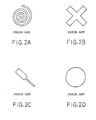
- Each of the antenna elements 311 through 31n is one of a spiral type shown in Fig. 2A, a cross dipole type shown in Fig. 2B, a 1/4 wavelength open-ended line type shown in Fig. 2C, and a batch type shown in Fig. 2D.
- the used type is determined by, for example, polarization of the radio wave.
- the antenna elements 311 through 31n, the signal combining circuit 32 and the amplifier 33 are formed and mounted on a circuit substrate (not shown) which is connected to a mixer 34 by an electric connector (not shown).
- the amplified signal is mixed at the mixer 34 with a local signal from a local oscillator 35 to produce an intermediate frequency (IF) signal of, for example, 1 GHZ.
- IF intermediate frequency
- the IF signal is amplified at an IF amplifier 36.
- FIG. 3 another known array antenna device shown therein is similar to the device of Fig. 1 except that a plurality of amplifiers 331 through 33n are coupled with the plurality of antenna elements 311 through 31n to form a plurality of microwave integrated circuit units (MICUs) 371 through 37n, respectively, which are coupled with the signal combining circuit 32.
- MICUs microwave integrated circuit units
- the receive signals from the antenna elements 311 through 31n are amplified at individual amplifiers 331 through 33n to produce a plurality of amplified signals which are combined at the signal combining circuit 32 to produce a combined signal.
- the combined signal is applied to the mixer 34 and frequency converted into the IF signal.
- the signal combining circuit 32 causes the combining loss and the transmission loss. Therefore, those known array antenna devices have the problems as described in the preamble.
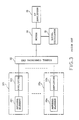
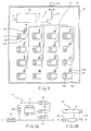
- the array antenna device comprises a plurality of MICUs 381 through 38n wherein the plurality of amplifiers 331 through 33n, a plurality of mixers 341 through 34n and a plurality of local oscillators 351 through 35n are formed together with the plurality of antenna elements 311 through 31n, respectively, by the way of the integrated circuit technique.
- These MICUs 381 through 38n have output terminals 391 through 39n which are coupled with the signal combining circuit 32.
- the signal combining circuit 32 is connected to an output port 40.
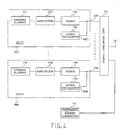
- each of the MICUs is shown at 38 and comprises a case 43 in which a substrate 44 and an IC chip 45 are encapsulated.
- the substrate 44 is made of, for example, alumina ceramic and has the antenna element 31 formed thereon in one of types shown in Figs. 2A-2D by a thin-film circuit forming technique.
- the IC chip 45 has the amplifier 33, the mixer 34 and the local oscillator 42 formed therein. Bonding wires 46 and 47 connect the antenna element 31, the IC chip 45 and terminal plates 48 which are fixedly mounted in the case 43 and extended outside the case 43.
- the case 43 has a radio wave transmission window 49 which is formed of, for example, glass, ceramics, plastics, or the like at a position facing the antenna element 31.
- the case 43 has an inner surface which is partially coated with a metallic film 50 formed by metallizing technique except the window 49.
- the metallic film 50 is for protection of the IC chip 45 against the electromagnetic interference and the ultraviolet ray. It is of course that the metallic film 50 is formed to be insulated from the terminal plates 48. One of the terminal plates is corresponding to the output terminal 39.
- the amplifier 33, mixer 34 and the local oscillator 35 can also be formed in the substrate 29 without use of the IC chip 45 different from the substrate 29.
- the bonding wire 46 can be omitted.
- the amplifier 33 is disposed adjacent the antenna element 31 and the IF conversion circuit comprising the mixer 34 and the local oscillator 42. Therefore, lengths of lines for coupling therebetween are small so that transmission loss is very reduced.
- the antenna device further comprises a reference signal generator 41 electrically coupled to the local oscillators 421 through 42n for generating a reference signal to synchronize the local signals from the local oscillators 421 through 42n with each other.
- the electrical coupling is established by the signal combining circuit 32. That is, the reference signal generator 41 is connected with the signal combining circuit 32.
- the local oscillators 351 through 35n have reference signal input terminals 421 through 42n which are connected to the individual output terminals 391 through 39n. Therefore, the reference signal from the reference signal generating circuit 41 is delivered to the local oscillators 351 through 35n through the signal combining circuit 32, the output terminals 391 through 39n and the reference signal input terminals 421 through 42n.
- the circuit board 51 is fixed in a housing 52 which has an electrical connector 53 corresponding to the output port 40.
- the signal combining circuit 32 comprises strip lines extending on the circuit board 51 shown in the figure and connecting the MICUs 381 through 38n to the connector 53 through a chip capacitor C1.
- the reference signal generator 41 is also connected to the MICUs 381 through 38n through the strip lines.
- the reference signal generator 41 is shown by a box of a chain line in the figure for the purpose of simplification of the drawings but is shown in Fig. 6A in detail.
- the reference signal generator 41 comprises a transistor T, a chip capacitor C2, and four (4) chip resistors R1 through R4 shown therein.
- the terminals A and B are connected to A and B in Fig. 6.
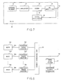
- another MICU 54 shown therein comprises the antenna element 31, the amplifier 33, the mixer 34 and the local oscillator 35 similar to the MICU 38 in Fig. 4 but further comprises the IF amplifier 36.
- the IF amplifier 36 is connected to an output terminal 55 of the MICU and the reference signal terminal 42 of the local oscillator 35 is also connected to the output terminal 55.
- the IF signal from the mixer 34 is amplified at the IF amplifier 36 and is provided to the output terminal 55 as an amplified IF signal.
- the MICU 54 is also realized to have a structure similar to that of Figs. 5A and 5B.
- the IC chip comprises not only the amplifier, the mixer and the local oscillator but also the IF amplifier.
- the MICU 54 can be substituted for each of MICUs 381 through 38n in Fig. 4.
- the shown array antenna device is similar to that of Fig. 4 but uses a plurality of MICUs of Fig. 7 as shown at 541 through 54n in place of MICUs 381 through 38n, a plurality of variable phase shifters 561 through 56n connected to the MICUs and a band stop filter 57.
- a direction of the main lobe of the array antenna is adjusted by adjusting the variable phase shifters 561 through 56n.
- the band stop filter 57 is for preventing the combined signal from applying to the reference signal generator 41.
- MICUs 541 through 54n can be replaced by MICUs 381 through 38n in Fig. 4.
- the array antenna device of Fig. 8 can be realized with a structure as shown in Figs. 9, 9A and 9B.
- the shown structure is similar to that in Fig. 6 except that the band stop filter 57 and variable phase shifters 561 through 56n are used and that the MICU of Fig. 7 is used in place of each of the MICUs in Fig. 6.
- Fig. 9 the reference signal generator 41 and band stop filter 57 are shown by boxes of chain lines. But, they are shown in Figs. 9A and 9B in detail, respectively.
- the reference signal generator 41 in Fig. 9A is equivalent of that in Fig. 6A but is only different in disposition of the circuit elements T, C2, and R1 through R4.
- the band stop filter 57 comprises a ground potential strip line G, two capacitors C3 and C4, and an inductor L.
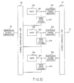
- the array antenna device according to the third embodiment shown therein is a modification of the array antenna device of Fig. 8.
- the reference signal generator 41 is coupled to the output terminals 551 through 55n of the MICUs 541 through 54n through not the signal combining circuit 32 but a signal distributing circuit 58 and band stop filters 571 through 57n. Therefore, the reference signal from the reference signal generator 41 is applied to the local oscillators (35 in Fig. 7) in the MICUs 541 trough 54n through the signal distributing circuit 58 and band stop filters 571 through 57n.
- the array antenna device of Fig. 10 is realized similar to that shown in Figs. 9, 9A and 9B.
- the signal combining circuit 32 and the variable phase shifters 561 through 56n are formed similar to those in Fig. 9.
- the signal distributing circuit 58 comprises micro strip lines and connects the reference signal generator 41 and the MICUs 541 through 54n through band stop filters 571 through 57n.
- the band stop filters 571 through 57n are shown by boxes of chain lines but can have a circuit structure similar to that shown in Fig. 9B.
- the reference signal generator 41 is also shown by a box of a chain line but has a circuit structure sown in Fig. 11A.
- the circuit of Fig. 11A is equivalent to that of Fig. 9A but is only different from it in disposition of the circuit elements T, C2, and R1 through R4.
- the array antenna device according to the fourth embodiment shown therein is a modification of the array antenna device of Fig. 10. That is, the variable phase shifters 561 through 56n are disposed to connect the signal distributing circuit 58 and the band stop filters 561 through 56n. It will be understood that the array antenna device is also realized similar to that of Fig. 11 with the difference of disposition of the variable phase shifters 561 through 56n.
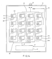
- the array antenna device according to the fifth embodiment shown therein is a modification of the device of Fig. 4.
- Each of MICUs used therein is only different from each of MICUs 381 through 38n in Fig. 4 in that it has an input terminal connected to the reference signal input terminal 42 of the local oscillator 35.
- the reference signal input terminal 42 is not connected to the output terminal 39. Therefore, the MICUs in this embodiment are represented by the same reference numeral with a prime (′), that is, 38′1 through 38′n.
- the input terminals are represented by 591 through 59n.
- each of MICUs 38′1 through 38′n can be formed with a structure similar to that of Figs. 5A and 5B.
- Another of the terminal plates 48 is connected to the local oscillator in the IC chip 45 and is corresponding to the input terminal 59.
- the reference signal generator 41 is connected to the input terminals 591 through 59n of MICUs 38′1 through 38′n.
- the array antenna device can be realized on a circuit board similar to Fig. 6.
- the MICUs 38′1 through 38′n and the signal combining circuit 32 are formed on the circuit board 51 similar to that of Fig. 6.
- the signal distributing circuit 38 is formed on the circuit board 51 to connect the reference signal generator 41 and terminal plates corresponding to the input terminals 591 through 59n of MICUs 38′1 through 38′n.
- the reference signal generator 41 is formed similar to that of Fig. 11A. It should be appreciated that the terminals A and B in Fig. 11A are connected to terminals A and B in Fig. 14.
- the array antenna device according to the fifth embodiment is a modification of the array antenna device of Fig. 13 by use of variable phase shifters 561 through 56n in the lines connecting the output terminals 391 through 39n and the signal distributing circuit 32.
- a direction of the main lobe of the antenna array can be adjusted by adjusting the variable phase shifters 561 through 56n.
- the array antenna device can be realized on the circuit board 51 in Fig. 14 by disposing the variable phase shifters 561 through 56n at positions similar to those in Fig. 9.
- the shown array antenna device according to the seventh embodiment is a modification of Fig. 15 by displacing the variable phase shifters 561 through 56n in the lines connecting the signal distributing circuit 58 and the input terminals 591 through 59n of the MICUs 38′1 through 38′n.
- the array antenna device is also realized on the circuit board 51 in Fig. 14 by disposing the variable phase shifters 561 through 56n in the lines connecting the signal distributing circuit 58 and the input terminals 591 through 59n of the MICUs 38′1 through 38′n.
- FIG. 17 another MICU shown therein is similar to the MICU 54 of Fig. 7 but has an input terminal connected to the reference signal input terminal 42 of the local oscillator 35.
- the reference signal input terminal 42 is not connected to the output terminal 55. Therefore, the MICU of the figure is represented by the same numeral 54 with a prime (′) and the input terminal is represented by 60.
- the MICU 54′ is also similar to the MICU in Fig. 13 except the IF amplifier 36.
- MICU 54′ can be used in place of MICU 38′ in the devices of Figs. 13, 15 and 16.
- the MICU 54′ is also formed to have a structure similar to that shown in Figs. 5A and 5B by forming the IF amplifier 36 in the IC chip 45 while the local oscillator 35 being connected to another of terminal plates 48 which is corresponding to the input terminal 60.
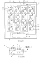
- the eighth embodiment shown therein uses a plurality of MICUs of Fig. 17 which are represented at 54′1 through 54′n.
- the array antenna device of the figure is similar to that of Fig. 8 except that the reference signal is applied to the MICUs through the input terminals 601 through 60n bypassing the variable phase shifters 561 through 56n and the output terminals of the MICUs, respectively.
- the array antenna device can be realized on the circuit board 51 in Fig. 9 by replacing the MICUs 541 through 54n by the MICUs 54′1 through 54′n and by forming additional micro strip lines to connect the micro strip lines of the signal combining circuit 32 to the terminal plates of MICUs 54′1 and 54′n corresponding to the input terminals 601 through 60n.
- the shown ninth embodiment is a modification of the array antenna device of Fig. 18. That is, the output terminals 551 through 55n of MICUs 54′1 through 54′n are directly connected to the signal combining circuit 32 while the input terminals 601 through 60n are connected to the signal combining circuit 32 through the variable phase shifters 561 56n.
- the array antenna device of Fig. 19 can be also formed on the circuit board by modifying formation of Fig. 9.
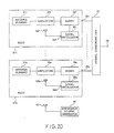
- the tenth embodiment shown therein is characterized in that wireless coupling is made between the local oscillator in the MICU and the reference signal generator by use of antennas, but is similar to the array antenna device of Fig. 4 in the other circuit formation. That is, MICUs 611 through 61n shown in the figure are similar to MICUs 381 through 38n in Fig. 4 except reference signal receiving antennas 621 which are connected to the reference signal input terminals 421 through 42n of the local oscillators 351 through 35n. The reference signal input terminals 421 through 42n are not connected to the output terminals 391 through 39n.
- the reference signal receiving antennas 621 through 62n can be made as strip lines on the IC chips (45 in Fig. 5B).
- the reference signal generator 41 is also provided with a reference signal transmitting antenna 63.
- the reference signal is radiated from the reference signal transmitting antenna 63 and is received at the reference signal receiving antennas 621 through 62n in the MICUs 611 through 61n. Accordingly, the local oscillators 351 through 35n are synchronized with one another.
- each of the MICUs 611 through 61n can be provided with IF amplifiers between the mixer 34 and the output terminal 39 as shown in Fig. 7.
- the array antenna device of Fig. 20 is also formed on the circuit board 51 in the similar way as in Fig. 6.
- the MICUs 611 through 61n, the signal combining circuit 32 and the reference signal generator 41 are formed on the circuit board 51.
- the reference signal transmitting antenna 63 is formed as a strip line on the circuit board 51.
- the reference signal generator 41 is shown as a box of a chain line but has the circuit structure of Fig. 11A. Terminals A and B in Fig. 11A should be connected to terminals A and B in Fig. 21.
- the eleventh embodiment shown therein is a modification of the embodiment of Fig. 20 by using MICUs 38′1 through 38′n of Fig. 13 and by forming the reference signal receiving antennas outside the MICUs as shown at 641 through 64n.
- the array antenna device of Fig. 22 can be realized as shown in Fig. 23 with an arrangement similar to that shown in Fig. 21.
- the MICUs 38′1 through 38′n are used in place of the MICUs 611 through 61n.
- the reference signal antennas 641 through 64n are formed as micro strip lines on the circuit board and are connected to terminal plates of MICUs corresponding to the reference signal input terminals 591 through 59n.
- the reference signal generator 41 shown by a box of a chain line has the circuit structure shown in Fig. 11A.
- the terminals A and B in Fig. 11A should be connected to terminals A and B in Fig. 23.
- the shown twelfth embodiment is a modification of the embodiment of Fig. 22 by using variable phase shifters 561 through 56n in the lines connecting the output terminals 391 through 39n of the MICUs 38′1 through 38′n and the signal combining circuit 32.
- the array antenna device of Fig. 24 can also be realized in a structure similar to that of Fig. 23 but the variable phase shifters 561 through 56n are provided on the circuit board 51 as shown in Fig. 9.
- the MICU 54′ of Fig. 17 can be used in place of each of the MICUs 38′1 through 38′n.
- a radiating antenna device is realized by replacing the amplifier 331, the output terminal 39 and 55, the signal combining circuit 32, and output port 40 by a power amplifier, an input terminal, a signal distributing circuit and an input port, respectively.
- a resultant device for example, in Fig. 4, an IF signal to be transmitted is applied to the input port (40) and is distributed to each of MICUs 381 through 38n.
- the signal is mixed at the mixer (34) with the local signal from the local oscillator (42) to produce a frequency converted signal.
- the frequency converted signal is power-amplified at the power amplifier (33) to produce a transmission signal which is applied to the antenna element (31).
- the transmission signal is radiated from the antenna element as a radio wave.
- a direction of the main lobe of the antenna array is also adjusted by use of variable phase shifters as shown in, for example, Fig. 8.
Landscapes
- Variable-Direction Aerials And Aerial Arrays (AREA)
Applications Claiming Priority (4)
| Application Number | Priority Date | Filing Date | Title |
|---|---|---|---|
| JP230382/88 | 1988-09-13 | ||
| JP23038288A JPH0278301A (ja) | 1988-09-13 | 1988-09-13 | アンテナ装置 |
| JP24722588A JPH0295002A (ja) | 1988-09-30 | 1988-09-30 | アンテナ装置 |
| JP247225/88 | 1988-09-30 |
Publications (2)
| Publication Number | Publication Date |
|---|---|
| EP0359238A2 true EP0359238A2 (de) | 1990-03-21 |
| EP0359238A3 EP0359238A3 (de) | 1991-05-22 |
Family
ID=26529311
Family Applications (1)
| Application Number | Title | Priority Date | Filing Date |
|---|---|---|---|
| EP19890116962 Withdrawn EP0359238A3 (de) | 1988-09-13 | 1989-09-13 | Gruppenantenne mit IC-Einheiten für die ZF-Umwandlung und für die Verbindung der Antennenelemente mit der Signalverzweigung |
Country Status (2)
| Country | Link |
|---|---|
| EP (1) | EP0359238A3 (de) |
| AU (1) | AU633270B2 (de) |
Cited By (7)
| Publication number | Priority date | Publication date | Assignee | Title |
|---|---|---|---|---|
| EP0588179A1 (de) * | 1992-09-10 | 1994-03-23 | Daimler-Benz Aerospace Aktiengesellschaft | Schaltungsanordnung zum Betreiben einer breitbandigen phasengesteuerten Gruppenantenne |
| US5678219A (en) * | 1991-03-29 | 1997-10-14 | E-Systems, Inc. | Integrated electronic warfare antenna receiver |
| WO1998021833A1 (en) * | 1996-11-14 | 1998-05-22 | Nokia Telecommunications Oy | Transmitter unit and base station |
| EP1233527A1 (de) * | 2001-02-17 | 2002-08-21 | Astrium Gmbh | Sende/Empfangssystem einer aktiven Antenne |
| US20120319746A1 (en) * | 2010-03-04 | 2012-12-20 | Mitsubishi Electric Corporation | Array antenna apparatus |
| US10044329B2 (en) | 2015-07-14 | 2018-08-07 | Mitsubishi Electric Corporation | Transmission module, array antenna device including transmission module, and transmission device including transmission module |
| CN109587706A (zh) * | 2017-09-28 | 2019-04-05 | 中国移动通信集团浙江有限公司 | 一种小区覆盖方向自适应调整方法和装置 |
Family Cites Families (6)
| Publication number | Priority date | Publication date | Assignee | Title |
|---|---|---|---|---|
| NL7807170A (nl) * | 1978-06-30 | 1980-01-03 | Hollandse Signaalapparaten Bv | Radarsysteem. |
| US4321605A (en) * | 1980-01-29 | 1982-03-23 | Hazeltine Corporation | Array antenna system |
| USRE32369E (en) * | 1980-11-17 | 1987-03-10 | Ball Corporation | Monolithic microwave integrated circuit with integral array antenna |
| CA1238713A (en) * | 1984-06-04 | 1988-06-28 | Alliedsignal Inc. | Antenna feed network |
| AU4821085A (en) * | 1985-10-02 | 1987-04-09 | Allied Corporation | Antenna feed network |
| US4724441A (en) * | 1986-05-23 | 1988-02-09 | Ball Corporation | Transmit/receive module for phased array antenna system |
-
1989
- 1989-09-13 EP EP19890116962 patent/EP0359238A3/de not_active Withdrawn
- 1989-09-13 AU AU41421/89A patent/AU633270B2/en not_active Ceased
Cited By (13)
| Publication number | Priority date | Publication date | Assignee | Title |
|---|---|---|---|---|
| US5678219A (en) * | 1991-03-29 | 1997-10-14 | E-Systems, Inc. | Integrated electronic warfare antenna receiver |
| EP0588179A1 (de) * | 1992-09-10 | 1994-03-23 | Daimler-Benz Aerospace Aktiengesellschaft | Schaltungsanordnung zum Betreiben einer breitbandigen phasengesteuerten Gruppenantenne |
| WO1998021833A1 (en) * | 1996-11-14 | 1998-05-22 | Nokia Telecommunications Oy | Transmitter unit and base station |
| AU726323B2 (en) * | 1996-11-14 | 2000-11-02 | Nokia Telecommunications Oy | Transmitter unit and base station |
| EP1233527A1 (de) * | 2001-02-17 | 2002-08-21 | Astrium Gmbh | Sende/Empfangssystem einer aktiven Antenne |
| EP2544301A4 (de) * | 2010-03-04 | 2014-05-07 | Mitsubishi Electric Corp | Gruppenantennenvorrichtung |
| US20120319746A1 (en) * | 2010-03-04 | 2012-12-20 | Mitsubishi Electric Corporation | Array antenna apparatus |
| US8914068B2 (en) | 2010-03-04 | 2014-12-16 | Mitsubishi Electric Corporation | Array antenna apparatus |
| US10044329B2 (en) | 2015-07-14 | 2018-08-07 | Mitsubishi Electric Corporation | Transmission module, array antenna device including transmission module, and transmission device including transmission module |
| EP3324202A4 (de) * | 2015-07-14 | 2019-02-20 | Mitsubishi Electric Corporation | Übertragungsmodul, gruppenantennenvorrichtung damit und übertragungsvorrichtung |
| EP3324202B1 (de) * | 2015-07-14 | 2026-04-22 | Mitsubishi Electric Corporation | Übertragungsmodul, gruppenantennenvorrichtung damit und übertragungsvorrichtung |
| CN109587706A (zh) * | 2017-09-28 | 2019-04-05 | 中国移动通信集团浙江有限公司 | 一种小区覆盖方向自适应调整方法和装置 |
| CN109587706B (zh) * | 2017-09-28 | 2022-04-15 | 中国移动通信集团浙江有限公司 | 一种小区覆盖方向自适应调整方法和装置 |
Also Published As
| Publication number | Publication date |
|---|---|
| AU4142189A (en) | 1990-03-22 |
| EP0359238A3 (de) | 1991-05-22 |
| AU633270B2 (en) | 1993-01-28 |
Similar Documents
| Publication | Publication Date | Title |
|---|---|---|
| US6556169B1 (en) | High frequency circuit integrated-type antenna component | |
| US6909401B2 (en) | Antenna device | |
| US11936096B2 (en) | Wiring substrate, antenna module, and communication device | |
| JP3275632B2 (ja) | 無線通信装置 | |
| US7102896B2 (en) | Electronic component module | |
| CN113632224B (zh) | 威尔金森分配器 | |
| US6339408B1 (en) | Antenna device comprising feeding means and a hand-held radio communication device for such antenna device | |
| US6628230B2 (en) | Radio frequency module, communication device, and radar device | |
| US7130590B2 (en) | Transceiver assembly | |
| US12126070B2 (en) | Antenna module and communication device equipped with the same | |
| US20060033663A1 (en) | Combined optical and electromagnetic communication system and method | |
| GB2423642A (en) | Flexible compact antenna module mounting arrangement | |
| WO2011078029A1 (ja) | アンテナ素子への配線距離を最短にするアレイアンテナ装置 | |
| CN112400255B (zh) | 天线模块和搭载有该天线模块的通信装置 | |
| US20220085521A1 (en) | Antenna module and communication device equipped with the same | |
| CN112189280A (zh) | 天线模块和通信装置 | |
| JP2002198852A (ja) | アンテナ一体化ミリ波回路 | |
| EP0359238A2 (de) | Gruppenantenne mit IC-Einheiten für die ZF-Umwandlung und für die Verbindung der Antennenelemente mit der Signalverzweigung | |
| CN111262003A (zh) | 天线封装模组和电子设备 | |
| US20060160500A1 (en) | VSAT block up converter (BUC) chip | |
| US20020102959A1 (en) | High power block upconverter | |
| US6914787B2 (en) | Electronic component module | |
| JP4309529B2 (ja) | アンテナ一体型分波器基板 | |
| JP3076000B2 (ja) | アンテナ装置 | |
| JP2002084110A (ja) | 電力合成分配器 |
Legal Events
| Date | Code | Title | Description |
|---|---|---|---|
| PUAI | Public reference made under article 153(3) epc to a published international application that has entered the european phase |
Free format text: ORIGINAL CODE: 0009012 |
|
| 17P | Request for examination filed |
Effective date: 19891006 |
|
| AK | Designated contracting states |
Kind code of ref document: A2 Designated state(s): DE FR GB IT NL SE |
|
| PUAL | Search report despatched |
Free format text: ORIGINAL CODE: 0009013 |
|
| RHK1 | Main classification (correction) |
Ipc: H01Q 3/36 |
|
| AK | Designated contracting states |
Kind code of ref document: A3 Designated state(s): DE FR GB IT NL SE |
|
| 17Q | First examination report despatched |
Effective date: 19920706 |
|
| STAA | Information on the status of an ep patent application or granted ep patent |
Free format text: STATUS: THE APPLICATION IS DEEMED TO BE WITHDRAWN |
|
| 18D | Application deemed to be withdrawn |
Effective date: 19930119 |