EP0359416A2 - Hybridschaltungen - Google Patents
Hybridschaltungen Download PDFInfo
- Publication number
- EP0359416A2 EP0359416A2 EP89308460A EP89308460A EP0359416A2 EP 0359416 A2 EP0359416 A2 EP 0359416A2 EP 89308460 A EP89308460 A EP 89308460A EP 89308460 A EP89308460 A EP 89308460A EP 0359416 A2 EP0359416 A2 EP 0359416A2
- Authority
- EP
- European Patent Office
- Prior art keywords
- recess
- insert
- layers
- pressure pad
- stack
- Prior art date
- Legal status (The legal status is an assumption and is not a legal conclusion. Google has not performed a legal analysis and makes no representation as to the accuracy of the status listed.)
- Withdrawn
Links
Images


Classifications
-
- H—ELECTRICITY
- H10—SEMICONDUCTOR DEVICES; ELECTRIC SOLID-STATE DEVICES NOT OTHERWISE PROVIDED FOR
- H10W—GENERIC PACKAGES, INTERCONNECTIONS, CONNECTORS OR OTHER CONSTRUCTIONAL DETAILS OF DEVICES COVERED BY CLASS H10
- H10W70/00—Package substrates; Interposers; Redistribution layers [RDL]
- H10W70/01—Manufacture or treatment
- H10W70/05—Manufacture or treatment of insulating or insulated package substrates, or of interposers, or of redistribution layers
-
- H—ELECTRICITY
- H10—SEMICONDUCTOR DEVICES; ELECTRIC SOLID-STATE DEVICES NOT OTHERWISE PROVIDED FOR
- H10W—GENERIC PACKAGES, INTERCONNECTIONS, CONNECTORS OR OTHER CONSTRUCTIONAL DETAILS OF DEVICES COVERED BY CLASS H10
- H10W90/00—Package configurations
Definitions
- This invention relates to hybrid circuits and in particular to co-fired hybrid circuits, and methods of manufacture thereof.
- a hybrid circuit is a circuit arrangement consisting of a number of insulating layers in a multilayer structure.
- the layers carry conductive circuit patterns and conductive via connections can be provided between different layers through the layers.
- a recess or cavity can be provided in a cofired structure and one or more semiconductor devices can be mounted in the recess and electrically connected by wires to appropriate conductors of the structure, for example, which are exposed at the recess.
- Such cavity/recess structures have been impracticable to produce using conventional thick film techniques in which each additional layer is built up and fired in sequence, in view of the overall depth required for a suitable recess. The necessary sequential processing is very lengthy, as well as costly and yield is poor.
- High temperature co-firing ceramics are available. By co-firing is meant that a multilayer structure is built up and then fired, rather than having to fire each applied layer in sequence. These co-firing ceramics fire at temperatures of the order of 1400°C and require high-temperature-resistant conductor systems such as tungsten, but this is disadvantageous due to its high resistance.
- Low-temperature co-firing ceramics are now available in a flexible tape form, such as that supplied by Dupont under the designation AT 851. These materials fire at 850°C and therefore gold and silver can be used for interconnections and vias. It is possible to use silver, rather than the less mobile gold, since the structure is hermetic.
- a recessed multilayer structure can be readily built up from insulating sheets cut out of such a flexible tape with appropriate apertures in some of the insulating sheets. The sheets are initially cut from the tape form in which the low temperature co-firing ceramic is supplied and provided with registration holes punched in their corners. The conductive patterns and vias are then formed with use of appropriate conductive inks.
- the vias are formed by cutting holes through the sheets where required and filling them with a suitable conductive ink.
- the conductive patterns are formed by appropriate screen printing on the uppermost surface of the sheets requiring them.
- the next stage is to stack the sheets together with the registration holes aligned and bond them together, in a lamination process, into a unitary structure which can be fired subsequently.
- the sheets can be stacked in a die which includes alignment pins corresponding to the registration holes.
- lamination may involve the use of a uniaxial press at a temperature of the order of 70 to 80°C and a pressure of the order of 3000PSI.
- a method of manufacturing a co-fired hybrid circuit having a recess including a laminating step in which a stack of layers, one or more of which is apertured to provide said recess, are pressed together, characterised in that during the laminating step an insert is disposed in the recess and a resilient pressure pad is disposed over an end face of the stack including the recess.
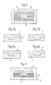
- One basic method which can be employed to produce a structure as indicated in Figure 1 with a recess extending part way thereinto is to produce the structure in various stages.
- a first stage the necessary layers to provide a base 1 are provided with the required conductive patterns and vias and laminated together.
- further layers which will together provide the recess walls are provided with the required conductive patterns and vias, are assembled together, the recess (cavity) is punched out and then the aperture layers are laminated together to form apertured element 2.
- the base 1 and the apertured element 2 are laminated together.
- the basic method was further modified. Different levels of the package were laminated and then the cavity was punched where level thickness permitted. Then the overall package was partially laminated with the cavity walls and base under only low pressure (*1500 PSI) to minimise distortion. The partially laminated package was then used as a mould to cast an integral rubber insert and pressure plate 3 ( Figure 2). This insert and pressure plate 3 is used in conjunction with a laminating jig 4 to laminate a multilayer package 5.
- a resilient (rubber) moulding compound ensures that the laminating pressure is evenly distributed all over the package including in the x, y directions. This results in a package with a flat base to the recess and straight sided recess walls, i.e.
- a punch 6 co-operates with a die 7 to punch an aperture in a green (unfired) ceramic sheet 8.
- the punched aperture side walls of the green (unfired) tape are not perpendicular to the plane of the tape. It is a basic law of press tools that the maximum shear stress is at 45°C to the applied force and this results in the punched holes 8a having side walls at 45 o as shown in Figure 4 for a punching force applied in the direction of arrow 6a ( Figure 3).
- a stack of such punched tapes thus presents a cavity with side walls of an irregular, substantially saw-tooth cross-section in Figure 5.
- the rubber moulding compound used for the insert and pressure plate applies equal pressure in all directions so there is a no tendency to iron out the irregularities in the side walls, although the bowing will be prevented.
- steel inserts 3b ( Figure 6) are disposed in the cavities per se, and possibly on the top surface as shown, in order to ensure that the wall of the stepped cavity are smooth and a rubber moulding pressure pad 3a is disposed over the entire arrangement in the laminating jig in order to ensure that the insert thickness is not critical and leading to an evenly compacted substrate.
- unitary hard tooling providing the combined functions of the steel inserts and the pressure pad over the package is disadvantageous. If unitary hard tooling 9 is dimensioned to suit the prelaminated stack of layers 10 as in Figure 7a, upon lamination ( Figure 7b) the base of the package will be much more compacted than the walls of the cavity because both parts will have been reduced in thickness by the same amount but at the base this reduction in thickness is spread over less sectional thickness. As the base is compacted to a greater extent it will shrink less than the walls of the cavity when fired and thus there will be a tendency for cracks to develop.
- a resilient element in the laminating process either as a pressure pad in conjunction with steel inserts in the recess proper or moulded to shape to fit the recess and provide the pressure pad as well, as described above.
- the recess is multi-stepped.
- the first step is to manufacture a mould for the recess. This comprises a model of the unfired laminated package made up by assembling a set of punched and unpunched sheets of the co-firing ceramic. The required number of sheets 25 are punched with the appropriate cavity apertures.
- the base 26 should be sufficiently thick to provide a flat base to the cavity and may comprise two (as shown) or more sheets. The sheets of the separate levels are laminated together using a watered down (50 - 50) PVA adhesive to glue them together.
- the package is laminated together one level at a time also using the watered down PVA adhesive.
- the lamination is preferably carried out in the laminating jig, between two MYLAR (Registered Trade Mark) sheets, which have been sprayed with a mould release agent, at a pressure of the order of 2 PSI for ten to fifteen minutes.
- the levels are laminated together successively, starting with the base 26, then the base to the first apertured level 27, then the next level is added and so on to produce the mould structure 28 of Figure 11. Following drying the mould is placed in lamination jig 29 ( Figure 12). The inside of the jig and the top surface of the mould are sprayed with a mould release agent.
- a rubber moulding compound is then mixed as appropriate, de-aired by placing in a vacuum chamber and poured into the jig to a suitable height above the mould, typically 1/8" to 1/4" for sheets of the order of 3 inches square.
- the moulding compound is de-aired again and then cured as appropriate.
- red medium viscosity silicone rubber SILASTIC (Registered Trade Mark) 3120 RTV supplied by Dow Corning, curing comprises sixteen hours at room temperature followed by twenty four hours at 70°C. There thus results a rubber mould 33.
- the mould is so produced it may be used for lamination as follows, referring firstly to Figure 13. Place the top plunger 30 of the laminating jig into the square jig frame 31 followed by the bottom plunger 32 i.e. that part with the location/alignment pins. A filter paper may now be placed over the jig bottom plunger 32. The package 34 of low temperature co-firing ceramic sheets is then laid up in the standard manner starting with the base and working upwards. The rubber mould 33 is placed over the laid up ceramic sheets ensuring it is properly located in the cavity. The square jig frame 31 is lifted ( Figure 14) to the level of the bottom plunger 32, and the base plunger and frame slid off the top plunger which is then lowered into the frame ( Figure 15).
- Lamination is carried out at 3500 PSI at 70°C for ten minutes. Following lamination the plungers 30 and 32 are extracted from the frame by moving the plungers upwards and the frame downwards as indicated by the arrows in Figure 14. This ensures that the edges of the package are not bent during extraction from the jig.
Landscapes
- Production Of Multi-Layered Print Wiring Board (AREA)
- Press-Shaping Or Shaping Using Conveyers (AREA)
Applications Claiming Priority (2)
| Application Number | Priority Date | Filing Date | Title |
|---|---|---|---|
| GB8821835 | 1988-09-16 | ||
| GB8821835A GB2222800B (en) | 1988-09-16 | 1988-09-16 | Hybrid circuits |
Publications (2)
| Publication Number | Publication Date |
|---|---|
| EP0359416A2 true EP0359416A2 (de) | 1990-03-21 |
| EP0359416A3 EP0359416A3 (de) | 1991-06-12 |
Family
ID=10643758
Family Applications (1)
| Application Number | Title | Priority Date | Filing Date |
|---|---|---|---|
| EP19890308460 Withdrawn EP0359416A3 (de) | 1988-09-16 | 1989-08-21 | Hybridschaltungen |
Country Status (2)
| Country | Link |
|---|---|
| EP (1) | EP0359416A3 (de) |
| GB (1) | GB2222800B (de) |
Cited By (3)
| Publication number | Priority date | Publication date | Assignee | Title |
|---|---|---|---|---|
| FR2658661A1 (fr) * | 1990-02-20 | 1991-08-23 | Cabot Ceramics Inc | Empilage de modules de circuits integres. |
| EP0695631A1 (de) * | 1994-07-28 | 1996-02-07 | International Business Machines Corporation | Verfahren zum Herstellen keramischer Mehrschichtsubstrate mit zentraler Öffnung |
| KR100473773B1 (ko) * | 2001-03-23 | 2005-03-09 | 가부시키가이샤 무라타 세이사쿠쇼 | 다층 세라믹 기판 제조 방법 |
Families Citing this family (3)
| Publication number | Priority date | Publication date | Assignee | Title |
|---|---|---|---|---|
| JP3225666B2 (ja) * | 1993-01-27 | 2001-11-05 | 株式会社村田製作所 | キャビティ付きセラミック多層ブロックの製造方法 |
| DE4343206A1 (de) * | 1993-12-17 | 1995-06-22 | Bayer Ag | Verfahren zur Herstellung von Rohlingen für Ausweiskarten |
| US5538582A (en) * | 1994-09-14 | 1996-07-23 | International Business Machines Corporation | Method for forming cavities without using an insert |
Family Cites Families (7)
| Publication number | Priority date | Publication date | Assignee | Title |
|---|---|---|---|---|
| US4630172A (en) * | 1983-03-09 | 1986-12-16 | Printed Circuits International | Semiconductor chip carrier package with a heat sink |
| US4643935A (en) * | 1986-01-21 | 1987-02-17 | Burroughs Corporation | Epoxy-glass integrated circuit package having bonding pads in a stepped cavity |
| US4636275A (en) * | 1986-01-21 | 1987-01-13 | Burroughs Corporation | Elastic bladder method of fabricating an integrated circuit package having bonding pads in a stepped cavity |
| US4680075A (en) * | 1986-01-21 | 1987-07-14 | Unisys Corporation | Thermoplastic plug method of fabricating an integrated circuit package having bonding pads in a stepped cavity |
| US4737208A (en) * | 1986-09-29 | 1988-04-12 | American Telephone And Telegraph Company, At&T Bell Laboratories | Method of fabricating multilayer structures with nonplanar surfaces |
| GB2199182A (en) * | 1986-12-18 | 1988-06-29 | Marconi Electronic Devices | Multilayer circuit arrangement |
| ATE87126T1 (de) * | 1987-01-28 | 1993-04-15 | Unisys Corp | Verfahren, das eine elastische folie benutzt zum herstellen einer integrierten schaltungspackung mit kontaktflecken in einer abgestuften grube. |
-
1988
- 1988-09-16 GB GB8821835A patent/GB2222800B/en not_active Expired - Fee Related
-
1989
- 1989-08-21 EP EP19890308460 patent/EP0359416A3/de not_active Withdrawn
Cited By (3)
| Publication number | Priority date | Publication date | Assignee | Title |
|---|---|---|---|---|
| FR2658661A1 (fr) * | 1990-02-20 | 1991-08-23 | Cabot Ceramics Inc | Empilage de modules de circuits integres. |
| EP0695631A1 (de) * | 1994-07-28 | 1996-02-07 | International Business Machines Corporation | Verfahren zum Herstellen keramischer Mehrschichtsubstrate mit zentraler Öffnung |
| KR100473773B1 (ko) * | 2001-03-23 | 2005-03-09 | 가부시키가이샤 무라타 세이사쿠쇼 | 다층 세라믹 기판 제조 방법 |
Also Published As
| Publication number | Publication date |
|---|---|
| GB8821835D0 (en) | 1988-10-19 |
| EP0359416A3 (de) | 1991-06-12 |
| GB2222800A (en) | 1990-03-21 |
| GB2222800B (en) | 1992-02-19 |
Similar Documents
| Publication | Publication Date | Title |
|---|---|---|
| US5972140A (en) | Method of fabricating multilayer structures with nonplanar surfaces | |
| US5478420A (en) | Process for forming open-centered multilayer ceramic substrates | |
| US4799984A (en) | Method for fabricating multilayer circuits | |
| US20010054481A1 (en) | Method for making multilayer board having a cavity | |
| CN100369532C (zh) | 微型组件及其制造方法 | |
| JP3709802B2 (ja) | 多層セラミック基板の製造方法 | |
| CN1150604C (zh) | 具有近表面沟槽的平面多层陶瓷构件 | |
| US5276963A (en) | Process for obtaining side metallization and articles produced thereby | |
| US5302219A (en) | Method for obtaining via patterns in ceramic sheets | |
| US5876536A (en) | Method for the reduction of lateral shrinkage in multilayer circuit boards on a substrate | |
| KR20010033828A (ko) | 다층 세라믹 기판의 제조 방법 | |
| EP1209734B1 (de) | Mehrlagen-Keramiksubstrat und seine Herstellung | |
| KR100473773B1 (ko) | 다층 세라믹 기판 제조 방법 | |
| EP0359416A2 (de) | Hybridschaltungen | |
| US7240424B2 (en) | Method of laminating low temperature co-fired ceramic (LTCC) Material | |
| CN100584146C (zh) | 多层陶瓷基板及其制造方法 | |
| US6709749B1 (en) | Method for the reduction of lateral shrinkage in multilayer circuit boards on a substrate | |
| KR100811138B1 (ko) | 저온소성세라믹기판을 이용한 다층회로기판의 제조방법과 이에 의해 제조된 다층회로기판 | |
| JPS60134495A (ja) | 電気回路素子の製造方法 | |
| US6835260B2 (en) | Method to produce pedestal features in constrained sintered substrates | |
| JPH0685460A (ja) | 多層セラミック基板の製造方法 | |
| KR100696861B1 (ko) | 금속상 저온 동시 소성 세라믹 기판 제조 방법 | |
| JPH0137880B2 (de) | ||
| JPH06132632A (ja) | セラミックス基板の製造方法 | |
| KR20080046299A (ko) | 다층 기판의 제조 방법 |
Legal Events
| Date | Code | Title | Description |
|---|---|---|---|
| PUAI | Public reference made under article 153(3) epc to a published international application that has entered the european phase |
Free format text: ORIGINAL CODE: 0009012 |
|
| AK | Designated contracting states |
Kind code of ref document: A2 Designated state(s): DE FR IT SE |
|
| PUAL | Search report despatched |
Free format text: ORIGINAL CODE: 0009013 |
|
| AK | Designated contracting states |
Kind code of ref document: A3 Designated state(s): DE FR IT SE |
|
| STAA | Information on the status of an ep patent application or granted ep patent |
Free format text: STATUS: THE APPLICATION IS DEEMED TO BE WITHDRAWN |
|
| 18D | Application deemed to be withdrawn |
Effective date: 19911213 |