EP0359867A1 - Méthode pour fabriquer des cartes à circuits imprimés électriques - Google Patents
Méthode pour fabriquer des cartes à circuits imprimés électriques Download PDFInfo
- Publication number
- EP0359867A1 EP0359867A1 EP88115726A EP88115726A EP0359867A1 EP 0359867 A1 EP0359867 A1 EP 0359867A1 EP 88115726 A EP88115726 A EP 88115726A EP 88115726 A EP88115726 A EP 88115726A EP 0359867 A1 EP0359867 A1 EP 0359867A1
- Authority
- EP
- European Patent Office
- Prior art keywords
- solder
- circuit board
- printed circuit
- circuit boards
- printing
- Prior art date
- Legal status (The legal status is an assumption and is not a legal conclusion. Google has not performed a legal analysis and makes no representation as to the accuracy of the status listed.)
- Withdrawn
Links
Images
Classifications
-
- B—PERFORMING OPERATIONS; TRANSPORTING
- B23—MACHINE TOOLS; METAL-WORKING NOT OTHERWISE PROVIDED FOR
- B23K—SOLDERING OR UNSOLDERING; WELDING; CLADDING OR PLATING BY SOLDERING OR WELDING; CUTTING BY APPLYING HEAT LOCALLY, e.g. FLAME CUTTING; WORKING BY LASER BEAM
- B23K3/00—Tools, devices or special appurtenances for soldering, e.g. brazing, or unsoldering, not specially adapted for particular methods
- B23K3/06—Solder feeding devices; Solder melting pans
-
- B—PERFORMING OPERATIONS; TRANSPORTING
- B23—MACHINE TOOLS; METAL-WORKING NOT OTHERWISE PROVIDED FOR
- B23K—SOLDERING OR UNSOLDERING; WELDING; CLADDING OR PLATING BY SOLDERING OR WELDING; CUTTING BY APPLYING HEAT LOCALLY, e.g. FLAME CUTTING; WORKING BY LASER BEAM
- B23K26/00—Working by laser beam, e.g. welding, cutting or boring
- B23K26/08—Devices involving relative movement between laser beam and workpiece
- B23K26/0823—Devices involving rotation of the workpiece
-
- H—ELECTRICITY
- H05—ELECTRIC TECHNIQUES NOT OTHERWISE PROVIDED FOR
- H05K—PRINTED CIRCUITS; CASINGS OR CONSTRUCTIONAL DETAILS OF ELECTRIC APPARATUS; MANUFACTURE OF ASSEMBLAGES OF ELECTRICAL COMPONENTS
- H05K3/00—Apparatus or processes for manufacturing printed circuits
- H05K3/30—Assembling printed circuits with electric components, e.g. with resistors
- H05K3/32—Assembling printed circuits with electric components, e.g. with resistors electrically connecting electric components or wires to printed circuits
- H05K3/34—Assembling printed circuits with electric components, e.g. with resistors electrically connecting electric components or wires to printed circuits by soldering
- H05K3/3465—Application of solder
- H05K3/3485—Application of solder paste, slurry or powder
-
- H—ELECTRICITY
- H05—ELECTRIC TECHNIQUES NOT OTHERWISE PROVIDED FOR
- H05K—PRINTED CIRCUITS; CASINGS OR CONSTRUCTIONAL DETAILS OF ELECTRIC APPARATUS; MANUFACTURE OF ASSEMBLAGES OF ELECTRICAL COMPONENTS
- H05K2203/00—Indexing scheme relating to apparatus or processes for manufacturing printed circuits covered by H05K3/00
- H05K2203/03—Metal processing
- H05K2203/0338—Transferring metal or conductive material other than a circuit pattern, e.g. bump, solder, printed component
-
- H—ELECTRICITY
- H05—ELECTRIC TECHNIQUES NOT OTHERWISE PROVIDED FOR
- H05K—PRINTED CIRCUITS; CASINGS OR CONSTRUCTIONAL DETAILS OF ELECTRIC APPARATUS; MANUFACTURE OF ASSEMBLAGES OF ELECTRICAL COMPONENTS
- H05K2203/00—Indexing scheme relating to apparatus or processes for manufacturing printed circuits covered by H05K3/00
- H05K2203/04—Soldering or other types of metallurgic bonding
- H05K2203/0425—Solder powder or solder coated metal powder
-
- H—ELECTRICITY
- H05—ELECTRIC TECHNIQUES NOT OTHERWISE PROVIDED FOR
- H05K—PRINTED CIRCUITS; CASINGS OR CONSTRUCTIONAL DETAILS OF ELECTRIC APPARATUS; MANUFACTURE OF ASSEMBLAGES OF ELECTRICAL COMPONENTS
- H05K2203/00—Indexing scheme relating to apparatus or processes for manufacturing printed circuits covered by H05K3/00
- H05K2203/05—Patterning and lithography; Masks; Details of resist
- H05K2203/0502—Patterning and lithography
- H05K2203/0517—Electrographic patterning
-
- H—ELECTRICITY
- H05—ELECTRIC TECHNIQUES NOT OTHERWISE PROVIDED FOR
- H05K—PRINTED CIRCUITS; CASINGS OR CONSTRUCTIONAL DETAILS OF ELECTRIC APPARATUS; MANUFACTURE OF ASSEMBLAGES OF ELECTRICAL COMPONENTS
- H05K3/00—Apparatus or processes for manufacturing printed circuits
- H05K3/10—Apparatus or processes for manufacturing printed circuits in which conductive material is applied to the insulating support in such a manner as to form the desired conductive pattern
- H05K3/12—Apparatus or processes for manufacturing printed circuits in which conductive material is applied to the insulating support in such a manner as to form the desired conductive pattern using thick film techniques, e.g. printing techniques to apply the conductive material or similar techniques for applying conductive paste or ink patterns
- H05K3/1266—Apparatus or processes for manufacturing printed circuits in which conductive material is applied to the insulating support in such a manner as to form the desired conductive pattern using thick film techniques, e.g. printing techniques to apply the conductive material or similar techniques for applying conductive paste or ink patterns by electrographic or magnetographic printing
-
- H—ELECTRICITY
- H05—ELECTRIC TECHNIQUES NOT OTHERWISE PROVIDED FOR
- H05K—PRINTED CIRCUITS; CASINGS OR CONSTRUCTIONAL DETAILS OF ELECTRIC APPARATUS; MANUFACTURE OF ASSEMBLAGES OF ELECTRICAL COMPONENTS
- H05K3/00—Apparatus or processes for manufacturing printed circuits
- H05K3/30—Assembling printed circuits with electric components, e.g. with resistors
- H05K3/32—Assembling printed circuits with electric components, e.g. with resistors electrically connecting electric components or wires to printed circuits
- H05K3/34—Assembling printed circuits with electric components, e.g. with resistors electrically connecting electric components or wires to printed circuits by soldering
- H05K3/3489—Composition of fluxes; Application thereof; Other processes of activating the contact surfaces
Definitions
- the invention relates to a method for producing flat electrical assemblies, in particular assemblies that are equipped with SMD components.
- Components of this type which have no connecting legs are butt-soldered to the printed circuit boards.
- the circuit board is printed with solder paste according to the connection points.
- the solder paste is applied using stencils or using the screen printing process.
- the assembly is subsequently heated, the components are soldered to the circuit board.
- Such stencils or screen printing templates enable a high volume output.
- producing and changing the print templates is associated with considerable expenditure of time and money.
- Modern productions are order-oriented. I.e. The assemblies are manufactured in the way they are required in the assembly of the electronic systems. This means that lot sizes are reduced considerably and the changeover effort increases.
- the invention has for its object to reduce the effort for applying solder to the circuit board, especially when changing the module types.
- the printing tool can e.g. B. photoelectrically charged and provided with solder accordingly. This can be done faster than the subsequent assembly of the circuit board.
- the printing tool can be easily obtained from assembly pe to create different print images for the assembly, without this being associated with additional time.
- the solder can then z. B. temporarily melted and fixed by heat radiation.
- the printing tool can approximately achieve the printing speed of a laser printer.
- the flux is also used as a binder.
- the paper guide is essentially to be replaced by a feed device for the printed circuit boards. Since a larger amount of solder is required for soldering than is required for the printing ink of a laser printer, the device for applying the solder must also be modified accordingly.
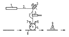
- the pressure roller 4 is rotatable in the direction of the arrow. It is assigned an electrostatic charge 6, by means of which its photoelectric coating is charged over the entire surface. This is then partially discharged again at the locations which are exposed by the laser beam 2.
- a powder application 7 arranged subsequently on the pressure roller 4 causes powdery solder to adhere to the non-discharged points of the pressure roller 4.
- the solder transfers to the circuit board 8, which is transported further to a flux application 9 in accordance with the horizontal arrows. This sprays the circuit board 8 with flux, whereby the powdered solder is fixed to the circuit board 8.
Landscapes
- Engineering & Computer Science (AREA)
- Mechanical Engineering (AREA)
- Physics & Mathematics (AREA)
- Optics & Photonics (AREA)
- Manufacturing & Machinery (AREA)
- Microelectronics & Electronic Packaging (AREA)
- Plasma & Fusion (AREA)
- Manufacturing Of Printed Wiring (AREA)
- Electric Connection Of Electric Components To Printed Circuits (AREA)
Priority Applications (1)
| Application Number | Priority Date | Filing Date | Title |
|---|---|---|---|
| EP88115726A EP0359867A1 (fr) | 1988-09-23 | 1988-09-23 | Méthode pour fabriquer des cartes à circuits imprimés électriques |
Applications Claiming Priority (1)
| Application Number | Priority Date | Filing Date | Title |
|---|---|---|---|
| EP88115726A EP0359867A1 (fr) | 1988-09-23 | 1988-09-23 | Méthode pour fabriquer des cartes à circuits imprimés électriques |
Publications (1)
| Publication Number | Publication Date |
|---|---|
| EP0359867A1 true EP0359867A1 (fr) | 1990-03-28 |
Family
ID=8199362
Family Applications (1)
| Application Number | Title | Priority Date | Filing Date |
|---|---|---|---|
| EP88115726A Withdrawn EP0359867A1 (fr) | 1988-09-23 | 1988-09-23 | Méthode pour fabriquer des cartes à circuits imprimés électriques |
Country Status (1)
| Country | Link |
|---|---|
| EP (1) | EP0359867A1 (fr) |
Cited By (1)
| Publication number | Priority date | Publication date | Assignee | Title |
|---|---|---|---|---|
| DE102006018731A1 (de) * | 2006-04-20 | 2007-11-08 | Michael Schmid | Verfahren zur Herstellung von Leiterplatten und Vorrichtung zur Durchführung des Verfahrens |
Citations (2)
| Publication number | Priority date | Publication date | Assignee | Title |
|---|---|---|---|---|
| EP0168374A2 (fr) * | 1984-07-11 | 1986-01-15 | CENTRE DE RECHERCHES METALLURGIQUES CENTRUM VOOR RESEARCH IN DE METALLURGIE Association sans but lucratif | Procédé de marquage d'un objet métallique cylindrique, tel qu'un cylindre de laminoir |
| US4604966A (en) * | 1985-10-10 | 1986-08-12 | International Business Machine Corp. | Continuous solder paste dispenser |
-
1988
- 1988-09-23 EP EP88115726A patent/EP0359867A1/fr not_active Withdrawn
Patent Citations (2)
| Publication number | Priority date | Publication date | Assignee | Title |
|---|---|---|---|---|
| EP0168374A2 (fr) * | 1984-07-11 | 1986-01-15 | CENTRE DE RECHERCHES METALLURGIQUES CENTRUM VOOR RESEARCH IN DE METALLURGIE Association sans but lucratif | Procédé de marquage d'un objet métallique cylindrique, tel qu'un cylindre de laminoir |
| US4604966A (en) * | 1985-10-10 | 1986-08-12 | International Business Machine Corp. | Continuous solder paste dispenser |
Cited By (2)
| Publication number | Priority date | Publication date | Assignee | Title |
|---|---|---|---|---|
| DE102006018731A1 (de) * | 2006-04-20 | 2007-11-08 | Michael Schmid | Verfahren zur Herstellung von Leiterplatten und Vorrichtung zur Durchführung des Verfahrens |
| DE102006018731B4 (de) * | 2006-04-20 | 2009-07-23 | Michael Schmid | Verfahren zur Herstellung von Leiterplatten mit Durchkontaktierungen und Vorrichtung zur Durchführung des Verfahrens |
Similar Documents
| Publication | Publication Date | Title |
|---|---|---|
| EP0528350B1 (fr) | Méthode de soudage et montage de composant sur plaquettes de circuits imprimés | |
| DE2944368C2 (de) | Verfahren zum Verlöten an sich nicht lötbarer Oberflächen | |
| EP0487782B1 (fr) | Méthode de soudage de plaques de circuit | |
| DE69532012T2 (de) | Einbau von Anschlussstiften in einem Substrat | |
| DE102013112348B4 (de) | Lotauftragsstempel und Verfahren zur Reparatur einer Leiterplatte mit zumindest einem defekten Bauteil | |
| DE3046341A1 (de) | Elektrische schaltungseinrichtung, sowie herstellverfahren dafuer | |
| DE4341867A1 (de) | Verfahren zum Drucken eines Verbindungsmittels | |
| DE602004009982T2 (de) | Metallschablone und Verfahren zum Drucken von bleifreier Lötpaste mit derselben | |
| DE69803664T2 (de) | Verfahren zur herstellung von gedruckten leiterplatten und so hergestellte gedruckte leiterplatten | |
| EP0594041A1 (fr) | Montage d'un écran à une plaque à circuit imprimé | |
| EP0359867A1 (fr) | Méthode pour fabriquer des cartes à circuits imprimés électriques | |
| DE19527398A1 (de) | Verfahren zum Löten von Bauelementen auf einer Trägerfolie | |
| EP3724948A1 (fr) | Procédé et dispositif de montage d'une structure d'antenne dotée d'un composant électronique | |
| DE4402545A1 (de) | Verfahren zum Ausbilden diskreter Lötstellen auf entsprechenden Kontaktanschlußflächen einer Leiterplatte | |
| DE2400665C3 (de) | Verfahren zur Herstellung eines lotabweisenden Schutzes auf Leiterplatten mit durchgehenden Lochern | |
| DE10023358A1 (de) | Fertigungslinie für die einseitige und doppelseitige Bestückung von Leiterplatten | |
| DE3445625A1 (de) | Verfahren zum loeten einer beidseitig mit smd-bauelementen bestueckten leiterbahnenplatine und eine nach diesem verfahren geloetete platine | |
| DE69609248T2 (de) | Verfahren zur Herstellung von Ladungselektroden | |
| DE1277973B (de) | Verfahren zur Herstellung einer gedruckten Schaltung | |
| EP3708938A1 (fr) | Fabrication d'une tôle magnétique | |
| DE2922304A1 (de) | Verfahren zur herstellung gedruckter schaltungen, sowie dafuer verwendete leitende farbe und vorrichtung | |
| DE102011004543A1 (de) | Impulswiderstand, Leiterplatte und elektrisches oder elektronisches Gerät | |
| EP1879435A2 (fr) | Structures électriques conductrices | |
| EP2601821A1 (fr) | Machine de sérigraphie et procédé de sérigraphie pour fabriquer des cartes de circuits imprimés pour l'industrie électrique | |
| DE102015218900A1 (de) | Verfahren und Vorrichtung zum Applizieren einer Funktionsstruktur auf einem textilen Substrat |
Legal Events
| Date | Code | Title | Description |
|---|---|---|---|
| PUAI | Public reference made under article 153(3) epc to a published international application that has entered the european phase |
Free format text: ORIGINAL CODE: 0009012 |
|
| AK | Designated contracting states |
Kind code of ref document: A1 Designated state(s): AT BE CH DE ES FR GB GR IT LI LU NL SE |
|
| RBV | Designated contracting states (corrected) |
Designated state(s): AT CH DE LI |
|
| 17P | Request for examination filed |
Effective date: 19900425 |
|
| STAA | Information on the status of an ep patent application or granted ep patent |
Free format text: STATUS: THE APPLICATION IS DEEMED TO BE WITHDRAWN |
|
| 18D | Application deemed to be withdrawn |
Effective date: 19920401 |