EP0360157B1 - Oszillator-Schaltung - Google Patents
Oszillator-Schaltung Download PDFInfo
- Publication number
- EP0360157B1 EP0360157B1 EP89117045A EP89117045A EP0360157B1 EP 0360157 B1 EP0360157 B1 EP 0360157B1 EP 89117045 A EP89117045 A EP 89117045A EP 89117045 A EP89117045 A EP 89117045A EP 0360157 B1 EP0360157 B1 EP 0360157B1
- Authority
- EP
- European Patent Office
- Prior art keywords
- circuit
- oscillation
- multivibrator
- clamping
- frequency
- Prior art date
- Legal status (The legal status is an assumption and is not a legal conclusion. Google has not performed a legal analysis and makes no representation as to the accuracy of the status listed.)
- Expired - Lifetime
Links
- 230000010355 oscillation Effects 0.000 title claims description 77
- 239000003990 capacitor Substances 0.000 claims description 23
- 238000009499 grossing Methods 0.000 claims description 9
- 238000010586 diagram Methods 0.000 description 7
- 238000007599 discharging Methods 0.000 description 3
- 239000013078 crystal Substances 0.000 description 1
- 230000001419 dependent effect Effects 0.000 description 1
- 238000011161 development Methods 0.000 description 1
- 230000018109 developmental process Effects 0.000 description 1
- 230000002452 interceptive effect Effects 0.000 description 1
- 238000000034 method Methods 0.000 description 1
- 230000006641 stabilisation Effects 0.000 description 1
- 238000011105 stabilization Methods 0.000 description 1
- 230000000087 stabilizing effect Effects 0.000 description 1
Images

Classifications
-
- H—ELECTRICITY
- H03—ELECTRONIC CIRCUITRY
- H03B—GENERATION OF OSCILLATIONS, DIRECTLY OR BY FREQUENCY-CHANGING, BY CIRCUITS EMPLOYING ACTIVE ELEMENTS WHICH OPERATE IN A NON-SWITCHING MANNER; GENERATION OF NOISE BY SUCH CIRCUITS
- H03B5/00—Generation of oscillations using amplifier with regenerative feedback from output to input
- H03B5/20—Generation of oscillations using amplifier with regenerative feedback from output to input with frequency-determining element comprising resistance and either capacitance or inductance, e.g. phase-shift oscillator
- H03B5/24—Generation of oscillations using amplifier with regenerative feedback from output to input with frequency-determining element comprising resistance and either capacitance or inductance, e.g. phase-shift oscillator active element in amplifier being semiconductor device
-
- H—ELECTRICITY
- H03—ELECTRONIC CIRCUITRY
- H03C—MODULATION
- H03C3/00—Angle modulation
- H03C3/02—Details
- H03C3/09—Modifications of modulator for regulating the mean frequency
-
- H—ELECTRICITY
- H03—ELECTRONIC CIRCUITRY
- H03L—AUTOMATIC CONTROL, STARTING, SYNCHRONISATION OR STABILISATION OF GENERATORS OF ELECTRONIC OSCILLATIONS OR PULSES
- H03L7/00—Automatic control of frequency or phase; Synchronisation
- H03L7/06—Automatic control of frequency or phase; Synchronisation using a reference signal applied to a frequency- or phase-locked loop
- H03L7/08—Details of the phase-locked loop
- H03L7/0805—Details of the phase-locked loop the loop being adapted to provide an additional control signal for use outside the loop
-
- H—ELECTRICITY
- H03—ELECTRONIC CIRCUITRY
- H03L—AUTOMATIC CONTROL, STARTING, SYNCHRONISATION OR STABILISATION OF GENERATORS OF ELECTRONIC OSCILLATIONS OR PULSES
- H03L7/00—Automatic control of frequency or phase; Synchronisation
- H03L7/06—Automatic control of frequency or phase; Synchronisation using a reference signal applied to a frequency- or phase-locked loop
- H03L7/08—Details of the phase-locked loop
- H03L7/099—Details of the phase-locked loop concerning mainly the controlled oscillator of the loop
Definitions
- the present invention relates generally to oscillation circuits adaptable to FM modulation circuits employed in home VTR (Video Tape Recorders) and the like.
- the luminance signal is clamped in a clamping circuit to make uniform direct current peak levels of a synchronizing signal thereof, and the clamped luminance signal is then FM modulated in an FM modulation circuit.
- This FM modulation circuit generally comprises an astable multivibrator. This astable multivibrator oscillates at a carrier frequency in a synchronizing signal period, but has an oscillation frequency changing depending on the level of the luminance signal in the other periods.
- the described carrier frequency is, for example, set at 3.4MHz in a VHS system, but is generally required to have high accuracy.
- the FM modulation circuit in an IC (an integrated circuit)
- stabilization of the carrier frequency is attempted by adjusting a variable resistor which is externally provided to the IC.
- the external variable resistor also adjusts a deviation range of the oscillation frequency.
- Such an FM modulation circuit is, for example, disclosed in Japanese Utility Model Laying-Open No. 60-150865.
- An oscillation circuit comprising a first multivibrator and a second multivibrator having the same configuration as the first multivibrator, is configured such that an oscillation output signal of the second multivibrator is compared in phase with that of a reference oscillation circuit so as to control the oscillation frequencies of the first and second multivibrators in accordance with the difference in phase between these oscillation output signals.
- a PLL Phase Locked Loop
- capacitors for oscillation frequency control are provided to the first and second multivibrators, respectively.
- first and second transistors are provided on respective paths of a control current to be supplied to the first and second multivibrators.
- a clamping circuit is provided to clamp the luminance signal in the video signal, and a voltage corresponding to a reference voltage for clamping of this clamping circuit is applied to the respective bases of the first and second transistors.
- a third resistor is provided to adjust a deviation range of the oscillation frequency of the first multivibrator. The third resistor has one end connected to the emitter of the first transistor and the other end supplied with an output signal of the clamping circuit.
- the first multivibrator has its oscillation frequency also adjusted in the same manner as the second multivibrator has, so that an oscillation output signal with a desired frequency can be obtained from the first multivibrator.
- the first multivibrator can be operated as an FM modulation circuit for FM modulating the luminance signal.
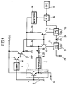
- a clamping circuit 1 comprises a transistor 3 having a base connected to a reference power supply 2 and a collector supplied with a supply voltage +Vcc, and a capacitor 4 having one electrode connected to the emitter of the transistor 3 and the other electrode connected to an input terminal 5.
- This clamping circuit 1 clamps a luminance signal to be applied to the input terminal 5.
- the luminance signal outputted from the clamping circuit 1 is applied to an emphasis circuit 6 to be subject to emphasis.
- a dummy circuit 7 is supplied with a reference voltage from the reference power supply 2.
- the dummy circuit 7 is configured to have the same response of a direct current level as that of the emphasis circuit 6.
- An output of the dummy circuit 7 is applied to the base of a transistor 8.
- the transistor 8 has the collector supplied with the supply voltage +Vcc. Further, the emitter of the transistor 8 is connected to the base of a transistor 9 and is also grounded via a resistor.
- the transistor 9 has the collector supplied with the supply voltage +Vcc. The emitter of the transistor 9 is connected to the respective bases of the first transistor 10 and the second transistor 11, and is also grounded via a resistor.
- the transistors 8 and 9 form a level shifting circuit for shifting the level of an output voltage of the dummy circuit 7 by a predetermined value. An output voltage of the level shifting circuit is applied to the respective bases of the first and second transistors 10 and 11.
- a first multivibrator 12 having a first capacitor 13 has its oscillation frequency determined by a capacitance value of this capacitor 13 and by a control current from the collector of the first transistor 10.
- the first multivibrator 12 operates as an FM modulation circuit of a VTR.
- a second multivibrator 14 having a second capacitor 15 has its oscillation frequency determined by a capacitance value of this second capacitor 15 and by a control current from the collector of the second transistor 11.
- a phase comparing circuit 16 compares in phase an oscillation output signal of the second multivibrator 14 with that of a fixed oscillation circuit 17.
- a smoothing circuit 18 smoothes an error output of the phase comparing circuit 16.
- a first resistor 19 and a second resistor 20 are connected between the respective emitters of the first and second transistors 10 and 11 and an output terminal of the smoothing circuit 18.
- the first and second resistors 19 and 20 are selected to have the same resistance values.
- a variable resistor 21 is connected between an output terminal A of the emphasis circuit 6 and an emitter terminal B of the first transistor 10.
- the variable resistor 21 serves to set a deviation range of the oscillation frequency of the first multivibrator 12.
- the luminance signal from the input terminal 5 is clamped in the clamping circuit 1 so that the peak of its synchronizing signal have a fixed value of a direct current level.
- a reference voltage of the reference power supply 2 is Vref
- a luminance signal whose synchronizing signal has a peak level of Vref-V BE (the V BE is a voltage developed across the base and emitter of the transistor 3), is applied from the emitter of the transistor 3 to the emphasis circuit 6.
- a direct current potential difference between input and output of the emphasis circuit 6 is ⁇ V
- a direct current potential difference between input and output of the dummy circuit 7, to which the reference voltage Vref is applied from the reference power supply 2 of the clamping circuit 1 is set equally to the ⁇ V. Accordingly, a constant voltage (Vref + ⁇ V - 2V BE ) is developed at the emitter of the transistor 9 and applied to the respective bases of the first and second transistors 10 and 11. Therefore, a direct current voltage (Vref + ⁇ V - V BE ) is developed at the emitter of the first transistor 10.
- a voltage on the terminal A (the output terminal of the emphasis circuit 6) in a synchronizing signal period attains the value of Vref + ⁇ V - V BE , which is equal to a voltage on the terminal B (the emitter of the first transistor 10). Accordingly, no current flows through the variable resistor 21, and only a current from the first resistor 19 flows in the emitter of the first transistor 10.
- An output voltage smoothed in the smoothing circuit 18 is then applied to one terminal of the second resistor 20, so that a current corresponding to the value of the output voltage of the smoothing circuit 18 flows through an emitter-collector path of the second transistor 11.
- the current flowing through the emitter-collector path of the second transistor 11 is supplied as a control current to the second multivibrator 14. Therefore, the second multivibrator 14 can oscillate at the same frequency as that of the fixed oscillation circuit 17.
- the home VTR comprises a low frequency converting circuit for converting a frequency of a chroma signal, and includes an oscillation circuit oscillating at a fixed frequency of 3.58MHz.
- the above oscillation circuit oscillates based on a crystal resonator and thus is very stable. Therefore, it is possible to employ as the fixed oscillation circuit 17 the oscillation circuit included in the above described low frequency converting circuit.
- the output voltage of the smoothing circuit 18 is also applied to one end of the first resistor 19, a current equivalent to the current flowing in the second transistor 11 also flows through the emitter-collector path of the first transistor 10.
- This current flowing in the first transistor 10 is supplied to the first multivibrator 12. Therefore, the first multivibrator 12 is controlled in the same manner as the second multivibrator 14, thereby stabilizing the oscillation frequency thereof.
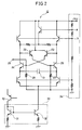
- Fig. 2 is a circuit diagram illustrating a detailed circuit example of the first multivibrator 12 shown in Fig. 1, which is, for example, disclosed in Japanese Patent Publication No. 59-30337. It should be pointed out here that the second multivibrator 14 has approximately the same configuration as that of the first multivibrator 12 which will be described as follows with reference to Fig. 2.
- an emitter-coupled astable multivibrator portion is formed of transistors 22, 23, 24 and 25, and a capacitor 13. That is, a collector output of the transistor 24 is applied to the base of the transistor 25 via an emitter follower formed of the transistor 22 and a resistor 27.
- a collector output of the transistor 25 is applied to the base of the transistor 24 via an emitter follower formed of the transistor 23 and a resistor 28.
- the respective emitters of the transistors 24 and 25 are connected to each other via the capacitor 13 for charging/discharging. This configuration enables the transistors 24 and 25 to be conductive alternately and then the charging/discharging capacitor 13 to be charged/discharged, resulting in a predetermined oscillation output signal at an output terminal 29.
- a current flowing from the collector of the first transistor 10 (equivalent to the corresponding one in Fig. 1) is supplied to an input of a current mirror circuit 33 formed of transistors 31 and 32. Accordingly, a current which is equivalent to the collector current of the first transistor 10 flows in the collector of the transistor 32, so that the oscillation frequency of the astable multivibrator is controlled.
- the I1 represents a collector current of the transistor 32; the C1 is the capacitance value of the charging/discharging capacitor 13; and the ⁇ V is a difference voltage between points a and b in a bias source 34.
- the difference voltage ⁇ V is a constant value in the expression (1)
- the oscillation frequency F1 is expressed as follows. F1 ⁇ I1/C1
- the oscillation frequency F1 of the oscillation circuit shown in Fig. 2 is determined in accordance with the current I1 and the capacitance value C1.
- the I1 and I2 represent collector currents of the first and second transistors 10 and 11, and the C1 and C2 represent capacitance values of the first and second capacitors 13 and 15, respectively.
- the oscillation frequency F1 of the first multivibrator 12 can be set arbitrarily in accordance with a ratio of the capacitor C1 to C2.
- a carrier frequency of the first multivibrator 12 can automatically be adjusted to a constant value during the synchronizing signal period of a luminance signal. Since the voltage (Vref - V BE + ⁇ V) in the synchronizing signal period at the terminal A is set equally to a voltage developed in no-signal inputting (a state that a bias due to the power supply is only applied to each of the transistors rather than the luminance signal is) of the oscillation circuit in Fig. 1, the first multivibrator 12 is controlled even in no-signal inputting.
- the value of the oscillation frequency F1 may be adjusted by equally setting the respective capacitance values C1 and C2 of the capacitors 13 and 15 and by changing the ratio of the collector current I1 to I2.
- the values of the first and second resistors 19 and 20 in Fig. 1 may be adjusted.
- a luminance signal in the other periods than the synchronizing signal period is developed at the terminal A.
- this luminance signal is generated at the terminal A, a potential difference occurs between both ends of the variable resistor 21, and thus a current corresponding to this potential difference flows in the emitter of the first transistor 10 to be supplied to the first multivibrator 12 via the collector thereof.
- the first multivibrator 12 has its oscillation frequency changed in accordance with the level of the luminance signal, resulting in an FM modulated luminance signal at the output terminal 29.
- the bias source 34 shown in Fig. 1 is, for example, formed of a voltage dividing circuit comprising a plurality of resistors connected in series between the power supply +Vcc and the ground such as the bias source 34 shown in Fig. 2.
- a bias voltage is applied from the same bias source 34 to the first and second multivibrators 12 and 14. Accordingly, the ⁇ V in the expression (1) can be set to be completely the same values, resulting in further enhanced accuracy in frequency setting.
- Fig. 3 is a circuit diagram illustrating a detailed circuit example of the emphasis circuit 6 shown in Fig. 1.
- a luminance signal from an input terminal 35 is applied to the base of a transistor 37 and then applied to an emphasis portion 36 from the emitter thereof to be subject to emphasis.
- the emphasized luminance signal is provided to an output terminal 39 via a transistor 38 for level shifting.
- Fig. 4 is a circuit diagram illustrating a detailed circuit example of a dummy circuit 7 shown in Fig. 1.
- the dummy circuit 7 shown in Fig. 4 has the same configuration as that of the emphasis circuit 6 shown in Fig. 3 except the point that the circuit 7 does not include the capacitor for emphasis. That is, the circuit of Fig. 4 is the one having the resistors, with the capacitor removed from the emphasis portion 36 in Fig. 3. Accordingly, the dummy circuit 7 of Fig. 4 has the same direct current level change as that of the emphasis circuit 6 of Fig. 3. Therefore, the terminals A and B shown in Fig. 1 can have completely the same direct current levels.
- the carrier frequency of the oscillation circuit can be adjusted automatically.
- the oscillation frequency (the carrier frequency) of the first multivibrator can be adjusted such as by a capacitance ratio of these two multivibrators.
- setting of this capacitance ratio to a desired value results in an oscillation output signal of high accuracy.
Landscapes
- Television Signal Processing For Recording (AREA)
- Stabilization Of Oscillater, Synchronisation, Frequency Synthesizers (AREA)
- Picture Signal Circuits (AREA)
Claims (6)
- Oszillationsschaltung mit:
einem ersten Multivibrator (12), dessen Frequenz stromgesteuert ist,
einem zweiten Multivibrator (14), dessen Frequenz stromgesteuert ist und der dieselbe Schaltungsgestaltung wie der erste Multivibrator aufweist, und
einer Bezugsoszillationsschaltung (17), die mit einer konstanten Frequenz oszilliert,
gekennzeichnet durch ferner:
eine Phasenvergleichsschaltung (16) zum Phasenvergleichen eines Oszillations-Ausgangssignals der Bezugsoszillationsschaltung mit dem des zweiten Multivibrators und
eine Glättungsschaltung (18) zum Glätten des Ausgangssignals der Phasenvergleichsschaltung zum Zuführen des geglätteten Ausgangssignals an den ersten und an den zweiten Multivibrator (12, 14) als Steuerstrom zur Bestimmung einer Oszillationsfrequenz,
wodurch die Oszillationsfrequenz des ersten Multivibrators (12) stabilisiert wird. - Oszillationsschaltung nach Anspruch 1,
wobei
der erste Multivibrator (12) einen ersten Kondensator (13) aufweist und seine Oszillationsfrequenz durch die Kapazität des ersten Kondensators und durch einen Steuerstrom gesteuert wird,
der zweite Multivibrator (14) einen zweiten Kondensator (15) aufweist und seine Oszillationsfrequenz durch die Kapazität des zweiten Kondensators und durch einen Steuerstrom gesteuert wird,
wobei die Oszillationsfrequenz des ersten Multivibrators entsprechend dem Kapazitätsverhältnis des ersten Kondensators und des zweiten Kondensators eingestellt werden kann. - Oszillationsschaltung nach Anspruch 2 mit ferner: einer Klemmschaltung (1) zum Festklemmen eines Luminanzsignals eines Videosignals,
einem ersten und einem zweiten Transistor (10, 11), deren Basen mit einer Spannung versorgt werden, die einer Bezugsspannung zum Klemmen der Klemmschaltung (1) entspricht,
einem ersten und einem zweiten Widerstand (19, 20), die zwischen die Emitter des ersten und des zweiten Transistors (10, 11) und einen Ausgangsanschluß der Glättungsschaltung (18) geschaltet sind, und
einem dritten Widerstand (21), dessen eines Ende mit dem Emitter des ersten Transistors (10) verbunden ist und dessen anderes Ende mit einem Ausgangssignal der Klemmschaltung (1) versorgt wird,
wobei ein Kollektorstrom des ersten und des zweiten Transistors (10, 11) als Steuerstrom dem ersten und dem zweiten Multivibrator (12, 14) zugeführt wird, und
einem Ausgangsanschluß des ersten Multivibrators (12), der ein Oszillations-Ausgangssignal liefert, dessen Oszillationsfrequenz sich in Übereinstimmung mit einem Luminanzsignal ändert. - Oszillationsschaltung nach Anspruch 3,
mit ferner:
einer Verstärkungsschaltung (6) zum Verstärken eines Luminanzsignales von der Klemmschaltung (1),
einer Pseudoschaltung (7), die mit einer Bezugsspannung zum Klemmen der Klemmschaltung (1) versorgt wird und dieselbe Gleichstromfluktuation wie die Verstärkungsschaltung (6) aufweist. - Oszillationsschaltung nach Anspruch 3 oder 4, wobei der Widerstandswert des ersten Widerstandes (19) auf den gleichen Wert wie der zweite Widerstand (20) eingestellt wird.
- Oszillationsschaltung nach Anspruch 3 oder 4, wobei der erste und der zweite Widerstand (19, 20) jeweils feste Widerstände aufweisen und der dritte Widerstand (21) einen variablen Widerstand aufweist.
Applications Claiming Priority (2)
| Application Number | Priority Date | Filing Date | Title |
|---|---|---|---|
| JP63234124A JPH0282719A (ja) | 1988-09-19 | 1988-09-19 | 発振回路 |
| JP234124/88 | 1988-09-19 |
Publications (3)
| Publication Number | Publication Date |
|---|---|
| EP0360157A2 EP0360157A2 (de) | 1990-03-28 |
| EP0360157A3 EP0360157A3 (en) | 1990-09-19 |
| EP0360157B1 true EP0360157B1 (de) | 1995-01-11 |
Family
ID=16966011
Family Applications (1)
| Application Number | Title | Priority Date | Filing Date |
|---|---|---|---|
| EP89117045A Expired - Lifetime EP0360157B1 (de) | 1988-09-19 | 1989-09-14 | Oszillator-Schaltung |
Country Status (6)
| Country | Link |
|---|---|
| US (1) | US4918407A (de) |
| EP (1) | EP0360157B1 (de) |
| JP (1) | JPH0282719A (de) |
| KR (1) | KR960008284B1 (de) |
| DE (1) | DE68920522T2 (de) |
| ES (1) | ES2069559T3 (de) |
Families Citing this family (1)
| Publication number | Priority date | Publication date | Assignee | Title |
|---|---|---|---|---|
| CA2955201A1 (en) * | 2014-07-18 | 2016-01-21 | The Procter & Gamble Company | Absorbent catamenial tampon |
Family Cites Families (5)
| Publication number | Priority date | Publication date | Assignee | Title |
|---|---|---|---|---|
| JPS5636613B2 (de) * | 1974-01-29 | 1981-08-25 | ||
| JPS5665530A (en) * | 1979-10-31 | 1981-06-03 | Sony Corp | Pll circuit |
| US4494080A (en) * | 1981-11-16 | 1985-01-15 | International Business Machines Corporation | Voltage-controlled oscillator with independent gain and frequency controls |
| JPS60150865U (ja) * | 1984-03-19 | 1985-10-07 | 三洋電機株式会社 | 周波数及び周波数偏移調整回路 |
| JPS61281623A (ja) * | 1985-05-09 | 1986-12-12 | Sanyo Electric Co Ltd | 発振周波数調整装置 |
-
1988
- 1988-09-19 JP JP63234124A patent/JPH0282719A/ja active Pending
-
1989
- 1989-09-14 ES ES89117045T patent/ES2069559T3/es not_active Expired - Lifetime
- 1989-09-14 DE DE68920522T patent/DE68920522T2/de not_active Expired - Fee Related
- 1989-09-14 EP EP89117045A patent/EP0360157B1/de not_active Expired - Lifetime
- 1989-09-14 US US07/407,188 patent/US4918407A/en not_active Expired - Lifetime
- 1989-09-18 KR KR1019890013363A patent/KR960008284B1/ko not_active Expired - Fee Related
Also Published As
| Publication number | Publication date |
|---|---|
| DE68920522D1 (de) | 1995-02-23 |
| ES2069559T3 (es) | 1995-05-16 |
| DE68920522T2 (de) | 1995-08-31 |
| JPH0282719A (ja) | 1990-03-23 |
| EP0360157A3 (en) | 1990-09-19 |
| EP0360157A2 (de) | 1990-03-28 |
| KR900005681A (ko) | 1990-04-14 |
| KR960008284B1 (ko) | 1996-06-21 |
| US4918407A (en) | 1990-04-17 |
Similar Documents
| Publication | Publication Date | Title |
|---|---|---|
| US4494080A (en) | Voltage-controlled oscillator with independent gain and frequency controls | |
| EP0595632A2 (de) | Phasensynchronisierungsschaltungen | |
| US5534943A (en) | Frequency modulation system having control of a carrier frequency | |
| JPS6224974B2 (de) | ||
| EP0357996A1 (de) | Einen Synthesierer verwendender Frequenzmodulator | |
| US5164685A (en) | Phase-locked loop with circuit for adjusting a phase comparator's output amplitude | |
| US6476684B2 (en) | Low noise frequency modulator having variable carrier frequency | |
| US5751194A (en) | Phase-locked loop having charge pump controlled according to temperature and frequency | |
| EP0360157B1 (de) | Oszillator-Schaltung | |
| US4544897A (en) | Crystal oscillator circuit with feedback control | |
| EP0325394A2 (de) | Sender mit PLL-Schaltung | |
| JPH06224642A (ja) | Fm変調器の周波数調整回路 | |
| US4806883A (en) | Multifrequency oscillator circuit | |
| KR940011376B1 (ko) | Vtr의 캐리어 주파수 자동 조정 회로 | |
| US6404292B1 (en) | Voltage controlled oscillators with reduced incidental frequency modulation and use in phase locking oscillators | |
| JP3326286B2 (ja) | Pll周波数シンセサイザ回路 | |
| CA1327064C (en) | Phase-locked loop circuit | |
| EP0555001A1 (de) | FM Demodulatorschaltung | |
| KR0151100B1 (ko) | 다중 동기용 수평 전압 제어 발진 회로 | |
| JPH0787368B2 (ja) | 外部制御型原子発振器 | |
| US4528527A (en) | SECAM Modulator | |
| JPH05110432A (ja) | Pll周波数シンセサイザ | |
| JP3033049B2 (ja) | Dcfm回路の周波数ドリフト補正回路 | |
| JPS60218920A (ja) | 位相同期回路 | |
| JPH0722841A (ja) | 電圧制御発振器 |
Legal Events
| Date | Code | Title | Description |
|---|---|---|---|
| PUAI | Public reference made under article 153(3) epc to a published international application that has entered the european phase |
Free format text: ORIGINAL CODE: 0009012 |
|
| AK | Designated contracting states |
Kind code of ref document: A2 Designated state(s): DE ES FR GB |
|
| PUAL | Search report despatched |
Free format text: ORIGINAL CODE: 0009013 |
|
| AK | Designated contracting states |
Kind code of ref document: A3 Designated state(s): DE ES FR GB |
|
| 17P | Request for examination filed |
Effective date: 19900919 |
|
| 17Q | First examination report despatched |
Effective date: 19921109 |
|
| GRAA | (expected) grant |
Free format text: ORIGINAL CODE: 0009210 |
|
| AK | Designated contracting states |
Kind code of ref document: B1 Designated state(s): DE ES FR GB |
|
| REF | Corresponds to: |
Ref document number: 68920522 Country of ref document: DE Date of ref document: 19950223 |
|
| ET | Fr: translation filed | ||
| REG | Reference to a national code |
Ref country code: ES Ref legal event code: FG2A Ref document number: 2069559 Country of ref document: ES Kind code of ref document: T3 |
|
| PLBE | No opposition filed within time limit |
Free format text: ORIGINAL CODE: 0009261 |
|
| STAA | Information on the status of an ep patent application or granted ep patent |
Free format text: STATUS: NO OPPOSITION FILED WITHIN TIME LIMIT |
|
| 26N | No opposition filed | ||
| REG | Reference to a national code |
Ref country code: GB Ref legal event code: IF02 |
|
| PGFP | Annual fee paid to national office [announced via postgrant information from national office to epo] |
Ref country code: FR Payment date: 20030909 Year of fee payment: 15 |
|
| PGFP | Annual fee paid to national office [announced via postgrant information from national office to epo] |
Ref country code: GB Payment date: 20030910 Year of fee payment: 15 |
|
| PGFP | Annual fee paid to national office [announced via postgrant information from national office to epo] |
Ref country code: DE Payment date: 20030925 Year of fee payment: 15 |
|
| PGFP | Annual fee paid to national office [announced via postgrant information from national office to epo] |
Ref country code: ES Payment date: 20031021 Year of fee payment: 15 |
|
| PG25 | Lapsed in a contracting state [announced via postgrant information from national office to epo] |
Ref country code: GB Free format text: LAPSE BECAUSE OF NON-PAYMENT OF DUE FEES Effective date: 20040914 |
|
| PG25 | Lapsed in a contracting state [announced via postgrant information from national office to epo] |
Ref country code: ES Free format text: LAPSE BECAUSE OF NON-PAYMENT OF DUE FEES Effective date: 20040915 |
|
| PG25 | Lapsed in a contracting state [announced via postgrant information from national office to epo] |
Ref country code: DE Free format text: LAPSE BECAUSE OF NON-PAYMENT OF DUE FEES Effective date: 20050401 |
|
| GBPC | Gb: european patent ceased through non-payment of renewal fee |
Effective date: 20040914 |
|
| PG25 | Lapsed in a contracting state [announced via postgrant information from national office to epo] |
Ref country code: FR Free format text: LAPSE BECAUSE OF NON-PAYMENT OF DUE FEES Effective date: 20050531 |
|
| REG | Reference to a national code |
Ref country code: FR Ref legal event code: ST |
|
| REG | Reference to a national code |
Ref country code: ES Ref legal event code: FD2A Effective date: 20040915 |