EP0360672A1 - Piezoelektrisches monolithisches Filter mit modifizierter Selektivität - Google Patents
Piezoelektrisches monolithisches Filter mit modifizierter Selektivität Download PDFInfo
- Publication number
- EP0360672A1 EP0360672A1 EP89402537A EP89402537A EP0360672A1 EP 0360672 A1 EP0360672 A1 EP 0360672A1 EP 89402537 A EP89402537 A EP 89402537A EP 89402537 A EP89402537 A EP 89402537A EP 0360672 A1 EP0360672 A1 EP 0360672A1
- Authority
- EP
- European Patent Office
- Prior art keywords
- electrode
- filter
- cell
- circuits
- circuit
- Prior art date
- Legal status (The legal status is an assumption and is not a legal conclusion. Google has not performed a legal analysis and makes no representation as to the accuracy of the status listed.)
- Withdrawn
Links
- 239000000835 fiber Substances 0.000 title 1
- 239000003990 capacitor Substances 0.000 claims abstract description 11
- 230000015572 biosynthetic process Effects 0.000 description 23
- 238000003786 synthesis reaction Methods 0.000 description 23
- 230000002238 attenuated effect Effects 0.000 description 13
- 238000010586 diagram Methods 0.000 description 8
- 230000008878 coupling Effects 0.000 description 6
- 238000010168 coupling process Methods 0.000 description 6
- 238000005859 coupling reaction Methods 0.000 description 6
- 230000006978 adaptation Effects 0.000 description 4
- 238000005259 measurement Methods 0.000 description 2
- 238000000034 method Methods 0.000 description 2
- 230000001808 coupling effect Effects 0.000 description 1
- 230000000593 degrading effect Effects 0.000 description 1
- 239000006185 dispersion Substances 0.000 description 1
- 230000000694 effects Effects 0.000 description 1
- 238000001914 filtration Methods 0.000 description 1
- 230000001939 inductive effect Effects 0.000 description 1
- 238000004519 manufacturing process Methods 0.000 description 1
- 239000000463 material Substances 0.000 description 1
- 230000003071 parasitic effect Effects 0.000 description 1
- 230000003313 weakening effect Effects 0.000 description 1
- 238000004804 winding Methods 0.000 description 1
Images


Classifications
-
- H—ELECTRICITY
- H03—ELECTRONIC CIRCUITRY
- H03H—IMPEDANCE NETWORKS, e.g. RESONANT CIRCUITS; RESONATORS
- H03H9/00—Networks comprising electromechanical or electro-acoustic elements; Electromechanical resonators
- H03H9/46—Filters
- H03H9/54—Filters comprising resonators of piezoelectric or electrostrictive material
- H03H9/542—Filters comprising resonators of piezoelectric or electrostrictive material including passive elements
Definitions
- the invention proposes to improve the selectivity of such filters.
- a monolithic cell consists of two resonators mechanically coupled on the same blade of piezoelectric material. On one face of this blade there are first and second opposite electrodes separated from each other by a small distance. On the other side there is a third electrode common to the two resonators. This third electrode can also consist of two electrodes connected to each other. This third electrode is generally a ground electrode.
- the number of resonators used in a filter fixes the number of poles of the filter.
- the synthesis curve giving the attenuation (in decibels) as a function of the frequency of the filter must be written inside and / or outside the templates.
- the selectivity of a filter is defined by its form factor K which is the ratio:
- K which is the ratio:
- the attenuated band corresponds to the width of the frequency band measured on the synthesis curve a YdB below its maximum.
- the value of Y is, for example, -45 decibels.
- the passband corresponds to the width of the frequency band measured on the synthesis curve at XdB below its maximum.
- the value of X is, for example, -3 decibels. The higher the selectivity of a filter, the lower its form factor and the steeper the sides of the synthesis curve.
- a piezoelectric filter with N poles using a succession of n monolithic cells (Y1, Y2, ..., Y i ..., Y n ) (with n N / 2) connected in cascade, of known type is shown in the figure 1.
- the input of the filter is done on an active terminal E and the output on an active terminal S.
- Each monolithic cell (Y1, Y2, ... Y i , ..., Y n ) essentially comprises a first electrode 1, a second electrode 2 and a third electrode 3 common. The third electrode is grounded.
- This filter is inserted between a source of electromotive force e, internal resistance Znat and a load Z′nat. He is cordoned off on his natural impedance. It has a central frequency F o .
- Tuning circuits A i with the number of n + 1 are inserted in the filter circuit.
- the second electrode 2 of a cell Y i is connected on the one hand to a first end of one of the tuning circuits A i + 1 and on the other hand to the first electrode 1 of the next cell Y i + 1 .
- the first electrode 1 of the first cell Y1 is connected on the one hand to a first end of the first tuning circuit A1 and on the other hand to the input terminal E.
- the second electrode 2 of the last cell Y n is connected on the one hand to the first end of the last tuning circuit A n + 1 and on the other hand to the output terminal S.
- the second ends of the tuning circuits (A1 ... A n + 1 ) are grounded.
- the tuning circuits can consist of either a capacitor, an inductor, or with a capacity and an inductor connected in parallel.
- the circuits (A1 ... A n + 1 ) are not all of the same type. All combinations are possible.
- the synthesis curve of such a filter hereinafter called the original filter, is symmetrical and monotonous. It has sides quite distant from the vertical and the attenuated strip points are often too close to the gauge, if one wishes to take into account the thermal drift and manufacturing dispersions of the filter components. The selectivity of such a filter is not good.
- FIG. 2 Another known method for obtaining a steeper synthesis curve consists in artificially unbalancing the original filter by clamping it.
- a flanged filter is shown in Figure 2. Its diagram is comparable to the original filter shown in Figure 1, but a capacitor C B was added in parallel between the first electrode 1 and the second electrode 2 of at least one cells Y i .
- the introduction of the capacitance C B creates on the synthesis curve minima or infinite attenuation points situated in the attenuated band.
- FIG. 3 we find all the components of an original filter and / or an N-pole flanged filter described previously in FIGS. 1 and 2. These components have the same references as in FIGS. 1 and 2.
- the filter also comprises a succession of n first circuits C i .
- Each circuit C i is inserted between the common electrode (3) of a cell Y i and the ground.
- the first circuits C i are preferably each composed of a capacity (C1), (C2)), ..., (C i ), ..., (C n ).
- the capacitance values (C i ) will be chosen so as to obtain a compromise between the amplitude of the infinite attenuation peaks and the offset of the low frequency.
- the offset of the low frequency can be canceled by choosing after the first measurements of the monolithic cells (Y i ) whose low frequency is corrected accordingly.
- the filter also includes a succession of second circuits (L 1i , C 1i ). Each of these second circuits (L 1i , C 1i ) is inserted between the common electrode 3 of a first cell Y i and the common electrode 3 of the next cell Y i + 1 . There are n-1 second circuits (L 1i , C 1i ) and they are each composed of an inductance L 1i and a capacity C 1i connected in parallel. These n-1 second circuits (L 1i C 1i ) are tuned near the central frequency F o of the filter. They measure the coupling between two consecutive cells (Y i , Y i + 1 ) They cancel the various existing couplings between the components of the filter.
- the measurements show that there are several values for the capacitance C 1i and that there is an optimum value which corresponds on the synthesis curve to the minimum ascent in the out-of-band area.
- the filter finally comprises a succession of third circuits (L 2i , C 2i ). Each of these third circuits is inserted between the common electrode 3 and the second electrode 2 of the last n-1 cells Y i . There are n-1 third circuits. They each consist of an inductor L 2i and a capacitor C 2i connected in parallel.
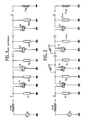
- FIG. 4 represents an electrical diagram of a variant of a filter according to the invention.
- the difference between the filter shown in Figure 3 and the one shown in Figure 4 comes from the position of the third circuits (L ′ 2i , C ′ 2i ).
- each of the third circuits (L ′ 2i , C ′ 2i ) is inserted between the common electrode 3 and the first electrode 1 of the first n-1 cells Y 2i .
- Each of the third circuits (L ′ 2i , C ′ 2i ) is composed as before of an inductance L ′ 2i and a capacitor C ′ 2i connected in parallel.
- n-1 third circuits (L 2i , C 2i ) or (L ′ 2i , C ′ 2i ) are tuned near the center frequency F o of the filter. They cancel the voltage present across the capacitors C i .
- FIG. 5 represents the diagram of a filter according to the invention with 4 poles. There are two monolithic cells Y1, Y2, three tuning circuits A1, A2, A3.
- the tuning circuit A1 consists of an inductance L A1 .
- the tuning circuit A2 consists of a capacitor C A2 .
- the tuning circuit A3 consists of a capacity C A3 .
- Other combinations could have been used for the tuning circuits in particular it could have been envisaged that one of them would consist of an LC circuit in parallel.
- a capacitor C B is placed in parallel between the first electrode 1 and the second electrode 2 of the cell Y2.
- the circuit also includes a capacity C1 between the common electrode 3 of the cell Y1 and the ground and a capacity C2 between the common electrode Y2 and the ground.
- a parallel L11C11 circuit is inserted between the common electrode 3 of the cell Y1 and the common electrode 3 of the cell Y2.
- a parallel L22C22 circuit is inserted between the common electrode 3 and the second electrode 2 of the cell Y2.
- the filter shown is now adapted.
- the adaptation shown is a high pass adaptation.
- the impedance Znat has been replaced by a resistor R or impedance of adaptation in series with a capacitance C. The same is true for the impedance Z′nat.
- FIG. 6 represents the synthesis curve of an original filter, of a flanged filter and of a filter according to the invention around the passband.
- the three filters have four poles and the filter according to the invention corresponds to the filter described in FIG. 5.
- the synthesis curve represents the attenuation A of the filter in decibels as a function of the frequency F in kHz.
- the curves shown are centered on the central frequency F o of the filter.
- the curve of the original filter is marked I.
- the curve of the flanged filter bears the mark II.
- a template 60 is shown at -3dB on either side of the central frequency. It indicates that the minimum bandwidth of the filter must be greater than or equal to 60 kHz.
- the bandwidth of the original filter (see curve I) is less than the template 60.
- FIG. 7 represents the synthesis curve of the same filters as above around the band attenuated at -45dB.
- the curves bear the same references as in FIG. 5.
- the template placed at -45dB bears the reference 70.
- the attenuated band must be less than or equal to 200 kHz.
- curve 1 The sides of curve 1 are quite far from the vertical while those of curves II and III are steeper.
- the attenuated band points 71 of the curve I are very close to the template 70.
- the curve II of the flanged filter has at least one infinite attenuation tip 72. This tip 72 comes from the introduction of the capacities C B. Curve II presents only one point 72 because only one capacity C B has been added, the filter considered having only two monolithic cells Y1, Y2.
- Curve III of the filter according to the invention has several infinite attenuation tips 73. These peaks come from both the capacity C B and the capacities C enters and C2.
- Figure 8 shows, as before, the synthesis curves in the out-of-band area.
- the mask placed at -50dB carries the reference 80.
- the out-of-band loss is measured on either side of ⁇ 150 kHz.
- Curve II of the flanged filter has a significant rise 81 towards the low frequencies. This rise could have been as well towards the high frequencies. The curve is unbalanced on either side of the center frequency F o .
- Curve III of the filter according to the invention is both balanced and no rise is noticed.
- the introduction of the second circuit (L11C11 contributes to rebalancing the curve while the introduction of the third circuit (L22, C22) contributes to suppress the rise of the curve in the out-of-band area.
- the filter according to the invention has a low form factor compared to the original filter.
- the introduction of the first circuit C i , the second circuit (L 1i , C 1i ) and the third circuit (L 2i , C 2i ) or (L ′ 2i , C ′ 2i ) makes it possible to reduce the form factor without degrading the bandwidth characteristics.
Landscapes
- Physics & Mathematics (AREA)
- Acoustics & Sound (AREA)
- Piezo-Electric Or Mechanical Vibrators, Or Delay Or Filter Circuits (AREA)
Applications Claiming Priority (2)
| Application Number | Priority Date | Filing Date | Title |
|---|---|---|---|
| FR8812469A FR2637136A1 (fr) | 1988-09-23 | 1988-09-23 | Filtre piezoelectrique a selectivite amelioree utilisant des cellules monolithiques |
| FR8812469 | 1988-09-23 |
Publications (1)
| Publication Number | Publication Date |
|---|---|
| EP0360672A1 true EP0360672A1 (de) | 1990-03-28 |
Family
ID=9370332
Family Applications (1)
| Application Number | Title | Priority Date | Filing Date |
|---|---|---|---|
| EP89402537A Withdrawn EP0360672A1 (de) | 1988-09-23 | 1989-09-15 | Piezoelektrisches monolithisches Filter mit modifizierter Selektivität |
Country Status (3)
| Country | Link |
|---|---|
| EP (1) | EP0360672A1 (de) |
| FR (1) | FR2637136A1 (de) |
| IL (1) | IL91685A0 (de) |
Citations (2)
| Publication number | Priority date | Publication date | Assignee | Title |
|---|---|---|---|---|
| DE2005918A1 (de) * | 1969-02-10 | 1970-08-06 | Western Electric Co | Siebschaltung |
| US4028647A (en) * | 1976-04-28 | 1977-06-07 | Northern Telecom Limited | Monolithic crystal filters |
-
1988
- 1988-09-23 FR FR8812469A patent/FR2637136A1/fr active Pending
-
1989
- 1989-09-15 EP EP89402537A patent/EP0360672A1/de not_active Withdrawn
- 1989-09-19 IL IL91685A patent/IL91685A0/xx unknown
Patent Citations (3)
| Publication number | Priority date | Publication date | Assignee | Title |
|---|---|---|---|---|
| DE2005918A1 (de) * | 1969-02-10 | 1970-08-06 | Western Electric Co | Siebschaltung |
| US4028647A (en) * | 1976-04-28 | 1977-06-07 | Northern Telecom Limited | Monolithic crystal filters |
| FR2349999A1 (fr) * | 1976-04-28 | 1977-11-25 | Northern Telecom Ltd | Ameliorations apportees aux filtres monolithiques a cristal |
Also Published As
| Publication number | Publication date |
|---|---|
| IL91685A0 (en) | 1990-04-29 |
| FR2637136A1 (fr) | 1990-03-30 |
Similar Documents
| Publication | Publication Date | Title |
|---|---|---|
| EP1343250B1 (de) | Zeitkontinuierliche Integrator-Minimumphasenfilterschaltung, Bandpass-Sigma-Delta-Modulator mit einem solchem Filter | |
| EP1346476A1 (de) | Verfahren zur verwandlung von passbandfiltern zur vereinfachten herstellung derselben und auf diese weise erhaltenen vorrichtungen | |
| FR2821997A1 (fr) | Filtre a ondes acoustiques de surface | |
| EP0424255B1 (de) | Filtereinheit und entsprechender Filter | |
| EP2396884A1 (de) | Filterungsnetz in der hr-si-siliziumtechnologie | |
| EP2509221B1 (de) | Schaltung mit Resonator Filters | |
| EP0360672A1 (de) | Piezoelektrisches monolithisches Filter mit modifizierter Selektivität | |
| EP0273793B1 (de) | Hochselektiver Fallenkreis und Benutzung eines solchen Fallenkreises | |
| EP0139583B1 (de) | Quarzoszillator für sehr hohe Frequenzen | |
| EP0314235A1 (de) | RC-Filter bildende Schaltung zur Anwendung als Sperrfilter | |
| FR2625052A1 (fr) | Circuit hyperfrequences comprenant au moins un transistor a effet de champ charge | |
| WO1993013595A1 (fr) | Filtre a ondes de surface | |
| CA1112727A (fr) | Filtre electrique de frequence a cristaux piezoelectriques | |
| EP0143041A2 (de) | Einrichtung zur Kompensation der Beschleunigungsempfindichkeit eines Oszillators | |
| EP2070192B1 (de) | Schnelles nachlauffilter | |
| EP0337825B1 (de) | Mikrowellensperrfilter in Mikrostreifenausführung | |
| EP0398442B1 (de) | Halbleiteranordnung mit einem aktiven Filter im hohen und ultrahohen Frequenzgebiet | |
| EP1764914B1 (de) | Rauscharmer selektiver Differenzverstärker | |
| EP0066326A1 (de) | Gleichspannungsversorgungsvorrichtung aktiver Hochfrequenzelemente | |
| EP0780973B1 (de) | Kerbfilter mit passiven Elementen | |
| FR2493632A1 (de) | ||
| EP1645031B1 (de) | Tiefpassfilter zur filterung von adsl-signalen auf telefonleitungen | |
| FR2904898A1 (fr) | Filtre passe bande actif selectif accordable en frequence | |
| FR2551935A1 (fr) | Filtre a cristaux piezo-electriques | |
| BE475816A (de) |
Legal Events
| Date | Code | Title | Description |
|---|---|---|---|
| PUAI | Public reference made under article 153(3) epc to a published international application that has entered the european phase |
Free format text: ORIGINAL CODE: 0009012 |
|
| AK | Designated contracting states |
Kind code of ref document: A1 Designated state(s): DE ES FR GB GR IT SE |
|
| STAA | Information on the status of an ep patent application or granted ep patent |
Free format text: STATUS: THE APPLICATION IS DEEMED TO BE WITHDRAWN |
|
| 18D | Application deemed to be withdrawn |
Effective date: 19900929 |