EP0360877B1 - Circuit pour déterminer la puissance optique d'un signal - Google Patents
Circuit pour déterminer la puissance optique d'un signal Download PDFInfo
- Publication number
- EP0360877B1 EP0360877B1 EP88115133A EP88115133A EP0360877B1 EP 0360877 B1 EP0360877 B1 EP 0360877B1 EP 88115133 A EP88115133 A EP 88115133A EP 88115133 A EP88115133 A EP 88115133A EP 0360877 B1 EP0360877 B1 EP 0360877B1
- Authority
- EP
- European Patent Office
- Prior art keywords
- photodiode
- current
- circuit arrangement
- frequency
- voltage
- Prior art date
- Legal status (The legal status is an assumption and is not a legal conclusion. Google has not performed a legal analysis and makes no representation as to the accuracy of the status listed.)
- Expired - Lifetime
Links
- 230000003287 optical effect Effects 0.000 title claims description 11
- 238000005259 measurement Methods 0.000 claims abstract description 13
- 230000001360 synchronised effect Effects 0.000 claims description 4
- 230000001105 regulatory effect Effects 0.000 abstract description 7
- 239000003990 capacitor Substances 0.000 description 4
- 230000003321 amplification Effects 0.000 description 3
- 238000003199 nucleic acid amplification method Methods 0.000 description 3
- 230000015556 catabolic process Effects 0.000 description 2
- 230000000875 corresponding effect Effects 0.000 description 2
- 238000011161 development Methods 0.000 description 2
- 239000000835 fiber Substances 0.000 description 2
- 230000000670 limiting effect Effects 0.000 description 2
- 238000000034 method Methods 0.000 description 2
- 238000012216 screening Methods 0.000 description 2
- 230000008054 signal transmission Effects 0.000 description 2
- 230000015572 biosynthetic process Effects 0.000 description 1
- 238000004891 communication Methods 0.000 description 1
- 230000001419 dependent effect Effects 0.000 description 1
- 238000013461 design Methods 0.000 description 1
- 238000011156 evaluation Methods 0.000 description 1
- 229910052732 germanium Inorganic materials 0.000 description 1
- GNPVGFCGXDBREM-UHFFFAOYSA-N germanium atom Chemical compound [Ge] GNPVGFCGXDBREM-UHFFFAOYSA-N 0.000 description 1
- 230000000717 retained effect Effects 0.000 description 1
- 230000035945 sensitivity Effects 0.000 description 1
Images
Classifications
-
- H—ELECTRICITY
- H04—ELECTRIC COMMUNICATION TECHNIQUE
- H04B—TRANSMISSION
- H04B10/00—Transmission systems employing electromagnetic waves other than radio-waves, e.g. infrared, visible or ultraviolet light, or employing corpuscular radiation, e.g. quantum communication
- H04B10/07—Arrangements for monitoring or testing transmission systems; Arrangements for fault measurement of transmission systems
- H04B10/075—Arrangements for monitoring or testing transmission systems; Arrangements for fault measurement of transmission systems using an in-service signal
- H04B10/079—Arrangements for monitoring or testing transmission systems; Arrangements for fault measurement of transmission systems using an in-service signal using measurements of the data signal
- H04B10/0795—Performance monitoring; Measurement of transmission parameters
- H04B10/07955—Monitoring or measuring power
Definitions
- the invention relates to a circuit arrangement for determining a light output.
- a regulation of the multiplication factor of avalanche photodiodes in optical receivers is described from EP-AO 282 801 published on September 21, 2008. Since the multiplication factor depends on the bias voltage of the avalanche photodiode, the multiplication factor is regulated by means of a bias voltage or bias current control. A low-frequency signal of low amplitude is superimposed on the bias current or the bias voltage and its attenuation is determined by the avalanche photodiode and compared with a standard value. Deviations from the standard value are expressed in a more or less large comparison signal, which is used to readjust the bias current or the bias voltage.
- the bias of the APD can be used to display the received light power. Since this characteristic curve shows great differences with regard to the slope, it would have to be linearized by segment formation. Furthermore, this characteristic curve shows a very large slope with large multiplication factors. This makes it almost impossible to achieve the required light output Achieve accuracy of light output display. In addition, the evaluation of this characteristic curve is not readily suitable for displaying the "no light" state.
- APD active photo diode or avalanche photodiode
- the circuit arrangement of the type mentioned at the outset is designed to achieve the object in the manner specified in claim 1.
- the change in the bias of the photodiode is measured. The measurement is therefore not based on the characteristic curve of the photodiode itself, but rather on the differential quotient of the characteristic curve.
- the display becomes almost independent of the signal-to-noise ratio and can therefore advantageously also be used to display the “no light” state or to display very low light outputs.
- the circuit arrangement is equally suitable for different types of photodiodes, in particular for germanium APD or SAM APD (quaternary) APD.
- the circuit arrangement is able to evaluate the multiplication factor M set at the APD.
- a current adder arranged in series with the photodiode serves as the modulator and superimposes an impressed current of comparatively low frequency on the diode current.
- the optical receiver has a control device that the Diode current in a frequency range predetermined by the cut-off frequency of the closed control circuit keeps constant, so the modulation of the diode current can be advantageously achieved with the measures according to claim 4.
- the photodiode is an APD
- the embodiment of the invention according to claim 5 is advantageous.
- control circuits in particular those for gain control, may also prove to be expedient with regard to the circuit arrangement. It follows that the subsequent control circuits are not disturbed and that limiting effects are kept away from the measuring circuit.
- a synchronous rectifier serves as the rectifier arrangement for determining the low-frequency bias change.
- the measures according to claim 8 each provide an optimal type of measurement for three measuring ranges.
- the provided according to claim 10 impedance converter ensures that the impedance ratios from the photodiode are practically not changed by the measuring arrangement.
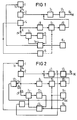
- a low-frequency current I NF of constant amplitude is superimposed on the current I D of the photodiode 6 serving as the receiving diode.
- the resulting change in the bias voltage U, which is at the cathode of the photodiode 6, is measured, rectified with the aid of the rectifier device 9, logarithmic in the logarithmizer 3 and measured with the aid of a linear voltmeter connected to the measuring connection M.
- Fig. 1 shows a circuit arrangement for determining the light output received by the photodiode 6.
- the photodiode 6 is located at the input of the high-frequency amplifier 7, which belongs to an electro-optical receiver.
- the bias voltage U of the photodiode 6 is supplied by the device 1 for bias voltage generation.
- the device 1 belongs to a control device that controls the bias of the photodiode 6 as a function of the light output that the photodiode 6 receives. In this way, the peak value of the high-frequency useful signal current is regulated to a constant value.
- the control device contains the peak value rectifier 13 and the controller 14 connected to the output of the high-frequency amplifier 7.
- the controller 14 is connected with its actual value input to the output of the peak value rectifier 13 and with its setpoint input to the setpoint generator 16.
- the output of the controller 14 is led to the control input 1a of the device 1 for generating the bias voltage.
- the impedance converter 8, the output of which is led to the input of the rectifier arrangement 9, is connected to the cathode of the photodiode 6 carrying the bias voltage.
- the voltage / current converter 10 is connected downstream of the output of the rectifier arrangement 9.
- the outputs of the device 2 for current measurement and the output of the voltage / current converter 10 are routed together to the input 3 of the logarithmizer 3.
- the output M of the circuit arrangement is at the output of the current / voltage converter 17 connected downstream of the logarithmizer 3.
- the low-frequency differential voltage dU to be measured which results from the superimposition of the low-frequency current, is rectified in the rectifier device 9, which is preferably a synchronous rectifier or multiplier.
- the rectifier arrangement 9 is formed by a synchronous rectifier
- an additional input of the rectifier device 9, to which the low-frequency auxiliary signal is fed, is connected to the low-frequency generator 5.
- This embodiment is shown by a dashed line connection of the rectifier device 9 to the low-frequency generator 5.
- the modulation is expediently switched off below an adjustable multiplication factor M, for example for values M ⁇ 1.1.
- M the following are control circuits in particular Regulating circuits to be considered, which are provided in the high-frequency amplifier 7, in particular for gain control.
- the current logarithmizer required for this is used twice in that the bias voltage change dU is converted into a corresponding current with the aid of the voltage / current converter 10 and is fed to the current logarithmizer 3.
- a suitable logarithm which forms the logarithm of its input current, is e.g. B. from the book by J.G. Graeme, G.E. Tobey and L.P, Huelsman “Operational Amplifiers, Design and Applications", Mc GRAW-HILL BOOK COMPANY, 1971, pages 26-263.
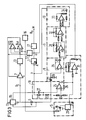
- the circuit arrangement shown in FIG. 2 largely corresponds to that of FIG. 1.
- Deviating from the target voltage supplied by the setpoint generator 16, the output voltage of the low-frequency generator 15 is superimposed.
- the frequency of the low frequency generator 15 is chosen so that it is below the regulator cutoff frequency.
- the resulting change in bias can therefore not be suppressed by the control.
- the low-frequency current I D is superimposed in a simple manner by adding a low-frequency voltage to the nominal value of the control voltage.
- the advantage of such a method is that there is no need to intervene on the high voltage side of the photodiode.
- the comparator 12 is provided. This comparator 12 is together with the impedance converter 8 to the cathode of the Fo Todiode 6 connected. The comparator 12 compares the voltage at the photodiode 6 with a switch-off voltage supplied to the input 12b and its output is connected to the control input 15a of the low-frequency generator 15.
- the device 2 for current measurement is not suitable for values of the multiplication factor M> 1, since the dark current, which is of the order of magnitude of the photocurrent, is multiplied. If the multiplication factor M> 1, the comparator 12 switches the low-frequency generator 15 on.
- the circuit arrangement shown in FIG. 3 largely corresponds to that according to FIG. 2 and shows further details.
- the current I D flows from the device 11 for bias voltage generation via the photodiode 6 and the input resistance of the high-frequency amplifier 7 to ground and from there via a diode located at the input of the logarithmizer 3 back to the connection 11b of the device 11.
- the connection 11b of the device 11 is at a further reference potential.
- the voltage divider consisting of the resistors 21 and 23 lies between the connection of the device 11 carrying the bias voltage and the connection 11b. The current flowing through this voltage divider can therefore not influence the measurement of the current I D by the logarithm 3.
- the shutdown device 18 contains the voltage divider consisting of the resistors 21 and 23 arranged in series with the photodiode 6 and through which the diode current flows.
- the capacitor 22 is connected in parallel to the resistor 21, which is arranged on the side of the voltage divider facing away from the photodiode 6.
- the bias voltage of the photodiode 6 is located at the voltage divider.
- the tap of the voltage divider is routed to the minus input of the operational amplifier 25, the positive input of which is at the tap of the further voltage divider 24, which is connected to a desired voltage.
- the output of the comparator 25, which is supplemented with the aid of the resistor 26 to form a Schmitt trigger, is led to the control input 20a of the timer 20 contained in the low-frequency generator 15. If the bias voltage of the photodiode falls below a predetermined value (M ⁇ 1.1), the timer 20 is stopped and the controller 14a, 14b is not supplied with a low frequency.
- the timer 20 has a control input 20a and can be stopped using a switch-off signal applied to the control input 20a.
- the impedance converter 8 contains a chain circuit comprising the high-pass filter 27, 28 and the operational amplifier 29.
- the operational amplifier 29 is connected to the cathode of the photodiode 6 via the capacitor 27 of the high-pass filter.
- the comparatively high bias voltage at the cathode of the photodiode 6 is therefore kept away from the input of the operational amplifier 29.
- the high-pass filter contains the capacitor 27 in a longitudinal branch and the high-resistance resistor 28 in a subsequent transverse branch.
- the high-pass filter is dimensioned such that the low frequency originating from the low-frequency generator 15 is let through.
- the operational amplifier 29 operated as an emitter follower has a comparatively high input and an input amplifier Output has a comparatively low resistance.
- the impedance converter 8 ensures that the impedance conditions at the photodiode 6 are practically not influenced by the rectifier arrangement 9.
- the rectifier arrangement 9 is connected to the capacitor 30 located at the output of the impedance converter 8.
- the rectifier arrangement 9 contains an arrangement 31 for peak value rectification, which is designed as an active full-wave rectifier.
- the arrangement 32 for the peak value rectification is followed by the arrangement 32 for the screening, which as an active low-pass filter causes a screening of the low frequency.
- the voltage / current converter 10 following the arrangement 32 is realized with the aid of the operational amplifier 33.
- the diode 34 located at the output of the active voltage / current converter 10 causes decoupling and is led to the circuit point a located at the input of the logarithmizer 3, at which the current coming from the device 2 for current measurement and the current coming from the voltage / current converter 10 be added.
- the controller 14 contains two control amplifiers, which have their setpoint inputs + at the common setpoint generator 16 and via the RC series circuit 19 at the output of the timer 20.
- the actual value inputs - the control amplifiers 14a and 14b are located jointly at the output of the peak value rectifier 13.
- the control amplifier 14a serves to regulate the bias of the photodiode 6.
- the control amplifier 14b controls the amplification of the high-frequency amplifier 7.
- the control voltage generated in this case is in addition to the control input of the high-frequency amplifier 7 led to the output of the logarithmizer 3 via the voltage / current converter 37.
- the regulation of the bias voltage of the photodiode 6 and the amplification of the amplifier 7 is carried out in such a way that the bias voltage is initially regulated at low light outputs and the HF amplification of the amplifier 7 when the light output increases (M ⁇ 1.1). In the latter case, the low is frequency generator 15 switched off.
- the output current of the logarithmizer 3 the output current of the voltage / current converter 38 and the output current of the constant current source 35 are added.
- the light output is measured with the help of the switching means 8, 9 and 10.
- the current flowing through the photodiode 6 can be neglected even at the input of the logarithmizer 3.
- the current supplied by the constant current source 35 to the switching point b has the opposite polarity to the output current of the logarithmizer 3, so that a constant amount is subtracted from the output current of the logarithmizer 3. This makes it possible that the input current of the logarithmizer 3 can be selected so that it is significantly larger than the photo current, i. H. that the photo current added at node a remains without influence.
- the light output display can also be used at values smaller than the minimum sensitivity of the system.
- the status "no light” can be displayed.
- the lower current range described is followed by a medium current range in which the measurement is based on the control voltage supplied to the high-frequency amplifier 7.
- This control voltage is practically exclusively effective at the switching point b, since the constant current source 35 and the low-frequency generator 15 are switched off in this measuring range (M ⁇ 1.1).
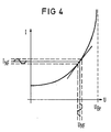
- FIG. 4 shows the typical course of the characteristic curve of an APD.
- the characteristic curve of the APD is subject to relatively large sample variations. Depending on the voltage U Br, the characteristic curve shifts parallel in the direction of the voltage axis. This deviation can be several volts. Since the course of the characteristic is retained and only the position in the direction of the voltage axis is different, the measurement result, which is based on the slope of the characteristic, is advantageously independent of the offset of the characteristic.
Landscapes
- Physics & Mathematics (AREA)
- Electromagnetism (AREA)
- Engineering & Computer Science (AREA)
- Computer Networks & Wireless Communication (AREA)
- Signal Processing (AREA)
- Photometry And Measurement Of Optical Pulse Characteristics (AREA)
- Optical Communication System (AREA)
- Measurement Of Current Or Voltage (AREA)
- Fire-Detection Mechanisms (AREA)
Claims (10)
- Montage pour déterminer la puissance lumineuse reçue par une photodiode (6) d'un récepteur optique, dans lequel la tension de polarisation de la photodiode est réglée au moyen d'un dispositif de régulation (1) en fonction de la puissance lumineuse reçue, le montage comportant un dispositif de modulation, à l'aide duquel un courant à basse fréquence, possédant une amplitude constante, est superposé au courant photoélectrique de la photodiode (6), et à la photodiode (6) est raccordé un dispositif redresseur (9), qui redresse la tension à basse fréquence, qui résulte du courant à basse fréquence superposé et dont la sortie est raccordée à une sortie de mesure (M) pour le raccordement d'un dispositif d'affichage.
- Montage suivant la revendication 1, caractérisé par le fait qu'une unité de mise sous forme logarithmique (3) est prévue entre le dispositif redresseur (9) et la sortie de mesure (M).
- Montage suivant la revendication 1, caractérisé par le fait que le courant photoélectrique de la photodiode (6) est transmis par l'intermédiaire d'un additionneur de courant qui est raccordé à un générateur à basse fréquence.
- Montage suivant la revendication 1 ou 2, caractérisé par le fait que le montage comporte un dispositif de régulation qui maintient constant le courant photoélectrique de la photodiode (6) et qu'à la valeur de consigne, envoyée à l'entrée de la valeur de consigne du dispositif de régulation (14), est additionnée une tension à basse fréquence, dont la fréquence est inférieure à la fréquence limite du circuit de régulation fermé.
- Montage suivant la revendication 1, caractérisé par le fait que la photodiode (6) est formée par une photodiode à avalanche et que le dispositif de modulation fait partie d'un dispositif de régulation servant à régler le facteur multiplicatif respectivement optimum.
- Montage suivant l'une des revendications 1 à 4, caractérisé par le fait que la photodiode (6) est formée par une photodiode à avalanche et qu'il est prévu un dispositif d'interruption (comparateur 12) servant à interrompre la modulation du courant de la diode lorsque le facteur multiplicatif de la photodiode à avalanche tombe au-dessous d'une valeur prédéterminée.
- Montage suivant l'une des revendications 1 à 6, caractérisé par le fait que le dispositif redresseur (9) est formé par un redresseur synchrone, qui est raccordé à la photodiode (6) et au générateur à basse fréquence (5,15).
- Montage suivant l'une des revendications 2 à 7, caractérisé par le fait que pour une gamme moyenne de la puissance lumineuse pouvant être déterminée, il est prévu un dispositif servant à mesurer la grandeur de réglage envoyée à un circuit de réglage du récepteur optique.
- Montage suivant l'une des revendications 1 à 8, caractérisé par le fait qu'en série avec la photodiode (6) est prévu un dispositif de mesure du courant qui envoie un courant injecté à l'unité de mise sous forme logarithmique (3), et qu'un convertisseur tension/courant (10) est disposé entre le dispositif redresseur (9) et l'unité de mise sous forme logarithmique.
- Montage suivant l'une des revendications 1 à 9, caractérisé par le fait qu'un convertisseur d'impédance (8) est disposé entre la photodiode (6) et le dispositif redresseur (9).
Priority Applications (5)
| Application Number | Priority Date | Filing Date | Title |
|---|---|---|---|
| DE3852394T DE3852394D1 (de) | 1988-09-15 | 1988-09-15 | Schaltungsanordnung zur Ermittlung einer empfangenen Lichtleistung. |
| EP88115133A EP0360877B1 (fr) | 1988-09-15 | 1988-09-15 | Circuit pour déterminer la puissance optique d'un signal |
| AT88115133T ATE115343T1 (de) | 1988-09-15 | 1988-09-15 | Schaltungsanordnung zur ermittlung einer empfangenen lichtleistung. |
| JP1237367A JPH02168125A (ja) | 1988-09-15 | 1989-09-14 | 受光された光出力の検出回路装置 |
| US07/407,741 US5004907A (en) | 1988-09-15 | 1989-09-15 | Circuit for determining power of received light having superimposition of low frequency current |
Applications Claiming Priority (1)
| Application Number | Priority Date | Filing Date | Title |
|---|---|---|---|
| EP88115133A EP0360877B1 (fr) | 1988-09-15 | 1988-09-15 | Circuit pour déterminer la puissance optique d'un signal |
Publications (2)
| Publication Number | Publication Date |
|---|---|
| EP0360877A1 EP0360877A1 (fr) | 1990-04-04 |
| EP0360877B1 true EP0360877B1 (fr) | 1994-12-07 |
Family
ID=8199323
Family Applications (1)
| Application Number | Title | Priority Date | Filing Date |
|---|---|---|---|
| EP88115133A Expired - Lifetime EP0360877B1 (fr) | 1988-09-15 | 1988-09-15 | Circuit pour déterminer la puissance optique d'un signal |
Country Status (5)
| Country | Link |
|---|---|
| US (1) | US5004907A (fr) |
| EP (1) | EP0360877B1 (fr) |
| JP (1) | JPH02168125A (fr) |
| AT (1) | ATE115343T1 (fr) |
| DE (1) | DE3852394D1 (fr) |
Families Citing this family (6)
| Publication number | Priority date | Publication date | Assignee | Title |
|---|---|---|---|---|
| US5208796A (en) * | 1991-01-03 | 1993-05-04 | Xerox Corporation | Method and apparatus for transverse image registration on photoreceptive belts |
| FI105064B (fi) * | 1993-11-05 | 2000-05-31 | Nokia Networks Oy | Menetelmä APD-vastaanottimen optisen tulotehon määrittämiseksi |
| US6313459B1 (en) | 2000-05-31 | 2001-11-06 | Nortel Networks Limited | Method for calibrating and operating an uncooled avalanche photodiode optical receiver |
| JP2003158493A (ja) * | 2001-11-21 | 2003-05-30 | Mitsubishi Electric Corp | 光遮断検出装置、光受信器、光送信器及び光遮断検出方法 |
| JP3956923B2 (ja) * | 2003-09-19 | 2007-08-08 | 住友電気工業株式会社 | アバランシェフォトダイオードのバイアス電圧制御回路 |
| US7297922B2 (en) | 2005-09-28 | 2007-11-20 | Intel Corporation | Optical receiver protection circuit |
Family Cites Families (7)
| Publication number | Priority date | Publication date | Assignee | Title |
|---|---|---|---|---|
| US2862109A (en) * | 1954-08-11 | 1958-11-25 | Westinghouse Electric Corp | Phototransistor light detector |
| US4236069A (en) * | 1978-10-16 | 1980-11-25 | Varo, Inc. | Avalanche photodiode gain control system |
| FR2475826A1 (fr) * | 1980-02-12 | 1981-08-14 | Lignes Telegraph Telephon | Dispositif de declenchement d'alarme pour une insuffisance du niveau de transmission, pour module recepteur d'un systeme de transmission sur fibre optique |
| FR2510267B1 (fr) * | 1981-07-21 | 1986-05-02 | Lignes Telegraph Telephon | Dispositif de mesure d'attenuation d'une liaison par fibre optique |
| US4805236A (en) * | 1986-12-15 | 1989-02-14 | Oy Nokia Ab | Method and arrangement for increasing the dynamic range at an input stage of an optical receiver |
| DE3870493D1 (de) * | 1987-03-17 | 1992-06-04 | Siemens Ag | Regelung des multiplikationsfaktors von lawinenphotodioden in optischen empfaengern. |
| EP0313914B1 (fr) * | 1987-10-26 | 1993-03-03 | Siemens Aktiengesellschaft | Circuit comportant un préamplificateur connecté à un transducteur opto-électrique |
-
1988
- 1988-09-15 AT AT88115133T patent/ATE115343T1/de not_active IP Right Cessation
- 1988-09-15 EP EP88115133A patent/EP0360877B1/fr not_active Expired - Lifetime
- 1988-09-15 DE DE3852394T patent/DE3852394D1/de not_active Expired - Fee Related
-
1989
- 1989-09-14 JP JP1237367A patent/JPH02168125A/ja active Pending
- 1989-09-15 US US07/407,741 patent/US5004907A/en not_active Expired - Fee Related
Also Published As
| Publication number | Publication date |
|---|---|
| EP0360877A1 (fr) | 1990-04-04 |
| DE3852394D1 (de) | 1995-01-19 |
| JPH02168125A (ja) | 1990-06-28 |
| US5004907A (en) | 1991-04-02 |
| ATE115343T1 (de) | 1994-12-15 |
Similar Documents
| Publication | Publication Date | Title |
|---|---|---|
| EP0009220B1 (fr) | Système pour la transmission de signaux par une liaison optique | |
| DE69718004T2 (de) | System mit einem optischen verstärker | |
| DE19882819B4 (de) | Optische Empfangsvorrichtung | |
| EP0360877B1 (fr) | Circuit pour déterminer la puissance optique d'un signal | |
| DE2535695B2 (de) | Verstärkerschaltung mit selbsttätiger Regelung der Verstärkung | |
| DE69205924T2 (de) | Kontinuierlich abstimmbarer Laseroszillator. | |
| DE69333695T2 (de) | Schaltung zur Leistungsberechnung | |
| EP0227908A1 (fr) | Dispositif pour la mesure de tension en prenant des échantillons | |
| DE69221231T2 (de) | Vorrichtung zur Leistungssteuerung | |
| DE4411063A1 (de) | Verfahren zur Bestimmung der Dispersionsnullstelle eines Lichtwellenleiters | |
| DE3638316C2 (fr) | ||
| DE3605488C2 (de) | Detektorvorverstärker | |
| DE3147171C2 (fr) | ||
| DE2311676A1 (de) | Weg-spannungswandler | |
| DE2631454C3 (de) | Flammenmelder | |
| DE2727212C3 (de) | Signalstärkemesser-Treiberschaltung in einem Empfänger | |
| DE60002588T2 (de) | Photometer | |
| EP0282801B1 (fr) | Réglage du gain de photodiodes à avalanche dans des récepteurs optiques | |
| DE69528320T2 (de) | Optische Frequenzmischanordnung | |
| DE2933840C2 (de) | Schaltungsanordnung zur Überprüfung und Steuerung der Koeffizienten eines analogen adaptiven Entzerrers | |
| DE1547136B2 (fr) | ||
| DE2743951C2 (de) | Optoelektronischer Weg-Spannungswandler zur Abstandsmessung zweier Objekte | |
| DE1516253C3 (de) | Verfahren und Schaltungsanordnung zur Messung der Phasenverzerrungen eines elektrischen Vierpols, insbesondere Übertragungssystems | |
| DE69225833T2 (de) | Optischer Sender | |
| DE2607206A1 (de) | Fotostromverstaerker |
Legal Events
| Date | Code | Title | Description |
|---|---|---|---|
| PUAI | Public reference made under article 153(3) epc to a published international application that has entered the european phase |
Free format text: ORIGINAL CODE: 0009012 |
|
| AK | Designated contracting states |
Kind code of ref document: A1 Designated state(s): AT BE CH DE ES FR GB GR IT LI NL SE |
|
| 17P | Request for examination filed |
Effective date: 19900919 |
|
| 17Q | First examination report despatched |
Effective date: 19930820 |
|
| GRAA | (expected) grant |
Free format text: ORIGINAL CODE: 0009210 |
|
| AK | Designated contracting states |
Kind code of ref document: B1 Designated state(s): AT BE CH DE FR GB IT LI NL SE |
|
| PG25 | Lapsed in a contracting state [announced via postgrant information from national office to epo] |
Ref country code: IT Free format text: LAPSE BECAUSE OF FAILURE TO SUBMIT A TRANSLATION OF THE DESCRIPTION OR TO PAY THE FEE WITHIN THE PRE;WARNING: LAPSES OF ITALIAN PATENTS WITH EFFECTIVE DATE BEFORE 2007 MAY HAVE OCCURRED AT ANY TIME BEFORE 2007. THE CORRECT EFFECTIVE DATE MAY BE DIFFERENT FROM THE ONE RECORDED.SCRIBED TIME-LIMIT Effective date: 19941207 Ref country code: GB Effective date: 19941207 Ref country code: BE Effective date: 19941207 Ref country code: FR Effective date: 19941207 Ref country code: NL Effective date: 19941207 |
|
| REF | Corresponds to: |
Ref document number: 115343 Country of ref document: AT Date of ref document: 19941215 Kind code of ref document: T |
|
| REF | Corresponds to: |
Ref document number: 3852394 Country of ref document: DE Date of ref document: 19950119 |
|
| PG25 | Lapsed in a contracting state [announced via postgrant information from national office to epo] |
Ref country code: SE Effective date: 19950307 |
|
| EN | Fr: translation not filed | ||
| NLV1 | Nl: lapsed or annulled due to failure to fulfill the requirements of art. 29p and 29m of the patents act | ||
| GBV | Gb: ep patent (uk) treated as always having been void in accordance with gb section 77(7)/1977 [no translation filed] |
Effective date: 19941207 |
|
| PG25 | Lapsed in a contracting state [announced via postgrant information from national office to epo] |
Ref country code: AT Effective date: 19950915 |
|
| PG25 | Lapsed in a contracting state [announced via postgrant information from national office to epo] |
Ref country code: CH Effective date: 19950930 Ref country code: LI Effective date: 19950930 |
|
| PLBE | No opposition filed within time limit |
Free format text: ORIGINAL CODE: 0009261 |
|
| STAA | Information on the status of an ep patent application or granted ep patent |
Free format text: STATUS: NO OPPOSITION FILED WITHIN TIME LIMIT |
|
| PGFP | Annual fee paid to national office [announced via postgrant information from national office to epo] |
Ref country code: DE Payment date: 19951116 Year of fee payment: 8 |
|
| 26N | No opposition filed | ||
| REG | Reference to a national code |
Ref country code: CH Ref legal event code: PL |
|
| PG25 | Lapsed in a contracting state [announced via postgrant information from national office to epo] |
Ref country code: DE Effective date: 19970603 |