EP0361206A1 - Article revêtu d'un film céramique - Google Patents
Article revêtu d'un film céramique Download PDFInfo
- Publication number
- EP0361206A1 EP0361206A1 EP89116885A EP89116885A EP0361206A1 EP 0361206 A1 EP0361206 A1 EP 0361206A1 EP 89116885 A EP89116885 A EP 89116885A EP 89116885 A EP89116885 A EP 89116885A EP 0361206 A1 EP0361206 A1 EP 0361206A1
- Authority
- EP
- European Patent Office
- Prior art keywords
- article
- film
- base member
- carbon
- carbonaceous film
- Prior art date
- Legal status (The legal status is an assumption and is not a legal conclusion. Google has not performed a legal analysis and makes no representation as to the accuracy of the status listed.)
- Granted
Links
- 239000000919 ceramic Substances 0.000 title claims description 10
- OKTJSMMVPCPJKN-UHFFFAOYSA-N Carbon Chemical compound [C] OKTJSMMVPCPJKN-UHFFFAOYSA-N 0.000 claims abstract description 43
- 229910052799 carbon Inorganic materials 0.000 claims abstract description 43
- 239000000463 material Substances 0.000 claims abstract description 19
- 229910052736 halogen Inorganic materials 0.000 claims abstract description 11
- 150000002367 halogens Chemical class 0.000 claims abstract description 11
- 239000004020 conductor Substances 0.000 claims abstract description 6
- 238000010422 painting Methods 0.000 claims abstract 4
- 239000000126 substance Substances 0.000 claims abstract 3
- 239000011737 fluorine Substances 0.000 claims description 14
- 229910052731 fluorine Inorganic materials 0.000 claims description 14
- 238000000034 method Methods 0.000 claims description 12
- 229910052581 Si3N4 Inorganic materials 0.000 claims description 3
- 239000005871 repellent Substances 0.000 claims description 3
- 230000005684 electric field Effects 0.000 claims description 2
- 238000004519 manufacturing process Methods 0.000 claims description 2
- 125000001153 fluoro group Chemical group F* 0.000 claims 1
- 239000010408 film Substances 0.000 description 66
- 239000007789 gas Substances 0.000 description 31
- 239000000758 substrate Substances 0.000 description 25
- YCKRFDGAMUMZLT-UHFFFAOYSA-N Fluorine atom Chemical compound [F] YCKRFDGAMUMZLT-UHFFFAOYSA-N 0.000 description 13
- 238000006243 chemical reaction Methods 0.000 description 13
- IJGRMHOSHXDMSA-UHFFFAOYSA-N Atomic nitrogen Chemical compound N#N IJGRMHOSHXDMSA-UHFFFAOYSA-N 0.000 description 12
- 238000000576 coating method Methods 0.000 description 10
- 239000000428 dust Substances 0.000 description 10
- 239000011248 coating agent Substances 0.000 description 8
- 238000005268 plasma chemical vapour deposition Methods 0.000 description 8
- 230000001681 protective effect Effects 0.000 description 7
- VGGSQFUCUMXWEO-UHFFFAOYSA-N Ethene Chemical compound C=C VGGSQFUCUMXWEO-UHFFFAOYSA-N 0.000 description 6
- 239000005977 Ethylene Substances 0.000 description 6
- WMIYKQLTONQJES-UHFFFAOYSA-N hexafluoroethane Chemical compound FC(F)(F)C(F)(F)F WMIYKQLTONQJES-UHFFFAOYSA-N 0.000 description 6
- 239000001257 hydrogen Substances 0.000 description 6
- 229910052739 hydrogen Inorganic materials 0.000 description 6
- 229910052757 nitrogen Inorganic materials 0.000 description 6
- 230000005611 electricity Effects 0.000 description 5
- 239000000203 mixture Substances 0.000 description 5
- GVGCUCJTUSOZKP-UHFFFAOYSA-N nitrogen trifluoride Chemical compound FN(F)F GVGCUCJTUSOZKP-UHFFFAOYSA-N 0.000 description 5
- 239000011368 organic material Substances 0.000 description 5
- 239000003973 paint Substances 0.000 description 5
- 230000003068 static effect Effects 0.000 description 5
- TXEYQDLBPFQVAA-UHFFFAOYSA-N tetrafluoromethane Chemical compound FC(F)(F)F TXEYQDLBPFQVAA-UHFFFAOYSA-N 0.000 description 5
- 239000000654 additive Substances 0.000 description 4
- 150000002430 hydrocarbons Chemical class 0.000 description 4
- QYSGYZVSCZSLHT-UHFFFAOYSA-N octafluoropropane Chemical compound FC(F)(F)C(F)(F)C(F)(F)F QYSGYZVSCZSLHT-UHFFFAOYSA-N 0.000 description 4
- 229920005989 resin Polymers 0.000 description 4
- 239000011347 resin Substances 0.000 description 4
- 238000004544 sputter deposition Methods 0.000 description 4
- 239000010409 thin film Substances 0.000 description 4
- 239000004215 Carbon black (E152) Substances 0.000 description 3
- UFHFLCQGNIYNRP-UHFFFAOYSA-N Hydrogen Chemical compound [H][H] UFHFLCQGNIYNRP-UHFFFAOYSA-N 0.000 description 3
- 238000005299 abrasion Methods 0.000 description 3
- 230000015572 biosynthetic process Effects 0.000 description 3
- 230000000694 effects Effects 0.000 description 3
- 229930195733 hydrocarbon Natural products 0.000 description 3
- 150000002431 hydrogen Chemical class 0.000 description 3
- 239000011253 protective coating Substances 0.000 description 3
- XKRFYHLGVUSROY-UHFFFAOYSA-N Argon Chemical compound [Ar] XKRFYHLGVUSROY-UHFFFAOYSA-N 0.000 description 2
- XOJVVFBFDXDTEG-UHFFFAOYSA-N Norphytane Natural products CC(C)CCCC(C)CCCC(C)CCCC(C)C XOJVVFBFDXDTEG-UHFFFAOYSA-N 0.000 description 2
- 229910007264 Si2H6 Inorganic materials 0.000 description 2
- VYPSYNLAJGMNEJ-UHFFFAOYSA-N Silicium dioxide Chemical compound O=[Si]=O VYPSYNLAJGMNEJ-UHFFFAOYSA-N 0.000 description 2
- MCMNRKCIXSYSNV-UHFFFAOYSA-N Zirconium dioxide Chemical compound O=[Zr]=O MCMNRKCIXSYSNV-UHFFFAOYSA-N 0.000 description 2
- 238000009825 accumulation Methods 0.000 description 2
- -1 acryl Chemical group 0.000 description 2
- 230000000996 additive effect Effects 0.000 description 2
- 229920000180 alkyd Polymers 0.000 description 2
- 239000012159 carrier gas Substances 0.000 description 2
- 239000002131 composite material Substances 0.000 description 2
- 238000000354 decomposition reaction Methods 0.000 description 2
- RWRIWBAIICGTTQ-UHFFFAOYSA-N difluoromethane Chemical compound FCF RWRIWBAIICGTTQ-UHFFFAOYSA-N 0.000 description 2
- PZPGRFITIJYNEJ-UHFFFAOYSA-N disilane Chemical compound [SiH3][SiH3] PZPGRFITIJYNEJ-UHFFFAOYSA-N 0.000 description 2
- 239000002075 main ingredient Substances 0.000 description 2
- VNWKTOKETHGBQD-UHFFFAOYSA-N methane Chemical compound C VNWKTOKETHGBQD-UHFFFAOYSA-N 0.000 description 2
- 230000003287 optical effect Effects 0.000 description 2
- 229920006254 polymer film Polymers 0.000 description 2
- 239000004925 Acrylic resin Substances 0.000 description 1
- 229920000178 Acrylic resin Polymers 0.000 description 1
- 229910020211 SiOxHy Inorganic materials 0.000 description 1
- 229910020286 SiOxNy Inorganic materials 0.000 description 1
- 229910000831 Steel Inorganic materials 0.000 description 1
- XAGFODPZIPBFFR-UHFFFAOYSA-N aluminium Chemical compound [Al] XAGFODPZIPBFFR-UHFFFAOYSA-N 0.000 description 1
- 229920003180 amino resin Polymers 0.000 description 1
- 229910052786 argon Inorganic materials 0.000 description 1
- QVGXLLKOCUKJST-UHFFFAOYSA-N atomic oxygen Chemical compound [O] QVGXLLKOCUKJST-UHFFFAOYSA-N 0.000 description 1
- 239000003990 capacitor Substances 0.000 description 1
- 239000003575 carbonaceous material Substances 0.000 description 1
- 230000015556 catabolic process Effects 0.000 description 1
- 229910052681 coesite Inorganic materials 0.000 description 1
- 229910052906 cristobalite Inorganic materials 0.000 description 1
- 238000006115 defluorination reaction Methods 0.000 description 1
- 238000000151 deposition Methods 0.000 description 1
- 230000008021 deposition Effects 0.000 description 1
- 238000009826 distribution Methods 0.000 description 1
- 238000005516 engineering process Methods 0.000 description 1
- 238000005530 etching Methods 0.000 description 1
- IPZIVCLZBFDXTA-UHFFFAOYSA-N ethyl n-prop-2-enoylcarbamate Chemical compound CCOC(=O)NC(=O)C=C IPZIVCLZBFDXTA-UHFFFAOYSA-N 0.000 description 1
- JEIPFZHSYJVQDO-UHFFFAOYSA-N iron(III) oxide Inorganic materials O=[Fe]O[Fe]=O JEIPFZHSYJVQDO-UHFFFAOYSA-N 0.000 description 1
- 230000001788 irregular Effects 0.000 description 1
- 239000004922 lacquer Substances 0.000 description 1
- 238000011068 loading method Methods 0.000 description 1
- 229910003465 moissanite Inorganic materials 0.000 description 1
- DHQIYHHEPUYAAX-UHFFFAOYSA-N n-(4,6-diamino-1,3,5-triazin-2-yl)prop-2-enamide Chemical compound NC1=NC(N)=NC(NC(=O)C=C)=N1 DHQIYHHEPUYAAX-UHFFFAOYSA-N 0.000 description 1
- 239000001301 oxygen Substances 0.000 description 1
- 229910052760 oxygen Inorganic materials 0.000 description 1
- 229920001225 polyester resin Polymers 0.000 description 1
- 239000004645 polyester resin Substances 0.000 description 1
- 229920000642 polymer Polymers 0.000 description 1
- 238000002360 preparation method Methods 0.000 description 1
- 230000002265 prevention Effects 0.000 description 1
- 230000003449 preventive effect Effects 0.000 description 1
- 230000001105 regulatory effect Effects 0.000 description 1
- 229910010271 silicon carbide Inorganic materials 0.000 description 1
- 239000000377 silicon dioxide Substances 0.000 description 1
- 235000012239 silicon dioxide Nutrition 0.000 description 1
- 239000010959 steel Substances 0.000 description 1
- 229910052682 stishovite Inorganic materials 0.000 description 1
- 229910052905 tridymite Inorganic materials 0.000 description 1
- 229920006337 unsaturated polyester resin Polymers 0.000 description 1
Images

Classifications
-
- B—PERFORMING OPERATIONS; TRANSPORTING
- B05—SPRAYING OR ATOMISING IN GENERAL; APPLYING FLUENT MATERIALS TO SURFACES, IN GENERAL
- B05D—PROCESSES FOR APPLYING FLUENT MATERIALS TO SURFACES, IN GENERAL
- B05D3/00—Pretreatment of surfaces to which liquids or other fluent materials are to be applied; After-treatment of applied coatings, e.g. intermediate treating of an applied coating preparatory to subsequent applications of liquids or other fluent materials
- B05D3/10—Pretreatment of surfaces to which liquids or other fluent materials are to be applied; After-treatment of applied coatings, e.g. intermediate treating of an applied coating preparatory to subsequent applications of liquids or other fluent materials by other chemical means
-
- C—CHEMISTRY; METALLURGY
- C23—COATING METALLIC MATERIAL; COATING MATERIAL WITH METALLIC MATERIAL; CHEMICAL SURFACE TREATMENT; DIFFUSION TREATMENT OF METALLIC MATERIAL; COATING BY VACUUM EVAPORATION, BY SPUTTERING, BY ION IMPLANTATION OR BY CHEMICAL VAPOUR DEPOSITION, IN GENERAL; INHIBITING CORROSION OF METALLIC MATERIAL OR INCRUSTATION IN GENERAL
- C23C—COATING METALLIC MATERIAL; COATING MATERIAL WITH METALLIC MATERIAL; SURFACE TREATMENT OF METALLIC MATERIAL BY DIFFUSION INTO THE SURFACE, BY CHEMICAL CONVERSION OR SUBSTITUTION; COATING BY VACUUM EVAPORATION, BY SPUTTERING, BY ION IMPLANTATION OR BY CHEMICAL VAPOUR DEPOSITION, IN GENERAL
- C23C16/00—Chemical coating by decomposition of gaseous compounds, without leaving reaction products of surface material in the coating, i.e. chemical vapour deposition [CVD] processes
- C23C16/22—Chemical coating by decomposition of gaseous compounds, without leaving reaction products of surface material in the coating, i.e. chemical vapour deposition [CVD] processes characterised by the deposition of inorganic material, other than metallic material
- C23C16/26—Deposition of carbon only
-
- C—CHEMISTRY; METALLURGY
- C23—COATING METALLIC MATERIAL; COATING MATERIAL WITH METALLIC MATERIAL; CHEMICAL SURFACE TREATMENT; DIFFUSION TREATMENT OF METALLIC MATERIAL; COATING BY VACUUM EVAPORATION, BY SPUTTERING, BY ION IMPLANTATION OR BY CHEMICAL VAPOUR DEPOSITION, IN GENERAL; INHIBITING CORROSION OF METALLIC MATERIAL OR INCRUSTATION IN GENERAL
- C23C—COATING METALLIC MATERIAL; COATING MATERIAL WITH METALLIC MATERIAL; SURFACE TREATMENT OF METALLIC MATERIAL BY DIFFUSION INTO THE SURFACE, BY CHEMICAL CONVERSION OR SUBSTITUTION; COATING BY VACUUM EVAPORATION, BY SPUTTERING, BY ION IMPLANTATION OR BY CHEMICAL VAPOUR DEPOSITION, IN GENERAL
- C23C16/00—Chemical coating by decomposition of gaseous compounds, without leaving reaction products of surface material in the coating, i.e. chemical vapour deposition [CVD] processes
- C23C16/44—Chemical coating by decomposition of gaseous compounds, without leaving reaction products of surface material in the coating, i.e. chemical vapour deposition [CVD] processes characterised by the method of coating
- C23C16/50—Chemical coating by decomposition of gaseous compounds, without leaving reaction products of surface material in the coating, i.e. chemical vapour deposition [CVD] processes characterised by the method of coating using electric discharges
- C23C16/505—Chemical coating by decomposition of gaseous compounds, without leaving reaction products of surface material in the coating, i.e. chemical vapour deposition [CVD] processes characterised by the method of coating using electric discharges using radio frequency discharges
- C23C16/509—Chemical coating by decomposition of gaseous compounds, without leaving reaction products of surface material in the coating, i.e. chemical vapour deposition [CVD] processes characterised by the method of coating using electric discharges using radio frequency discharges using internal electrodes
Definitions
- the present invention relates to an article coated with a ceramic film such as a carbonaceous film, specifically to a ceramic protective film e.g. made of carbon, or of a material in which carbon is the main component, to be coated on a painted surface of an article e.g. a bumper or other part of a transportation means such as an automobile, ship, aircraft, and the like.
- a ceramic film such as a carbonaceous film
- a ceramic protective film e.g. made of carbon, or of a material in which carbon is the main component
- an article e.g. a bumper or other part of a transportation means such as an automobile. ship, aircraft, and the like has a surface painted with an organic paint, which can be exposed to wind and rain as well as being a wind-ward leading edge, so that resistance to wear, adherence of dust, and the creation of static electricity in the painted surface must be prevented.
- the plasma CVD method is an industrially effective method of forming a level film on a substrate with a flat surface in the article as mentioned above.
- the sputtering effect using the plasma CVD method is also known as a film forming method.
- a film cannot be formed on a chassis or part, especially on a base member which has an irregular surface, such as on an automobile or motorcycle or the like, or on a large base member such as the chassis of an automobile or the like. For this reason, there is a demand for a method for forming a film in one operation over a large area.
- An object of the present invention is to provide, with due consideration to the drawbacks of such conventional devices, a protective ceramic film.
- Another object of the present invention is to provide a carbonaceous film as the protective film made of carbon, or of a material in which carbon is the main component with tight adherence to an organic material.
- Another object of the present invention is to provide a protective film for preventing wear, as this type of thin film, made of carbon, or of a material in which carbon is the main component, which is translucent in the visible region, and has adequate hardness.
- Another object of the present invention is to provide a protective film which adheres closely to an organic material, can prevent the creation of static electricity, and has a smooth surface, thereby preventing the adherence of dust.
- the present invention proposes the provision of a plasma polymer film of carbon, or of a material in which carbon is the main component, containing a halogen element such as fluorine, as a protective coating on a surface of a bumper or some other part of a chassis for an automobile, ship, aircraft, or the like, which is exposed to wind and rain as well as being a wind-ward leading edge after the surface is painted with an organic coating material.
- a plasma polymer film of carbon or of a material in which carbon is the main component, containing a halogen element such as fluorine, as a protective coating on a surface of a bumper or some other part of a chassis for an automobile, ship, aircraft, or the like, which is exposed to wind and rain as well as being a wind-ward leading edge after the surface is painted with an organic coating material.
- This film has water-shedding or water-repellent capabilities, and prevents the accumulation of dust, while also prevention the development of static electricity which forms easily on a wind-ward leading edge, and preventing the adherence of dust, and abrasion of the painted surfaces from dust thereby preventing the surface from becoming dull, so that the painted surfaces are always maintained in pristine condition.
- the carbonaceous film which has an electrically inherent resistance which has an electrically inherent resistance of 1 x 10⁷ to 5 x 101 ⁇ cm, as a protective coating, on a surface of a bumper or some other part of a chassis for an automobile, ship, aircraft, or the like, which is exposed to wind and rain as well as being a wind-ward leading edge after the surface is painted with an organic coating material.
- This film prevents the accumulation of dust, while also preventing the development of static electricity which forms easily on a wind-ward leading edge, and preventing the adherence of dust, and abrasion of the painted surfaces from dust thereby preventing the surface from becoming dull, so that the painted surfaces are always maintained in pristine condition.
- Another object of the present invention is to provide a method of forming a carbonaceous film of carbon or of a material in which carbon is the main component by the plasma CVD method on a chassis or part.
- Another object of the present invention is to provide a method for forming a carbonaceous film in a single step over a large area, such as the chassis of an automobile or the like.
- a pair of electrodes used for the plasma polymer, specifically for plasma CVD are positioned at each end of the reaction chamber with a space therebetween.
- an AC bias is required with a DC bias overlaid.
- a first alternate voltage is impressed between the two electrodes to convert the reactive gases to plasma.
- High frequency voltages at a phase difference of 180 or 0 degrees are applied with respect to ground from individual high frequency power sources on the respective electrodes, and alternate voltages which are mutually symmetrical or the same phase are applied.
- an essentially matched alternate voltage is applied inside a frame structure, and creates a high frequency plasma.
- the other ends of the high frequency power sources are also grounded, and an additional second alternate voltage is applied via a capacitor to create a DC autobias between these ends and the substrate or substrate holder with a film-forming surface.
- the substrate or the holder for the substrate is used as a third electrode, and by applying an AC bias to the substrate in accordance with the second alternate voltage a thin film is formed using the sputtering effect.
- the first alternate voltage is at a frequency in the range of 1 to 50 MHz, at which a plasma glow discharge is easily produced
- the second alternate voltage is at a frequency in the range of 10 Hz to 500 KHz, at which kinetic energy is easily applied to the reactive gases.
- a negative DC autobias in overlaid and applied to the substrate holder.
- One example of the forming of the thin film is as follows. First, a carbon fluoride gas from carbon fluorides such as C2F6, C3F8, CF4, CH2F2, and the like is introduced. Next, a mixture of this gas and hydrogen is converted to a plasma state, or a mixture of these gases and C2H4 and a hydrocarbon compound is converted to a plasma state, whereby defluorination followed by decomposition is caused by activated hydrogen, so that diamond-like C-C bonds with SP3 orbits are created, whereby a film with diamond-like characteristics, of which the main component is carbon (the secondary components are mainly hydrogen, fluorine, and nitrogen), containing fluorine or a halogen element, is formed.
- the main component is carbon
- This film has a specific resistance (inherent resistance) of 1 x 10⁷ to 5 x 10 13 ⁇ cm, and preferably 1 x 10⁸ to 5 x 10 ⁇ cm, and is translucent in the visible range with an optical band width (Eg) of 1.0 eV or greater, and preferably 1.5 to 5.5 eV.
- Eg optical band width
- Another example of the forming of the thin film is as follows. First, a gas selected from the group of hydrocarbon gas such as ethylene (C2H4), a mixture gas of the hydrocarbon gas and nitrogen fluoride, and a carbon fluoride gas such as C2F6, C3F8, CF4, CH2F2, and the like is introduced for decomposition, so that diamond-like C-C bonds with SP3 orbits are created, whereby a film with diamond-like characteristics, of carbon, or of which the main component is carbon (the secondary components are mainly hydrogen, fluorine, and nitrogen), is formed.
- a gas selected from the group of hydrocarbon gas such as ethylene (C2H4)
- a mixture gas of the hydrocarbon gas and nitrogen fluoride such as C2F6, C3F8, CF4, CH2F2, and the like is introduced for decomposition, so that diamond-like C-C bonds with SP3 orbits are created, whereby a film with diamond-like characteristics, of carbon, or of which the main component is carbon (the secondary components are
- This film has a specific resistance inherent resistance) of 1 x 10⁷ to 5 x 10¹³ ⁇ cm, and preferably 1 x 10⁸ to 5 x 10¹¹ ⁇ cm, and is translucent in the visible range with an optical band width (Eg) of 1.0 eV or greater, and preferably 1.5 to 5.5 eV.
- Eg optical band width
- the painted surface used in the present invention can be a polyester resin, an alkyd resin, an oil-free alkyd resin, an unsaturated polyester resin, an acryl resin, or an amino resin.
- a painted surface using an organic melt type of paint such as acryl lacquer, acryl melamine or block acryl urethane is used.
- a halogen element such as fluorine
- nitrogen are simultaneously added to a carbonaceous gas in plasma CVD.
- a single-layered film or a multilayered composite film may be formed wherein the presence of additives is controlled, so that the carbon content or additive content is change with a uniform gradient concentration in the direction of the thickness provided.
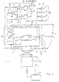
- this drawing gives an outline of a plasma CVD device for implementing a method for forming a thin carbonaceous film on a substrate having a conductor or a conducting surface therein for an automobile chassis or the like.
- CVD device is separated from a preparation chamber 7′ for loading and unloading by a gate valve 9.
- a carrier gas such as argon is introduced through line 31; a reactive gas which is a hydrocarbon gas such as, for example, methane, ethylene, through line 32: an additive gas such as nitrogen fluoride through line 33; a gas for etching the reaction vessel, such as oxygen through line 34.
- gases flow through a nozzle 25 into the reaction system 50 via a valve 28 and a flow meter 29.
- a diamond-like carbonaceous film of 500 to 5000 ⁇ is formed with carbon and fluorine added therein (which is referred to as DLC).
- DLC diamond-like carbonaceous film of 500 to 5000 ⁇ is formed with carbon and fluorine added therein (which is referred to as DLC).
- DLC diamond-like carbonaceous film of 500 to 5000 ⁇ is formed with carbon and fluorine added therein (which is referred to as DLC).
- DLC diamond-like carbonaceous film of
- a film with these same components may be formed by the introduction of C2F6, C3F8 through line 32, and C2H2, or H2 through line 33.
- a film with these same components may be formed by the introduction of C2F6, C3F8 through line 32, and NH3 through line 33.
- a reaction system 50 is provided with a frame structure 2 (observed to have a quadrilateral frame structure when viewed from the electrode).
- a pair of hoods 8, 8′ are provided to cover the open top and bottom sections.
- a pair of first and second identically shaped electrodes 3, 3′ positioned on the hoods 8, 8′ are constructed of aluminum metal mesh. The reactive gases are released in the downward direction from a nozzle 25.
- a substrate 1 which is the chassis, bumper, or other parts of the automobile has a base member and a painted surface as a film-forming surface 1′ thereon.
- the base member forms a third electrode, while the painted surface on the base member is an insulated material for DC currents, but when the second alternate voltage is added here so that a bias is applied it is essentially regarded as a conducting body with respect to AC current.
- the film-forming surface 1′ that is the painted surface of the substrate 1 is positioned and maintained in a plasma created by the pair of electrodes 70(3, 3′).
- the substrate 1 has a film-forming surface 1′ which is a painted organic surface.
- An alternate voltage of 10 Hz to 500 KHz is applied, in the form that the second alternate voltage and a negative DC bias are applied simultaneously.
- a glow discharge of reactive gases which are converted to plasma by a first, high frequency alternate voltage is dispersed uniformly throughout the reaction area 60, and the plasma is surrounded by the frame structure 2 and the hoods 8, 8′, so that the gases in the plasma state are not released in an outer area 6 and the gases do not adhere to the inner walls of the reaction vessel 7.
- the electric potential of the plasma is homogeneous in the reaction area.
- the first alternate voltage has a high frequency of 1 to 100 MHz, for example, 13.56 MHz and is led from a pair of electrodes 15-1, 15-2 to a pair of matching transformers 16-1, 16-2.
- the phases of these matching transformers are adjusted by a phase adjuster. They can be out of phase by 180 or 0 degrees.
- An end 4 and other end 4′ of the transformers, which have a symmetrical or the same phase output, are respectively connected to a pair of electrodes comprising a first electrode 3 and a second electrode 3′.
- a midpoint 5 of the output side of the transformers is maintained in the grounded state, and a second alternate voltage 17 of 10 Hz to 500 KHz, for example, 50 KHz, is applied.
- the output from the midpoint 5 is connected to the third electrode of the substrate 1 or the holder 2 to which the substrate 1 is electrically connected.
- the plasma 60 is created in such a reaction space.
- Unnecessary or unused gases are discharged through a discharge gas system 20 comprising a pressure regulating valve 21, a turbomolecular pump 22, and a rotary pump 23.
- These reactive gases have a pressure of 0.001 to 1.0 torr, for example, 0.05 torr in the reaction space 60, and the frame structure 29 is used as an organic-painted surface for the automobile chassis, motorcycle bumper, or the like.
- the first high frequency voltage of 5 to 50kW (0.3 to 3 W/cm2 per unit area), for example 1kW (0.6 W/cm2 per unit area) is applied at a frequency of 13.56 MHZ.
- a negative autobias voltage of -200 to -600 V (for example, the output of 5 KW) is applied on the film-forming surface.
- the reactive gases accelerated by the negative autobias voltage form a film on the substrate while effecting sputtering, and thus can form a densified film.
- the height of that quadrilateral shaped (rectangular parallelepiped) frame structure may be 2 to 10m, as required by the design.
- the first alternate voltage can be applied between the front and the rear, not between the top and the bottom as shown in the drawing.
- the reactive gases is, for example. a mixture of gases of C2F6 and C2H4.
- the ratio of C2F6 to C2H4 is 1/4 to 4/1, typically 1/1. By varying the ratio, it is possible to control the transmissivity and the specific resistance.
- the temperature of the substrate is maintained at 150°C or less, and typically at room temperature.
- the film is formed on such a film-forming surface and has a specific resistance of 1 x 10⁷ to 5 x 10¹³ ⁇ cm. It can be densely formed on an organic resin.
- a carbonaceous film of carbon, or of a material in which carbon is the main component, to which fluorine is added, with an amorphous structure or a crystalline structure translucent to visible light, is formed at 0.1 to 8 ⁇ m, for example 0.5 ⁇ m (at flat sections), and 1 to 3 ⁇ m ( at projecting sections).
- the film forming velocity is 100 to 1000 ⁇ per minute.
- a carbonaceous film of carbon, or of a material in which carbon is the main component can be formed, in particular one containing 30 atomic% of a halogen element such as fluorine, and also, 0.3 to 10 atomic% of nitrogen mixed in. It is also possible to provide a first layer of carbon to a thickness of 100 to 2000 ⁇ on an organic painted surface, using ethylene only, then, on top of this, a carbonaceous film, to which is added a halogen element such as fluorine, can also be formed.
- This embodiment is an example of the formation of a carbonaceous film, of which carbon is the main component, on an automobile chassis and its principal parts by means of the device used in Embodiment 1, as shown in FIG. 1(A) to FIG. 1(C).
- FIG. 1(A) an automobile chassis in shown in cross-section.
- FIG. 1(B) and FIG. 1(C) show an enlarged drawing of its principal parts.
- the automobile chassis has a base member 42 of steel.
- the base member 42 is subjected to a rust preventive treatment to form an anticorrosive layer 43.
- An organic paint 44 is then applied to this surface on the request of the customer.
- a colored acrylic resin can be provided.
- an abrasion resistant protective carbonaceous film 45 of carbon, or of a material in which carbon is the main component is provided to a thickness of 0.1 to 8 ⁇ m.
- its specific resistance is kept in the range of 1 x 10⁷ to 5 x 10¹³ ⁇ cm and preferably in the range of 1 x 10⁹ to 1 x 10¹¹ ⁇ cm, so that the formation of static electricity or the adherence of dirt can be prevented.
- FIG. 1(C) a projecting section of the chassis or the like is shown. Because a bias electrical field collects here in the plasma CVD and the like, the velocity of the film forming process is increased, and, as shown, it is possible to form a comparatively thicker film section 45 on the projecting section than on the flat surface. In practical application, such a projecting section is prominent as a wind-ward leading edge and subjected to severe dust collision, therefore it is easily eroded. Accordingly, a thicker coating at these points provides an extremely superior chassis or part.
- the reactive gases is, for example, a mixture of gases of ethylene and nitrogen fluoride.
- the ratio of NF3 to C2H4 is 1/4 to 4/1, typically 1/1. By varying the ratio, it is possible to control the transmissivity and the specific resistance.
- the temperature of the substrate is maintained at 150°C or less, and typically at room temperature.
- the film is formed on such a film-forming surface and has a specific resistance of 1 x 10⁷ to 5 x 10¹³ ⁇ cm. It can be densely formed on an organic resin.
- the film forming velocity was 100 to 1000 ⁇ per minute.
- a carbonaceous film of carbon, or of a material in which carbon is the main component can be formed, in particular one containing 30 atomic% or less of hydrogen throughout the film, as well as 0.3 to 3 atomic% of a halogen element such as fluorine, and also, 0.3 to 10 atomic% of nitrogen mixed in . It is also possible to provide a first layer of carbon to a thickness of 100 to 2000 ⁇ on an organic painted surface, using ethylene only, then, on top of this, a carbonaceous film, to which is added a halogen element such as fluorine, can also be formed.
- DLC Diamond-Like Carbon
- the present invention provides a single coating or a multilayered film on an organic resin material.
- the carbon can be formed at a temperature of 150°C or less. For this reason, there is no color change caused b a breakdown of the organic painted surface of the substrate, and the hardness of the film and the adherence of the film to the substrate are highly superior in the present coating technology.
- the present invention is not limited to the carbonaceous film formation, but can be applied to the coating of other ceramic films on articles, such as Si3N4, SiO x N y , SiC A2O3, ZrO2 or SiO2 coatings.
- Si3N4 the deposition conditions described in the EMBODIMENT No. 1 can be employed except that the reactive gas is replaced by NH3, Si2H6 and N2 (carrier gas) to be introduced in the ratio of 1/3/5 at 0.01 to 1 Torr.
- the reaction of 3Si2H6+4H2 2Si3N4+9H2 takes please.
- SiO x H y films of 100 to 1000 ⁇ thickness can be deposited in accordance with the reaction of Si2H6+yN2+xN2O 2SiO x N y +xN21+3H2, in which the content of N2 is about 1 to 5%.
- SiC films can be deposited in accordance with the reaction of 2SiH4+C2H6 2SiC+7H2. These films can be formed in laminate.
Landscapes
- Chemical & Material Sciences (AREA)
- General Chemical & Material Sciences (AREA)
- Engineering & Computer Science (AREA)
- Chemical Kinetics & Catalysis (AREA)
- Metallurgy (AREA)
- Materials Engineering (AREA)
- Mechanical Engineering (AREA)
- Organic Chemistry (AREA)
- Plasma & Fusion (AREA)
- Physics & Mathematics (AREA)
- Inorganic Chemistry (AREA)
- Chemical Vapour Deposition (AREA)
- Body Structure For Vehicles (AREA)
- Laminated Bodies (AREA)
- Other Surface Treatments For Metallic Materials (AREA)
- Automatic Cycles, And Cycles In General (AREA)
Applications Claiming Priority (4)
| Application Number | Priority Date | Filing Date | Title |
|---|---|---|---|
| JP230788/88 | 1988-09-13 | ||
| JP230787/88 | 1988-09-13 | ||
| JP23078788 | 1988-09-13 | ||
| JP23078888 | 1988-09-13 |
Publications (2)
| Publication Number | Publication Date |
|---|---|
| EP0361206A1 true EP0361206A1 (fr) | 1990-04-04 |
| EP0361206B1 EP0361206B1 (fr) | 1994-12-28 |
Family
ID=26529538
Family Applications (1)
| Application Number | Title | Priority Date | Filing Date |
|---|---|---|---|
| EP89116885A Expired - Lifetime EP0361206B1 (fr) | 1988-09-13 | 1989-09-12 | Article revêtu d'un film céramique |
Country Status (5)
| Country | Link |
|---|---|
| EP (1) | EP0361206B1 (fr) |
| JP (1) | JPH07102642B2 (fr) |
| KR (1) | KR930010193B1 (fr) |
| CN (1) | CN1041188A (fr) |
| DE (1) | DE68920246T2 (fr) |
Cited By (12)
| Publication number | Priority date | Publication date | Assignee | Title |
|---|---|---|---|---|
| EP0359567A3 (fr) * | 1988-09-16 | 1991-01-16 | Semiconductor Energy Laboratory Co., Ltd. | Méthode et appareillage de traitement par plasma |
| EP0531029A3 (en) * | 1991-08-29 | 1993-06-30 | General Electric Company | Carbon fluoride compositions |
| DE4423891A1 (de) * | 1994-07-07 | 1996-01-11 | Daimler Benz Ag | Schichtaufbau mit einer organischen Schicht und einer die organische Schicht bedeckenden und gegenüber der organischen Schicht härteren, transparenten Deckschicht sowie Verfahren zur Herstellung des Schichtaufbaus |
| DE4439924A1 (de) * | 1994-11-08 | 1996-05-09 | Bayerische Motoren Werke Ag | Verwendung von kohlenstoffhaltigen Schichten |
| EP1354640A1 (fr) * | 2002-04-19 | 2003-10-22 | Dürr Systems GmbH | Procédé et appareil pour durcir un revêtement |
| US6935618B2 (en) | 2002-12-18 | 2005-08-30 | Masco Corporation Of Indiana | Valve component with multiple surface layers |
| US7866342B2 (en) | 2002-12-18 | 2011-01-11 | Vapor Technologies, Inc. | Valve component for faucet |
| US7866343B2 (en) | 2002-12-18 | 2011-01-11 | Masco Corporation Of Indiana | Faucet |
| US8123967B2 (en) | 2005-08-01 | 2012-02-28 | Vapor Technologies Inc. | Method of producing an article having patterned decorative coating |
| US8220489B2 (en) | 2002-12-18 | 2012-07-17 | Vapor Technologies Inc. | Faucet with wear-resistant valve component |
| US8555921B2 (en) | 2002-12-18 | 2013-10-15 | Vapor Technologies Inc. | Faucet component with coating |
| CN108688729A (zh) * | 2017-11-22 | 2018-10-23 | 王子齐 | 轻量化乘用车承载式车身和车身覆盖件 |
Families Citing this family (2)
| Publication number | Priority date | Publication date | Assignee | Title |
|---|---|---|---|---|
| JP3637687B2 (ja) * | 1996-07-13 | 2005-04-13 | 日新電機株式会社 | 自動車用ダイヤフラムの製造方法 |
| CN101570844B (zh) * | 2008-04-30 | 2012-01-25 | 财团法人工业技术研究院 | 半透明涂层及其制造方法与应用 |
Citations (2)
| Publication number | Priority date | Publication date | Assignee | Title |
|---|---|---|---|---|
| EP0199527A1 (fr) * | 1985-04-19 | 1986-10-29 | Sumitomo Electric Industries Limited | Procédé pour la fabrication d'un objet à surface enduite |
| EP0278480A2 (fr) * | 1987-02-10 | 1988-08-17 | Semiconductor Energy Laboratory Co., Ltd. | Procédé de revêtement d'articles plastiques par une couche de carbone par dépôt chimique en phase vapeur à micro-ondes |
Family Cites Families (1)
| Publication number | Priority date | Publication date | Assignee | Title |
|---|---|---|---|---|
| DE3852357T2 (de) * | 1987-08-10 | 1995-04-27 | Semiconductor Energy Lab | Dünnfilmkohlewerkstoff und Verfahren zum Aufbringen. |
-
1989
- 1989-09-11 KR KR1019890013109A patent/KR930010193B1/ko not_active Expired - Fee Related
- 1989-09-12 DE DE68920246T patent/DE68920246T2/de not_active Expired - Fee Related
- 1989-09-12 EP EP89116885A patent/EP0361206B1/fr not_active Expired - Lifetime
- 1989-09-12 JP JP1236335A patent/JPH07102642B2/ja not_active Expired - Fee Related
- 1989-09-13 CN CN89107368A patent/CN1041188A/zh active Pending
Patent Citations (2)
| Publication number | Priority date | Publication date | Assignee | Title |
|---|---|---|---|---|
| EP0199527A1 (fr) * | 1985-04-19 | 1986-10-29 | Sumitomo Electric Industries Limited | Procédé pour la fabrication d'un objet à surface enduite |
| EP0278480A2 (fr) * | 1987-02-10 | 1988-08-17 | Semiconductor Energy Laboratory Co., Ltd. | Procédé de revêtement d'articles plastiques par une couche de carbone par dépôt chimique en phase vapeur à micro-ondes |
Non-Patent Citations (1)
| Title |
|---|
| CHEMICAL ABSTRACTS, vol. 110, no. 2, 9th January 1989, page 221, abstract no. 11812g, Columbus, Ohio, US; & JP-A-63 140 083 (NIPPON STEEL CORP.) 11-06-1988 * |
Cited By (22)
| Publication number | Priority date | Publication date | Assignee | Title |
|---|---|---|---|---|
| EP0359567A3 (fr) * | 1988-09-16 | 1991-01-16 | Semiconductor Energy Laboratory Co., Ltd. | Méthode et appareillage de traitement par plasma |
| EP0531029A3 (en) * | 1991-08-29 | 1993-06-30 | General Electric Company | Carbon fluoride compositions |
| US5380557A (en) * | 1991-08-29 | 1995-01-10 | General Electric Company | Carbon fluoride compositions |
| DE4423891A1 (de) * | 1994-07-07 | 1996-01-11 | Daimler Benz Ag | Schichtaufbau mit einer organischen Schicht und einer die organische Schicht bedeckenden und gegenüber der organischen Schicht härteren, transparenten Deckschicht sowie Verfahren zur Herstellung des Schichtaufbaus |
| US5656363A (en) * | 1994-07-07 | 1997-08-12 | Daimler-Benz Ag | Layer construction with an organic layer and a transparent cover layer which is harder than the organic layer and process for its production |
| DE4439924A1 (de) * | 1994-11-08 | 1996-05-09 | Bayerische Motoren Werke Ag | Verwendung von kohlenstoffhaltigen Schichten |
| EP1354640A1 (fr) * | 2002-04-19 | 2003-10-22 | Dürr Systems GmbH | Procédé et appareil pour durcir un revêtement |
| WO2003089155A3 (fr) * | 2002-04-19 | 2004-10-28 | Duerr Systems Gmbh | Procede et dispositif de durcissement d'un revetement |
| US7488518B2 (en) | 2002-04-19 | 2009-02-10 | Duerr Systems Gmbh | Method and device for curing a coating |
| US7445026B2 (en) | 2002-12-18 | 2008-11-04 | Masco Corporation Of Indiana | Valve component with improved wear resistance |
| US7216661B2 (en) | 2002-12-18 | 2007-05-15 | Masco Corporation Of Indiana | Method of forming a wear resistant component |
| US6935618B2 (en) | 2002-12-18 | 2005-08-30 | Masco Corporation Of Indiana | Valve component with multiple surface layers |
| US7866342B2 (en) | 2002-12-18 | 2011-01-11 | Vapor Technologies, Inc. | Valve component for faucet |
| US7866343B2 (en) | 2002-12-18 | 2011-01-11 | Masco Corporation Of Indiana | Faucet |
| US8118055B2 (en) | 2002-12-18 | 2012-02-21 | Vapor Technologies Inc. | Valve component for faucet |
| US8220489B2 (en) | 2002-12-18 | 2012-07-17 | Vapor Technologies Inc. | Faucet with wear-resistant valve component |
| US8555921B2 (en) | 2002-12-18 | 2013-10-15 | Vapor Technologies Inc. | Faucet component with coating |
| US9388910B2 (en) | 2002-12-18 | 2016-07-12 | Delta Faucet Company | Faucet component with coating |
| US9909677B2 (en) | 2002-12-18 | 2018-03-06 | Delta Faucet Company | Faucet component with coating |
| US8123967B2 (en) | 2005-08-01 | 2012-02-28 | Vapor Technologies Inc. | Method of producing an article having patterned decorative coating |
| CN108688729A (zh) * | 2017-11-22 | 2018-10-23 | 王子齐 | 轻量化乘用车承载式车身和车身覆盖件 |
| CN108688729B (zh) * | 2017-11-22 | 2024-01-30 | 王子齐 | 轻量化乘用车承载式车身和车身覆盖件 |
Also Published As
| Publication number | Publication date |
|---|---|
| KR900004414A (ko) | 1990-04-12 |
| EP0361206B1 (fr) | 1994-12-28 |
| KR930010193B1 (ko) | 1993-10-15 |
| DE68920246T2 (de) | 1995-05-04 |
| JPH07102642B2 (ja) | 1995-11-08 |
| CN1041188A (zh) | 1990-04-11 |
| DE68920246D1 (de) | 1995-02-09 |
| JPH02175142A (ja) | 1990-07-06 |
Similar Documents
| Publication | Publication Date | Title |
|---|---|---|
| EP0361206B1 (fr) | Article revêtu d'un film céramique | |
| EP0175980A3 (fr) | Procédé de dépôt d'un revêtement de carbone sur un substrat à l'aide d'une décharge luminescente et revêtements obtenus par ce procédé | |
| AU652546B2 (en) | Low temperature plasma technology for corrosion protection of steel | |
| US5431963A (en) | Method for adhering diamondlike carbon to a substrate | |
| ES2140496T3 (es) | Sustrato de metal duro con una capa de diamante de alta adherencia. | |
| JP2736421B2 (ja) | 炭素膜で覆われた部材およびその作製方法 | |
| JP2002115061A (ja) | ダイヤモンド状炭素膜の作製方法 | |
| JP2775263B2 (ja) | 炭素膜で覆われた部材 | |
| JP3165423B2 (ja) | 炭素膜で覆われた部材 | |
| Shinoda et al. | Adhesion between polycarbonate substrate and SiO2 film formed from silane and nitrous oxide by plasma‐enhanced chemical vapor deposition | |
| JP3150712B2 (ja) | 炭素膜で覆われた部材 | |
| JP3256212B2 (ja) | ダイヤモンド状炭素膜の作製方法 | |
| US5753379A (en) | Protective coatings for optical components | |
| US5260134A (en) | Organic composite | |
| JP2627939B2 (ja) | 炭素膜で覆われた事務用部材 | |
| CN1793420A (zh) | 涂覆特殊光学涂层的方法 | |
| CN1025353C (zh) | 等离子体处理方法和设备 | |
| JP3254202B2 (ja) | 炭素膜または炭素を主成分とする膜が設けられた部材 | |
| WO1995027292A1 (fr) | Procede de depot de dielectrique et/ou de conducteur sur un substrat | |
| JPH0261069A (ja) | 被膜作製方法 | |
| JP2879674B2 (ja) | 被膜作製方法 | |
| JP2000226663A (ja) | 炭素膜で覆われた部材 | |
| Schiller et al. | Large-area pretreatment for physical vapor deposition | |
| Cameron | Ink-jet printing | |
| JP2561515B2 (ja) | 被膜作製方法 |
Legal Events
| Date | Code | Title | Description |
|---|---|---|---|
| PUAI | Public reference made under article 153(3) epc to a published international application that has entered the european phase |
Free format text: ORIGINAL CODE: 0009012 |
|
| AK | Designated contracting states |
Kind code of ref document: A1 Designated state(s): DE FR GB |
|
| 17P | Request for examination filed |
Effective date: 19900608 |
|
| 17Q | First examination report despatched |
Effective date: 19920303 |
|
| GRAA | (expected) grant |
Free format text: ORIGINAL CODE: 0009210 |
|
| AK | Designated contracting states |
Kind code of ref document: B1 Designated state(s): DE FR GB |
|
| REF | Corresponds to: |
Ref document number: 68920246 Country of ref document: DE Date of ref document: 19950209 |
|
| ET | Fr: translation filed | ||
| PLBE | No opposition filed within time limit |
Free format text: ORIGINAL CODE: 0009261 |
|
| STAA | Information on the status of an ep patent application or granted ep patent |
Free format text: STATUS: NO OPPOSITION FILED WITHIN TIME LIMIT |
|
| 26N | No opposition filed | ||
| REG | Reference to a national code |
Ref country code: GB Ref legal event code: IF02 |
|
| PGFP | Annual fee paid to national office [announced via postgrant information from national office to epo] |
Ref country code: GB Payment date: 20060908 Year of fee payment: 18 |
|
| PGFP | Annual fee paid to national office [announced via postgrant information from national office to epo] |
Ref country code: FR Payment date: 20060919 Year of fee payment: 18 |
|
| PGFP | Annual fee paid to national office [announced via postgrant information from national office to epo] |
Ref country code: DE Payment date: 20061027 Year of fee payment: 18 |
|
| GBPC | Gb: european patent ceased through non-payment of renewal fee |
Effective date: 20070912 |
|
| PG25 | Lapsed in a contracting state [announced via postgrant information from national office to epo] |
Ref country code: DE Free format text: LAPSE BECAUSE OF NON-PAYMENT OF DUE FEES Effective date: 20080401 |
|
| REG | Reference to a national code |
Ref country code: FR Ref legal event code: ST Effective date: 20080531 |
|
| PG25 | Lapsed in a contracting state [announced via postgrant information from national office to epo] |
Ref country code: FR Free format text: LAPSE BECAUSE OF NON-PAYMENT OF DUE FEES Effective date: 20071001 |
|
| PG25 | Lapsed in a contracting state [announced via postgrant information from national office to epo] |
Ref country code: GB Free format text: LAPSE BECAUSE OF NON-PAYMENT OF DUE FEES Effective date: 20070912 |