EP0361342A2 - Récepteur optique à dynamique élargie - Google Patents
Récepteur optique à dynamique élargie Download PDFInfo
- Publication number
- EP0361342A2 EP0361342A2 EP19890117625 EP89117625A EP0361342A2 EP 0361342 A2 EP0361342 A2 EP 0361342A2 EP 19890117625 EP19890117625 EP 19890117625 EP 89117625 A EP89117625 A EP 89117625A EP 0361342 A2 EP0361342 A2 EP 0361342A2
- Authority
- EP
- European Patent Office
- Prior art keywords
- circuit
- photodiode
- direct current
- optical receiver
- current
- Prior art date
- Legal status (The legal status is an assumption and is not a legal conclusion. Google has not performed a legal analysis and makes no representation as to the accuracy of the status listed.)
- Granted
Links
Images

Classifications
-
- H—ELECTRICITY
- H04—ELECTRIC COMMUNICATION TECHNIQUE
- H04B—TRANSMISSION
- H04B10/00—Transmission systems employing electromagnetic waves other than radio-waves, e.g. infrared, visible or ultraviolet light, or employing corpuscular radiation, e.g. quantum communication
- H04B10/60—Receivers
- H04B10/66—Non-coherent receivers, e.g. using direct detection
- H04B10/69—Electrical arrangements in the receiver
- H04B10/691—Arrangements for optimizing the photodetector in the receiver
- H04B10/6911—Photodiode bias control, e.g. for compensating temperature variations
Definitions
- the invention relates to an optical receiver according to the preamble of claim 1.
- Such an optical receiver is known from DE-OS 36 33 984.
- the alternating current circuit which in the case of a strong direct current reduction serves to convert the alternating voltage generated at the photodiode into a Implementing the transimpedance amplifier flowing AC leads in this known optical receiver from the photodiode to ground, including parts of the DC circuit of the photodiode.
- the optical receiver according to FIG. 1 contains as essential elements a photodiode PD, a supply voltage U O for the photodiode PD and a transimpedance amplifier which is provided with a dashed frame and is identified by TIV.
- the anode 1 of the photodiode PD is connected directly to the input of the transimpedance amplifier TIV.
- the transimpedance amplifier can be constructed in any of the known embodiments, for which it is characteristic that an amplifier circuit V with the gain factor -V O is bridged by a negative feedback resistor R T. It converts the photocurrent of the photodiode PD into an output voltage U a , which appears at the output also designated.
- variable resistor R V is located between the cathode connection 2 and the supply voltage source U O.
- this resistor serves to limit the direct current circuit of the photodiode in the event of a high light level of the light incident on the photodiode and thus to change the direct current operating point of the photodiode.
- a straight line which runs flat and intersects the photodiode characteristics in its steeply rising part for example the straight line through working points AP4, AP5 and AP6, ensures even at high light levels that the maximum permissible for the transimpedance amplifier Current I max is not exceeded, whereas with an I d / U d function that runs through operating points AP1, AP2 and AP3, which is the case with a low value of the ohmic resistance, an inadmissible operating point AP3 is given at the high light level P3 would.
- the switchover from the working points AP1 to AP3 to the working points AP4 to AP6 takes place by changing the value of the ohmic resistance from a small to a large value.
- the current through the photodiode hardly changes when the light level fluctuates, but only the voltage U d , so that the photodiode is an AC voltage source in this operating mode.
- an alternating current circuit is used to convert this alternating voltage into an alternating current as the input current of the transimpedance amplifier, which is partly in the direct current circuit of the photodiode and leads from there to ground.
- the invention differs significantly from the prior art.
- the AC circuit leads from the connection of the photodiode, which is not connected to the input of the transimpedance amplifier TIV, that is to say connection 2, to the output of the transimpedance amplifier.
- the capacitor C S can also be omitted depending on the current and voltage conditions.
- the ohmic resistor R S there can also be an impedance consisting of an ohmic resistor and a capacitor connected in parallel, or also a more complicated active or passive RLC four-pole, if an equalization of the output voltage U a is desired.
- connection from terminal 2 to the output of the transimpedance amplifier TIV closes an AC circuit which leads from the ground connection of the transimpedance amplifier TIV back to ground via the photodiode, the impedance R s , C s and the output voltage U a .
- I d the current strength of the current flowing through the photodiode
- R d the differential internal resistance of the photodiode
- R T is the resistance value of the transimpedance resistor R T
- V O is the gain factor of the amplifier circuit V
- R V is the resistance value of the resistor R V
- R S is the resistance value of the resistor R S
- U a is the voltage (against ground) of the output U a of the transimpedance amplifier.
- the output voltage U a therefore depends on the variable quantities R V and R d .
- the new circuit is advantageously operated with the operating points AP1 and AP2 in the case of low light levels (for example P1, P2). As mentioned above, these operating points are predetermined by a very small value R V.
- the differential resistance R d is the photodiode very large at these operating points because the photodiode characteristics are very flat. Under these conditions (R V very small, R d very large) (1) becomes approximate U a ⁇ R TI d (3)
- the new circuit also approximately has the function of the known optical receiver if, as with all "normal" transimpedance receivers, R V is made very small.
- R V is so large that operating points, for example AP4 to AP6, are obtained in the steeply increasing ranges of the diode characteristics the following conditions exist:
- the differential internal resistance R d is very small at these operating points, so that under the existing conditions (R V very large and R d very small) equation (1) approximates to: is.
- R d is a function of I d is. From the equation of the characteristic curve of the photodiode it can be derived that is.
- the product R d ⁇ I d is therefore constant, namely equal to U T / m, where U T is the so-called temperature voltage of the photodiode and m is a correction factor which takes into account the deviation from the simple Shockley diode theory, cf. Textbook by U. Tietze and CH. Schenk "Semiconductor Circuit Technology", eighth, revised edition, Springer-Verlag, Berlin, Heidelberg, New York, London, Paris, Tokyo 1986, p. 24.
- a circuit is suitable for this instead of the resistor R V from FIG. 1, the current-voltage characteristic curve of which corresponds to the type of the output characteristic curve of a bipolar transistor with a constant base current.
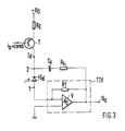
- FIG. 3 shows the circuit according to the invention, which differs from the circuit according to FIG. 1 by a schematically indicated transistor circuit instead of the resistor R V.
- This consists of a bipolar pnp transistor T, the emitter of which is connected via an emitter resistor R E to the supply voltage source U O and the collector of which is connected to terminal 2 of the photodiode.
- the transistor circuit thus limits the current I d in such a way that operating points at which I max would be exceeded do not arise. Without any control or switching processes, it is ensured that at high light levels the operating points are in the range of the steep rise in the characteristic curves (AP8, AP9). In other words: with increasing light level, the diode current I d does not increase, as would be the case with the straight line through the operating points AP1 to AP3, but the current is limited to an acceptable value, and the voltage at the photodiode becomes from the negative range inverted in the positive range.
- the operating point shift described with reference to FIG. 2 can also be effected by changing another parameter, namely by changing the bias voltage U0. Namely, this determines at which point on the abscissa a straight line defined by an ohmic resistance with regard to its slope intersects the abscissa, regardless of the slope of the straight line. This intersection is designated in Fig. 2 with U '.
- U ' With reference to FIG. 2 it is easy to see that by means of a control which, with increasing light levels, shifts the point U 'of the straight line passing through AP1 to AP3 and thus this straight line itself to the right, it can be achieved that working points such as AP3, in which I max is exceeded, avoided.
- the current-limiting element in the DC circuit of the photodiode that is to say the resistor R V or the transistor circuit, could in principle also be located on the other side of the photodiode PD in the DC circuit.
- an inductance can be connected between R V and the connection 2 of the photodiode in order to reduce the influence of stray capacitances of R V on the overall circuit.
Landscapes
- Physics & Mathematics (AREA)
- Electromagnetism (AREA)
- Engineering & Computer Science (AREA)
- Computer Networks & Wireless Communication (AREA)
- Signal Processing (AREA)
- Amplifiers (AREA)
- Optical Communication System (AREA)
Applications Claiming Priority (2)
| Application Number | Priority Date | Filing Date | Title |
|---|---|---|---|
| DE3832857 | 1988-09-28 | ||
| DE3832857A DE3832857A1 (de) | 1988-09-28 | 1988-09-28 | Optischer empfaenger mit erweitertem dynamikbereich |
Publications (3)
| Publication Number | Publication Date |
|---|---|
| EP0361342A2 true EP0361342A2 (fr) | 1990-04-04 |
| EP0361342A3 EP0361342A3 (fr) | 1991-08-21 |
| EP0361342B1 EP0361342B1 (fr) | 1994-12-21 |
Family
ID=6363859
Family Applications (1)
| Application Number | Title | Priority Date | Filing Date |
|---|---|---|---|
| EP89117625A Expired - Lifetime EP0361342B1 (fr) | 1988-09-28 | 1989-09-23 | Récepteur optique à dynamique élargie |
Country Status (5)
| Country | Link |
|---|---|
| US (1) | US5008524A (fr) |
| EP (1) | EP0361342B1 (fr) |
| JP (1) | JPH0736538B2 (fr) |
| DE (2) | DE3832857A1 (fr) |
| ES (1) | ES2068866T3 (fr) |
Families Citing this family (21)
| Publication number | Priority date | Publication date | Assignee | Title |
|---|---|---|---|---|
| SE467131B (sv) * | 1990-07-19 | 1992-05-25 | Ericsson Telefon Ab L M | Ingaangssteg foer optomottagare |
| US5091640A (en) * | 1991-06-24 | 1992-02-25 | Square D Company | Phase advance for ambient light suppression in phototransistors |
| DE4235321A1 (de) * | 1992-10-20 | 1994-04-21 | Sel Alcatel Ag | Optischer Empfänger mit Frequenzweiche |
| US5442321A (en) * | 1993-07-08 | 1995-08-15 | Anadigics, Inc. | Automatic transimpedance control amplifier |
| US5455705A (en) * | 1994-03-14 | 1995-10-03 | Analog Devices, Inc. | Transimpedance amplifier for optical receiver |
| US5790295A (en) * | 1995-08-28 | 1998-08-04 | Apple Computer, Inc. | Gated integrator preamplifier for infrared data networks |
| US5734300A (en) * | 1996-05-17 | 1998-03-31 | Lucent Technologies, Inc. | Optical receiver preamplifier dynamic range enhancing circuit and method |
| JP3437917B2 (ja) * | 1997-09-26 | 2003-08-18 | シャープ株式会社 | 受光増幅装置 |
| US6340916B1 (en) * | 2000-09-21 | 2002-01-22 | Telecommunications Laboratories, Chunghwa Telecom Co., Ltd. | Ransimpedance amplifier circuit |
| US6756578B1 (en) | 2002-01-17 | 2004-06-29 | Trimble Navigation Limited | Photocell bias circuit |
| US7068951B2 (en) * | 2002-04-11 | 2006-06-27 | Optical Communication Products, Inc. | Optical signal receiver with RPM, data and data bar output |
| US7146231B2 (en) | 2002-10-22 | 2006-12-05 | Fisher-Rosemount Systems, Inc.. | Smart process modules and objects in process plants |
| US9983559B2 (en) | 2002-10-22 | 2018-05-29 | Fisher-Rosemount Systems, Inc. | Updating and utilizing dynamic process simulation in an operating process environment |
| US7002131B1 (en) | 2003-01-24 | 2006-02-21 | Jds Uniphase Corporation | Methods, systems and apparatus for measuring average received optical power |
| US7215883B1 (en) | 2003-01-24 | 2007-05-08 | Jds Uniphase Corporation | Methods for determining the performance, status, and advanced failure of optical communication channels |
| US7305190B2 (en) * | 2003-05-06 | 2007-12-04 | Vitesse Semiconductor Corporation | Optical dispersion correction in transimpedance amplifiers |
| US7242871B2 (en) * | 2003-07-29 | 2007-07-10 | Harmonic Inc. | High dynamic range optical receiver |
| TWI225734B (en) * | 2003-11-04 | 2004-12-21 | Ind Tech Res Inst | Optical receiving device |
| CN102299744B (zh) * | 2011-08-23 | 2013-11-27 | 青岛海信宽带多媒体技术有限公司 | 具有强光保护功能的光模块 |
| US9106191B2 (en) * | 2012-05-02 | 2015-08-11 | Adaptive I/O Technologies, Inc. | Diode enhanced amplifier circuits and methods thereof |
| US12250502B2 (en) * | 2022-04-05 | 2025-03-11 | University Of Southern California | Remotely biasing, controlling, and monitoring a network routing node based on remotely provided optical signals |
Family Cites Families (4)
| Publication number | Priority date | Publication date | Assignee | Title |
|---|---|---|---|---|
| US4498001A (en) * | 1982-07-26 | 1985-02-05 | At&T Bell Laboratories | Transimpedance amplifier for optical receivers |
| US4759081A (en) * | 1984-04-26 | 1988-07-19 | Alcatel N.V. | Optical receiver |
| DE3633984A1 (de) * | 1986-10-06 | 1988-04-07 | Standard Elektrik Lorenz Ag | Optischer empfaenger mit erweitertem dynamikbereich |
| DE3806283A1 (de) * | 1988-02-27 | 1989-09-07 | Telefunken Electronic Gmbh | Optoelektronischer transimpedanz-verstaerker |
-
1988
- 1988-09-28 DE DE3832857A patent/DE3832857A1/de not_active Withdrawn
-
1989
- 1989-09-18 US US07/408,626 patent/US5008524A/en not_active Expired - Lifetime
- 1989-09-23 DE DE58908797T patent/DE58908797D1/de not_active Expired - Fee Related
- 1989-09-23 EP EP89117625A patent/EP0361342B1/fr not_active Expired - Lifetime
- 1989-09-23 ES ES89117625T patent/ES2068866T3/es not_active Expired - Lifetime
- 1989-09-28 JP JP1250812A patent/JPH0736538B2/ja not_active Expired - Fee Related
Also Published As
| Publication number | Publication date |
|---|---|
| EP0361342B1 (fr) | 1994-12-21 |
| US5008524A (en) | 1991-04-16 |
| JPH02121536A (ja) | 1990-05-09 |
| ES2068866T3 (es) | 1995-05-01 |
| JPH0736538B2 (ja) | 1995-04-19 |
| EP0361342A3 (fr) | 1991-08-21 |
| DE3832857A1 (de) | 1990-03-29 |
| DE58908797D1 (de) | 1995-02-02 |
Similar Documents
| Publication | Publication Date | Title |
|---|---|---|
| EP0361342B1 (fr) | Récepteur optique à dynamique élargie | |
| DE3233146C2 (fr) | ||
| DE3101296C2 (fr) | ||
| EP1622257B1 (fr) | Amplificateur pour convertir un signal de courant d'un récepteur optique en un signal de tension | |
| DE69219359T2 (de) | Transimpedanzverstärker | |
| DE3325420C2 (fr) | ||
| EP0313914B1 (fr) | Circuit comportant un préamplificateur connecté à un transducteur opto-électrique | |
| DE68919704T2 (de) | Strom-Spannungswandler. | |
| DE2240971C3 (de) | Torschaltung | |
| DE2542403A1 (de) | Komparatorschaltung | |
| DE602004009919T2 (de) | Schaltung für einen verbesserten differenzialverstärker und andere anwendungen | |
| DE1905993A1 (de) | Regeleinrichtung | |
| DE69729914T2 (de) | Verstärker mit negativer Rückkopplung | |
| DE3231829C2 (fr) | ||
| DE1034699B (de) | Schaltung zur selbsttaetigen Pegelregelung in Traegerfrequenz-Telefoniesystemen | |
| EP0359836B1 (fr) | Circuit comportant un amplificateur connecté à un transducteur opto-électrique | |
| DE2308835C3 (de) | Regelbarer Verstärker für elektrische Signale | |
| DE1085914B (de) | Transistorschaltung zum Zufuehren von Saegezahnstroemen an einen Belastungswiderstand | |
| DE2456375C2 (fr) | ||
| DE1909721B2 (de) | Schaltungsanordnung zur gleichspannungsteilung | |
| DE69117032T2 (de) | Endstufe mit dem Verstärkungsfaktor Eins insbesondere für monolithisch integrierbare Leistungsverstärker | |
| DE3009299A1 (de) | Hochfrequenzverstaerker mit verstaerkungsregelung | |
| DE3223218C2 (de) | Transimpedanz-Verstärker | |
| DE1951295B2 (de) | Regelbarer transistorverstaerker | |
| DE2810167A1 (de) | Transistorverstaerker |
Legal Events
| Date | Code | Title | Description |
|---|---|---|---|
| PUAI | Public reference made under article 153(3) epc to a published international application that has entered the european phase |
Free format text: ORIGINAL CODE: 0009012 |
|
| AK | Designated contracting states |
Kind code of ref document: A2 Designated state(s): AT BE CH DE ES FR GB IT LI NL SE |
|
| PUAL | Search report despatched |
Free format text: ORIGINAL CODE: 0009013 |
|
| AK | Designated contracting states |
Kind code of ref document: A3 Designated state(s): AT BE CH DE ES FR GB IT LI NL SE |
|
| 17P | Request for examination filed |
Effective date: 19911004 |
|
| RAP3 | Party data changed (applicant data changed or rights of an application transferred) |
Owner name: ALCATEL SEL AKTIENGESELLSCHAFT |
|
| 17Q | First examination report despatched |
Effective date: 19931126 |
|
| GRAA | (expected) grant |
Free format text: ORIGINAL CODE: 0009210 |
|
| AK | Designated contracting states |
Kind code of ref document: B1 Designated state(s): CH DE ES FR GB IT LI NL SE |
|
| EAL | Se: european patent in force in sweden |
Ref document number: 89117625.7 |
|
| REF | Corresponds to: |
Ref document number: 58908797 Country of ref document: DE Date of ref document: 19950202 |
|
| ITF | It: translation for a ep patent filed | ||
| GBT | Gb: translation of ep patent filed (gb section 77(6)(a)/1977) |
Effective date: 19950126 |
|
| ET | Fr: translation filed | ||
| REG | Reference to a national code |
Ref country code: ES Ref legal event code: FG2A Ref document number: 2068866 Country of ref document: ES Kind code of ref document: T3 |
|
| PLBE | No opposition filed within time limit |
Free format text: ORIGINAL CODE: 0009261 |
|
| STAA | Information on the status of an ep patent application or granted ep patent |
Free format text: STATUS: NO OPPOSITION FILED WITHIN TIME LIMIT |
|
| 26N | No opposition filed | ||
| PGFP | Annual fee paid to national office [announced via postgrant information from national office to epo] |
Ref country code: CH Payment date: 19990816 Year of fee payment: 11 |
|
| PGFP | Annual fee paid to national office [announced via postgrant information from national office to epo] |
Ref country code: NL Payment date: 19990819 Year of fee payment: 11 |
|
| PG25 | Lapsed in a contracting state [announced via postgrant information from national office to epo] |
Ref country code: LI Free format text: LAPSE BECAUSE OF NON-PAYMENT OF DUE FEES Effective date: 20000930 Ref country code: CH Free format text: LAPSE BECAUSE OF NON-PAYMENT OF DUE FEES Effective date: 20000930 |
|
| PG25 | Lapsed in a contracting state [announced via postgrant information from national office to epo] |
Ref country code: NL Free format text: LAPSE BECAUSE OF NON-PAYMENT OF DUE FEES Effective date: 20010401 |
|
| REG | Reference to a national code |
Ref country code: CH Ref legal event code: PL |
|
| NLV4 | Nl: lapsed or anulled due to non-payment of the annual fee |
Effective date: 20010401 |
|
| REG | Reference to a national code |
Ref country code: GB Ref legal event code: IF02 |
|
| PGFP | Annual fee paid to national office [announced via postgrant information from national office to epo] |
Ref country code: SE Payment date: 20020829 Year of fee payment: 14 |
|
| PGFP | Annual fee paid to national office [announced via postgrant information from national office to epo] |
Ref country code: ES Payment date: 20020923 Year of fee payment: 14 |
|
| PGFP | Annual fee paid to national office [announced via postgrant information from national office to epo] |
Ref country code: GB Payment date: 20030822 Year of fee payment: 15 |
|
| PGFP | Annual fee paid to national office [announced via postgrant information from national office to epo] |
Ref country code: DE Payment date: 20030825 Year of fee payment: 15 |
|
| PGFP | Annual fee paid to national office [announced via postgrant information from national office to epo] |
Ref country code: FR Payment date: 20030827 Year of fee payment: 15 |
|
| PG25 | Lapsed in a contracting state [announced via postgrant information from national office to epo] |
Ref country code: SE Free format text: LAPSE BECAUSE OF NON-PAYMENT OF DUE FEES Effective date: 20030924 Ref country code: ES Free format text: LAPSE BECAUSE OF NON-PAYMENT OF DUE FEES Effective date: 20030924 |
|
| EUG | Se: european patent has lapsed | ||
| PG25 | Lapsed in a contracting state [announced via postgrant information from national office to epo] |
Ref country code: GB Free format text: LAPSE BECAUSE OF NON-PAYMENT OF DUE FEES Effective date: 20040923 |
|
| REG | Reference to a national code |
Ref country code: ES Ref legal event code: FD2A Effective date: 20030924 |
|
| PG25 | Lapsed in a contracting state [announced via postgrant information from national office to epo] |
Ref country code: DE Free format text: LAPSE BECAUSE OF NON-PAYMENT OF DUE FEES Effective date: 20050401 |
|
| GBPC | Gb: european patent ceased through non-payment of renewal fee |
Effective date: 20040923 |
|
| PG25 | Lapsed in a contracting state [announced via postgrant information from national office to epo] |
Ref country code: FR Free format text: LAPSE BECAUSE OF NON-PAYMENT OF DUE FEES Effective date: 20050531 |
|
| REG | Reference to a national code |
Ref country code: FR Ref legal event code: ST |
|
| PG25 | Lapsed in a contracting state [announced via postgrant information from national office to epo] |
Ref country code: IT Free format text: LAPSE BECAUSE OF NON-PAYMENT OF DUE FEES;WARNING: LAPSES OF ITALIAN PATENTS WITH EFFECTIVE DATE BEFORE 2007 MAY HAVE OCCURRED AT ANY TIME BEFORE 2007. THE CORRECT EFFECTIVE DATE MAY BE DIFFERENT FROM THE ONE RECORDED. Effective date: 20050923 |