EP0361399A2 - Halbleiterlaser-Vielfachanordnung, die Laser mit Reflexionsmitteln enthält, die verschiedene Wellenlängen-Selektionseigenschaften haben - Google Patents
Halbleiterlaser-Vielfachanordnung, die Laser mit Reflexionsmitteln enthält, die verschiedene Wellenlängen-Selektionseigenschaften haben Download PDFInfo
- Publication number
- EP0361399A2 EP0361399A2 EP89117766A EP89117766A EP0361399A2 EP 0361399 A2 EP0361399 A2 EP 0361399A2 EP 89117766 A EP89117766 A EP 89117766A EP 89117766 A EP89117766 A EP 89117766A EP 0361399 A2 EP0361399 A2 EP 0361399A2
- Authority
- EP
- European Patent Office
- Prior art keywords
- semiconductor laser
- laser array
- array according
- quantum
- lasers
- Prior art date
- Legal status (The legal status is an assumption and is not a legal conclusion. Google has not performed a legal analysis and makes no representation as to the accuracy of the status listed.)
- Ceased
Links
Images


Classifications
-
- H—ELECTRICITY
- H01—ELECTRIC ELEMENTS
- H01S—DEVICES USING THE PROCESS OF LIGHT AMPLIFICATION BY STIMULATED EMISSION OF RADIATION [LASER] TO AMPLIFY OR GENERATE LIGHT; DEVICES USING STIMULATED EMISSION OF ELECTROMAGNETIC RADIATION IN WAVE RANGES OTHER THAN OPTICAL
- H01S5/00—Semiconductor lasers
- H01S5/10—Construction or shape of the optical resonator, e.g. extended or external cavity, coupled cavities, bent-guide, varying width, thickness or composition of the active region
- H01S5/12—Construction or shape of the optical resonator, e.g. extended or external cavity, coupled cavities, bent-guide, varying width, thickness or composition of the active region the resonator having a periodic structure, e.g. in distributed feedback [DFB] lasers
- H01S5/125—Distributed Bragg reflector [DBR] lasers
-
- B—PERFORMING OPERATIONS; TRANSPORTING
- B82—NANOTECHNOLOGY
- B82Y—SPECIFIC USES OR APPLICATIONS OF NANOSTRUCTURES; MEASUREMENT OR ANALYSIS OF NANOSTRUCTURES; MANUFACTURE OR TREATMENT OF NANOSTRUCTURES
- B82Y20/00—Nanooptics, e.g. quantum optics or photonic crystals
-
- H—ELECTRICITY
- H01—ELECTRIC ELEMENTS
- H01S—DEVICES USING THE PROCESS OF LIGHT AMPLIFICATION BY STIMULATED EMISSION OF RADIATION [LASER] TO AMPLIFY OR GENERATE LIGHT; DEVICES USING STIMULATED EMISSION OF ELECTROMAGNETIC RADIATION IN WAVE RANGES OTHER THAN OPTICAL
- H01S5/00—Semiconductor lasers
- H01S5/10—Construction or shape of the optical resonator, e.g. extended or external cavity, coupled cavities, bent-guide, varying width, thickness or composition of the active region
- H01S5/12—Construction or shape of the optical resonator, e.g. extended or external cavity, coupled cavities, bent-guide, varying width, thickness or composition of the active region the resonator having a periodic structure, e.g. in distributed feedback [DFB] lasers
-
- H—ELECTRICITY
- H01—ELECTRIC ELEMENTS
- H01S—DEVICES USING THE PROCESS OF LIGHT AMPLIFICATION BY STIMULATED EMISSION OF RADIATION [LASER] TO AMPLIFY OR GENERATE LIGHT; DEVICES USING STIMULATED EMISSION OF ELECTROMAGNETIC RADIATION IN WAVE RANGES OTHER THAN OPTICAL
- H01S5/00—Semiconductor lasers
- H01S5/10—Construction or shape of the optical resonator, e.g. extended or external cavity, coupled cavities, bent-guide, varying width, thickness or composition of the active region
- H01S5/18—Surface-emitting [SE] lasers, e.g. having both horizontal and vertical cavities
- H01S5/185—Surface-emitting [SE] lasers, e.g. having both horizontal and vertical cavities having only horizontal cavities, e.g. horizontal cavity surface-emitting lasers [HCSEL]
- H01S5/187—Surface-emitting [SE] lasers, e.g. having both horizontal and vertical cavities having only horizontal cavities, e.g. horizontal cavity surface-emitting lasers [HCSEL] using Bragg reflection
-
- H—ELECTRICITY
- H01—ELECTRIC ELEMENTS
- H01S—DEVICES USING THE PROCESS OF LIGHT AMPLIFICATION BY STIMULATED EMISSION OF RADIATION [LASER] TO AMPLIFY OR GENERATE LIGHT; DEVICES USING STIMULATED EMISSION OF ELECTROMAGNETIC RADIATION IN WAVE RANGES OTHER THAN OPTICAL
- H01S5/00—Semiconductor lasers
- H01S5/30—Structure or shape of the active region; Materials used for the active region
- H01S5/34—Structure or shape of the active region; Materials used for the active region comprising quantum well or superlattice structures, e.g. single quantum well [SQW] lasers, multiple quantum well [MQW] lasers or graded index separate confinement heterostructure [GRINSCH] lasers
-
- H—ELECTRICITY
- H01—ELECTRIC ELEMENTS
- H01S—DEVICES USING THE PROCESS OF LIGHT AMPLIFICATION BY STIMULATED EMISSION OF RADIATION [LASER] TO AMPLIFY OR GENERATE LIGHT; DEVICES USING STIMULATED EMISSION OF ELECTROMAGNETIC RADIATION IN WAVE RANGES OTHER THAN OPTICAL
- H01S5/00—Semiconductor lasers
- H01S5/40—Arrangement of two or more semiconductor lasers, not provided for in groups H01S5/02 - H01S5/30
- H01S5/4025—Array arrangements, e.g. constituted by discrete laser diodes or laser bar
- H01S5/4031—Edge-emitting structures
- H01S5/4043—Edge-emitting structures with vertically stacked active layers
-
- H—ELECTRICITY
- H01—ELECTRIC ELEMENTS
- H01S—DEVICES USING THE PROCESS OF LIGHT AMPLIFICATION BY STIMULATED EMISSION OF RADIATION [LASER] TO AMPLIFY OR GENERATE LIGHT; DEVICES USING STIMULATED EMISSION OF ELECTROMAGNETIC RADIATION IN WAVE RANGES OTHER THAN OPTICAL
- H01S5/00—Semiconductor lasers
- H01S5/02—Structural details or components not essential to laser action
- H01S5/028—Coatings ; Treatment of the laser facets, e.g. etching, passivation layers or reflecting layers
-
- H—ELECTRICITY
- H01—ELECTRIC ELEMENTS
- H01S—DEVICES USING THE PROCESS OF LIGHT AMPLIFICATION BY STIMULATED EMISSION OF RADIATION [LASER] TO AMPLIFY OR GENERATE LIGHT; DEVICES USING STIMULATED EMISSION OF ELECTROMAGNETIC RADIATION IN WAVE RANGES OTHER THAN OPTICAL
- H01S5/00—Semiconductor lasers
- H01S5/30—Structure or shape of the active region; Materials used for the active region
- H01S5/34—Structure or shape of the active region; Materials used for the active region comprising quantum well or superlattice structures, e.g. single quantum well [SQW] lasers, multiple quantum well [MQW] lasers or graded index separate confinement heterostructure [GRINSCH] lasers
- H01S5/3428—Structure or shape of the active region; Materials used for the active region comprising quantum well or superlattice structures, e.g. single quantum well [SQW] lasers, multiple quantum well [MQW] lasers or graded index separate confinement heterostructure [GRINSCH] lasers layer orientation perpendicular to the substrate
-
- H—ELECTRICITY
- H01—ELECTRIC ELEMENTS
- H01S—DEVICES USING THE PROCESS OF LIGHT AMPLIFICATION BY STIMULATED EMISSION OF RADIATION [LASER] TO AMPLIFY OR GENERATE LIGHT; DEVICES USING STIMULATED EMISSION OF ELECTROMAGNETIC RADIATION IN WAVE RANGES OTHER THAN OPTICAL
- H01S5/00—Semiconductor lasers
- H01S5/40—Arrangement of two or more semiconductor lasers, not provided for in groups H01S5/02 - H01S5/30
- H01S5/4025—Array arrangements, e.g. constituted by discrete laser diodes or laser bar
- H01S5/4087—Array arrangements, e.g. constituted by discrete laser diodes or laser bar emitting more than one wavelength
Definitions
- This invention relates to a semiconductor laser array which emits a plurality of laser lights having different wavelengths and which is suitable for use in transmission or processing of multi-wavelength-light information.
- Conventional semiconductor laser arrays of this kind are known in which a plurality of semiconductor lasers having a distributed feed back (DFB) structure of distributed Bragg reflector (DBR) are formed on a substrate in a monolithic construction manner and the diffraction gratings for the respective lasers are formed with different pitches, and which thereby emits a plurality of laser light beams having different wavelengths.
- DBR distributed feed back
- the difference between the wavelengths of the lights emitted from the lasers is small and is at most several nanometers if the laser array is designed to make the characteristics of the lasers uniform.
- a known type of laser array designed to emit a plurality of laser lights having wavelengths greatly different from each other based on forming an active layer of each laser in a quantum well structure is proposed in USP No.4,817,110, particularly in the statement between line 16 in col. 21 and line 6 in col. 24 of the specification thereof.
- This laser array is constructed in such a manner that a plurality of semiconductor lasers having active layers having a quantum well structure are arranged on a substrate so that internal losses or reflection losses of the respective layers are different from each other.
- the mirror loss of the respective laser may be varied by varying the reflectivity of the mirror of the respective laser by such as a method of end facet coating.
- the mirror loss of this laser array is not determined with respect to the oscillation wavelength of each laser light, and it is not assured that all the lasers can effect oscillation under suitable conditions. For this reason, there is a risk of a reduction in the emission efficiency or dispersion of the characteristics of the lasers.
- a semiconductor laser array comprising a plurality of lasers having, within an active layer, quantum well structure with at least two quantum well levels for generating, respectively and independently of each other, laser light beams of mutually different oscillation wavelengths.
- the reflecting means have wavelength selection properties corresponding to each of the mutually different oscillation wavelengths.
- a semiconductor laser array which comprises first and second semiconductor lasers and first and second reflecting means provided, respectively, for the first and second semiconductor lasers.
- Each of the semiconductor lasers has, within an active layer, a quantum well structure with at least two quantum levels,
- the first and second semiconductor lasers are constructed to emit light having first and second wavelengths, respectively.
- the active layers of the two semiconductor lasers are formed together in a substrate in a monolithic construction.
- the first reflecting means are constructed to reflect light of the first wavelength with a reflectance which is higher than that with which the first reflecting means reflects light having the second wavelength.
- the second reflecting means are constructed to reflect light of the second wavelength with a reflectance with is higher than that with which the second reflecting means reflects light having the first wavelength.
- Fig. 1 schematically shows in perspective essential portions of a semiconductor laser array to which a distributed reflection type of laser structure is applied and which represents a first embodiment of the present invention.
- This semiconductor laser array is constructed by successively forming by epitaxial growth on an n+-GaAs substrate 1 (thickness: about 100 ⁇ m) an n-Al 0.5 Ga 0.5 As clad layer 2 (thickness: 1.5 ⁇ m), an active layer 3 (thickness: 0.1 ⁇ m), a p-Al 0.2 Ga 0.8 As optical waveguide layer 4 (thickness: 0.1 ⁇ m) on which diffraction gratings 4i and 4ii, corresponding to lasers (i) and (ii) are formed, a p-Al 0.5 Ga 0.5 As clad layer 5 formed as ridge structures (thickness: 1.5 ⁇ m) and a p+-GaAs cap layer 6 also formed as ridge structures on the laser 5 (thickness: 0.5 ⁇ m).
- a common electrode 9 is formed on the bottom surface of the substrate 1 and is connected to ground.
- electrodes 81 and 82 are formed over the cap layer 6 independently of each other; and these electrodes are connected to associated current sources R1, V1, and R2, V2, respectively.
- a reference character 7 denotes an insulating layer between the electrodes 81 and 82 on the one side and the waveguide layer 4, the clad layer 5, and the cap layer 6 on the other side.
- the active layer 3 is formed of an Al 0.3 Ga 0.7 As light confinement layer 11 (thickness: 300 ⁇ ), a GaAs quantum well (I) layer 12 (150 ⁇ ), an AlGaAs barrier layer 13 (thickness: 100 ⁇ ), an Al 0.09 Ga 0.91 As quantum well (II) layer 14 and an Al 0.3 Ga 0.7 As light confinement layer 15 (thickness: 300 ⁇ ).
- the energy gaps of the quantum wells I and II are 1.444 eV and 1.554 eV, respectively, and the oscillation wavelengths thereat are 869 nm and 808 nm.
- Lights beams can be generated in the layers 12 and 14 independently of each other because, ordinarily, there is substantially no interference between the quantum levels of the wells separated by the barrier layer 13 provided that the thickness of the barrier layer is not smaller than 100 ⁇ .
- the pitch of the diffraction grating 4i or 4ii or the equivalent refractive index of the optical waveguide 4 may be controlled.
- the pitch ⁇ i of the diffraction grating 4 formed for the laser (i) is obtained from a wavelength ⁇ i selected as desired and on the basis of an equation.. (where l is an integer which represents the diffraction order, 2n eff(i) represents the equivalent diffraction factor, and i is a symbol designating each unit semiconductor laser). Oscillation can be thereby effected stably with different values of the wavelength ⁇ i .
- each of the subscripts i in equation (1) is replaced by ii.
- the front section in which the electrodes 81 and 82 are provided is formed with a dual ridge structure (each ridge bottom width: about 2 to 5 ⁇ m) which defines an active region.
- This ridge structure is made by partially cutting the lamination to the upper surface of the optical waveguide layer 4 in a selective etching manner after all the layers have been formed.
- This partial and selective etching may be performed by a method based on a process in which a composition having a larger value of x of Al x Ga 1-x As is etched faster by NaOH and H2O2. Flat surfaces are thereby formed with ridge portions left therebetween. Additional ridge structures may be formed in the same manner.
- the diffraction gratings 4i and 4ii are formed over the optical waveguide layer 4 at the rear of the active region.
- Each diffraction grating is formed with a pitch corresponding to the desired oscillation frequency obtained from the equation (1).
- the conditions of the two beam interference exposure method for forming the resist are changed as desired.
- an SiO2 dielectric element 10 is provided lengthwise in alignment with each ridge structure.
- the active layer 3 has a type of structure including two independent quantum wells I and II equal to each other in width but different in composition.
- a plurality of quantum wells having levels with different energy gaps may be provided in the active layer 3.
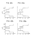
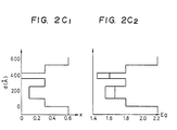
- quantum well structures having changes in composition such as those shown in Figs. 2A to 2C can be applied.
- Each of the graphs in Figs, 2A1, 2B1 and 2C1 shows changes in x of Al x Ga 1-x As (abscissa) in the direction of the thickness of the layer (ordinate) while each of the graphs in Figs. 2A2, 2B2 and 2C2 shows changes in the energy gap (abscissa) in the direction of the thickness of the layer (ordinate). That is, these Figs. show changes in the compositions and energy gaps of different types of quantum well structures.
- the quantum wells in the structure shown in Figs. 2A1 and 2A2 are equal in width but different in composition
- the quantum wells in the structure shown in Figs. 2B1 and 2B2 are different in width but equal in composition
- the quantum wells in the structure shown in Figs. 2C1 and 2C2 differ from each other in both width and composition. In either case, the energy gaps are made different from each other, as can be understood from the graph on the right-hand side.
- Each illustrated type of quantum well structure can be provided with a plurality of energy gaps and can be applied to effect oscillation with the desired wavelength by selecting the structure of the DBR region for each unit semiconductor laser or, more specifically, the pitch of the mated diffraction grating. That is, it is possible to select and utilize the desired one of a plurality of energy gaps by providing the diffraction grating pitch necessary for bragg reflection of light emitted by the energy gap necessary for oscillation with the desired wavelength.
- the number of quantum wells, the well width, the composition and so on may be selected as desired so as to maximize the gain of oscillation of light having the desired wavelength.
- the two-wavelength semiconductor laser array in accordance with this embodiment enables oscillation with a wavelength stably maintained and is therefore suitable for application to light sources for multi-wavelength-light communication.
- Figs. 3 and 4 show in perspective a second embodiment of the present invention having a DFB structure.
- Fig. 3 is a perspective view of a stage of formation of a laser array at which an optical waveguide layer 4 having two different diffraction grating sections (iii) and (iv) is formed over an active layer 3.
- the grating pitches in the sections (iii) and (iv) are selected to obtain the desired oscillation wavelengths ⁇ 3 and ⁇ 4.
- the diffraction grating pitch is set so as to satisfy the relationship defined by the equation 1.
- a clad layer and a cap layer are formed over the gratings, and a working and/or regrowth process is thereafter conducted if necessary, thereby forming a refractive index waveguide type structure.
- Independent electrodes 81 and 82 for independently driving the sections (iii) and (iv) are finally formed by deposition, thereby obtaining a semiconductor laser array such as that shown in Fig. 4. These electrodes are connected to current sources V1, R1 and V2, R2, respectively.
- the active layer 3 common to the unit semiconductor lasers of this laser array is formed to have a quantum well structure similar to that of the first embodiment and which is optimized to select the desired oscillation wavelengths ⁇ 3 and ⁇ 4.
- the above-described laser arrays are examples of monolithic semiconductor laser arrays for effecting oscillation of two laser light beams having different wavelengths.
- the number of unit semiconductor lasers integrated can be increased as desired.
- a semiconductor laser array capable of oscillating two or more laser lights having different wavelengths in accordance with the present invention is suitable for multi-wavelength-light communication requiring two or more wavelengths.
- the DBR region having the diffraction gratings is formed in the rear section alone.
- another DBR region may be formed in front of the waveguide to control the bragg reflectance by changing the length thereof. It is thereby also possible to change the threshold current or efficiency or to reduce the longitudinal mode spectrum line width.
- Each DBR region may be embedded by a regrowth process.
- Fig. 5 is a schematic plan view of a semiconductor laser array which represents a third embodiment of the present invention
- Fig. 6 is a cross-sectional view of part of the laser array shown in Fig. 5 taken along the line A-B thereof.
- the semiconductor laser array in accordance with this embodiment is constructed by successively laminating, on an n-GaAs substrate 28 (thickness: 100 ⁇ m), an n-GaAs buffer layer 29 (thickness: 0.5 ⁇ m), an n-AlGaAs clad layer 30 (thickness: 0.5 ⁇ m), an n-AlGaAs separate confinement (SC) layer 31 (thickness: 150 ⁇ ) in which the compositions is gradually changed in the direction of the thickness, an active layer 32 (thickness: 100 ⁇ ) having a GaAs single Quantum well (SQW) structure, a p-AlGaAs SC layer 33 (thickness: 150 ⁇ ) in which the compositions is gradually changed in the direction of the thickness, a p-AlGaAs clad layer 34 (thickness in a ridge structure: 1.5 ⁇ m), and a p-GaAs cap layer 37 (thickness: 0.5 ⁇ m
- current restriction and light confinement are effected by ridge structures (width of each ridge: 2.5 ⁇ m, distance between the upper end of SC layer 33 and the lower ends of ridge sides: 0.3 ⁇ m). These ridge structures define an active stripe regions 18 and 19.
- the ridge structure may be formed a process of forming the above lamination structure, etching the same so as to leave the necessary portion in the form of stripes and forming an SiN insulating layer 35, and an Au electrode 36 on each stripe.
- Au electrodes common electrode 27 and independent electrodes 36
- the composition of wells comprises GaAs
- the well width is 100 ⁇
- the composition of a barrier comprises Ga 0.7 Al 0.3 As.
- Active stripe regions 18 and 19 formed on the same substrate are provided with independent electrodes, thereby being driven independently.
- Reflecting films having spectral reflectance characteristics as shown in Figs. 7 and 8 are provided in combination with end surfaces of the active stripe regions 18 and 19. That is, reflecting film coatings 21 and 23 are respectively formed on the front and rear end surfaces of the active stripe region 18, while reflecting film coatings 22 and 24 are respectively formed on the front and rear end surfaces of the active stripe region 19.
- the reflecting films may be formed by depositing an insulating material such as Al2O3, ZrO2, Si or the like on the end surface on the basis of an electron beam deposition method.
- I-L (current-light) output characteristics of the active stripe regions 18 and 19 are exhibited as shown in Fig. 10, and substantially equal light outputs P can be obtained by equal drive currents.
- the stripes 18 and 19 enable oscillation of laser lights having wavelength of 810 nm and 870 nm by equal drive currents of 60 mA.
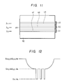
- Fig. 11 shows schematically in plan portions of a semiconductor laser array which represents a fourth embodiment of the present invention.
- the structure of the semiconductor laser array of this embodiment is substantially the same as the structure shown in Fig. 5, but differs from the same in that the active layer has a multiple quantum well structure in which GaAs wells having widths of 80 ⁇ , 55 ⁇ and 40 ⁇ , respectively, as shown in Fig. 12, are successively laminated within the SC layer.
- Reflecting film coatings 49, 50, and 51 having different reflectances as shown in Fig. 13 are formed on end surfaces opposite to light emission end surfaces.
- a reflecting film coating 48 having a low reflectance with respect to a range of wavelengths from 820 to 860 nm is formed over the light emission end surfaces.
- These reflecting films may be formed by depositing an insulating material such as Al2O3, ZrO2, Si or the like on the end surface on the basis of an electron beam deposition method.
- each laser is not limited to the ridge structure of the embodiment and may be of any type including a buried hetero- (BH) type so long as it ensures suitable effects of current restriction and light confinement.
- the crystalline material may be selected from various materials other than AlGaAs, including ordinary compound semiconductors such as InGaAsP- and AlGaInP-compounds.
- a semiconductor laser array including a plurality of semiconductor lasers each having an active layer having a quantum well structure with at least two quantum levels.
- the semiconductor lasers have reflecting means having different wavelength selection properties.
Landscapes
- Physics & Mathematics (AREA)
- Optics & Photonics (AREA)
- Condensed Matter Physics & Semiconductors (AREA)
- General Physics & Mathematics (AREA)
- Electromagnetism (AREA)
- Chemical & Material Sciences (AREA)
- Engineering & Computer Science (AREA)
- Nanotechnology (AREA)
- Life Sciences & Earth Sciences (AREA)
- Biophysics (AREA)
- Crystallography & Structural Chemistry (AREA)
- Semiconductor Lasers (AREA)
Applications Claiming Priority (4)
| Application Number | Priority Date | Filing Date | Title |
|---|---|---|---|
| JP240965/88 | 1988-09-28 | ||
| JP63240965A JP2624310B2 (ja) | 1988-09-28 | 1988-09-28 | 多波長半導体レーザ装置 |
| JP262890/88 | 1988-10-20 | ||
| JP63262890A JP2645871B2 (ja) | 1988-10-20 | 1988-10-20 | 多波長半導体レーザ装置 |
Publications (2)
| Publication Number | Publication Date |
|---|---|
| EP0361399A2 true EP0361399A2 (de) | 1990-04-04 |
| EP0361399A3 EP0361399A3 (de) | 1990-07-18 |
Family
ID=26535010
Family Applications (1)
| Application Number | Title | Priority Date | Filing Date |
|---|---|---|---|
| EP89117766A Ceased EP0361399A3 (de) | 1988-09-28 | 1989-09-26 | Halbleiterlaser-Vielfachanordnung, die Laser mit Reflexionsmitteln enthält, die verschiedene Wellenlängen-Selektionseigenschaften haben |
Country Status (2)
| Country | Link |
|---|---|
| US (1) | US4993036A (de) |
| EP (1) | EP0361399A3 (de) |
Cited By (3)
| Publication number | Priority date | Publication date | Assignee | Title |
|---|---|---|---|---|
| EP0539015A1 (de) * | 1991-10-18 | 1993-04-28 | Xerox Corporation | Halbleiterlaser zur Aussendung mehrerer Wellenlängen |
| EP0786843A1 (de) * | 1996-01-29 | 1997-07-30 | France Telecom | Mehrfachwellenlängen-Laser-Emissionsbauelement |
| EP1137134A3 (de) * | 2000-03-14 | 2004-05-12 | Kabushiki Kaisha Toshiba | Halbleiterlaservorrichtung und Herstellungsverfahren |
Families Citing this family (39)
| Publication number | Priority date | Publication date | Assignee | Title |
|---|---|---|---|---|
| FR2642228A1 (fr) * | 1989-01-20 | 1990-07-27 | Menigaux Louis | Procede de fabrication d'un dispositif semi-conducteur quasi plat susceptible d'effet laser multi-longueurs d'onde et dispositif correspondant |
| US5033053A (en) * | 1989-03-30 | 1991-07-16 | Canon Kabushiki Kaisha | Semiconductor laser device having plurality of layers for emitting lights of different wavelengths and method of driving the same |
| DE69009561T2 (de) * | 1989-03-31 | 1994-10-13 | Canon Kk | Halbleiterlaser zur selektiven Ausstrahlung von Licht mit verschiedenen Wellenlängen. |
| US5132750A (en) * | 1989-11-22 | 1992-07-21 | Daido Tokushuko Kabushiki Kaisha | Light-emitting diode having light reflecting layer |
| JPH0724324B2 (ja) * | 1990-03-16 | 1995-03-15 | 株式会社東芝 | 半導体レーザ・チップおよびその製造方法 |
| US5153688A (en) * | 1990-04-21 | 1992-10-06 | Canon Kabushiki Kaisha | Method and device for controlling interference of electron waves by light in which a transverse magnetic wave is applied |
| US5289018A (en) * | 1990-08-14 | 1994-02-22 | Canon Kabushiki Kaisha | Light emitting device utilizing cavity quantum electrodynamics |
| JPH04107976A (ja) * | 1990-08-28 | 1992-04-09 | Mitsubishi Electric Corp | 半導体レーザ装置 |
| US5224114A (en) * | 1990-11-11 | 1993-06-29 | Canon Kabushiki Kaisha | Semiconductor laser devices with a plurality of light emitting layers having different bands gaps and methods for driving the same |
| GB2260872B (en) * | 1991-09-20 | 1995-10-25 | Sharp Kk | An optical transmission system |
| US5164956A (en) * | 1991-10-21 | 1992-11-17 | The United States Of America As Represented By The Administrator Of The National Aeronautics And Space Administration | Multiperiod-grating surface-emitting lasers |
| JP3014208B2 (ja) * | 1992-02-27 | 2000-02-28 | 三菱電機株式会社 | 半導体光素子 |
| US5285468A (en) * | 1992-07-17 | 1994-02-08 | At&T Bell Laboratories | Analog optical fiber communication system, and laser adapted for use in such a system |
| US5384797A (en) * | 1992-09-21 | 1995-01-24 | Sdl, Inc. | Monolithic multi-wavelength laser diode array |
| US5311539A (en) * | 1992-11-25 | 1994-05-10 | International Business Machines Corporation | Roughened sidewall ridge for high power fundamental mode semiconductor ridge waveguide laser operation |
| US5465263A (en) * | 1992-12-12 | 1995-11-07 | Xerox Corporation | Monolithic, multiple wavelength, dual polarization laser diode arrays |
| US5307359A (en) * | 1992-12-21 | 1994-04-26 | Eastman Kodak Company | Monolithic semi-conductor laser producing blue, green and red output wavelengths |
| JPH0794781A (ja) * | 1993-09-24 | 1995-04-07 | Toshiba Corp | 面発光型半導体発光ダイオード |
| JPH08107254A (ja) * | 1994-09-14 | 1996-04-23 | Xerox Corp | マルチ波長レーザダイオードアレイ |
| JPH10117040A (ja) * | 1996-10-08 | 1998-05-06 | Nec Corp | 半導体レーザ素子及びその製造方法 |
| US6327289B1 (en) | 1997-09-02 | 2001-12-04 | Matsushita Electric Industrial Co., Ltd. | Wavelength-variable semiconductor laser, optical integrated device utilizing the same, and production method thereof |
| JP3522107B2 (ja) * | 1997-12-18 | 2004-04-26 | 日本電気株式会社 | 半導体レーザ |
| US6104739A (en) * | 1997-12-24 | 2000-08-15 | Nortel Networks Corporation | Series of strongly complex coupled DFB lasers |
| JP3847038B2 (ja) * | 1999-11-26 | 2006-11-15 | Necエレクトロニクス株式会社 | 光半導体装置およびその製造方法 |
| JP2001184698A (ja) * | 1999-12-22 | 2001-07-06 | Pioneer Electronic Corp | 光ピックアップ装置 |
| JP2001320131A (ja) * | 2000-03-01 | 2001-11-16 | Sony Corp | 多波長半導体レーザ素子アレイ及びその作製方法 |
| CA2363149A1 (en) * | 2001-11-16 | 2003-05-16 | Photonami Inc. | Surface emitting dfb laser structures for broadband communication systems and array of same |
| CN1774845B (zh) * | 2004-03-23 | 2010-10-06 | 日本电信电话株式会社 | Dbr型波长可变光源 |
| JP2006013191A (ja) * | 2004-06-28 | 2006-01-12 | Fujitsu Ltd | 光半導体素子 |
| JP2006093466A (ja) * | 2004-09-24 | 2006-04-06 | Toshiba Corp | 多波長半導体レーザ素子および多波長半導体レーザ装置 |
| US7313158B2 (en) * | 2005-02-08 | 2007-12-25 | Photodigm, Inc. | Integrated high speed modulator for grating-outcoupled surface emitting lasers |
| JP4908837B2 (ja) * | 2005-12-13 | 2012-04-04 | キヤノン株式会社 | 発光素子アレイ及び画像形成装置 |
| JP2007311522A (ja) * | 2006-05-18 | 2007-11-29 | Mitsubishi Electric Corp | 半導体レーザ |
| JP5190115B2 (ja) * | 2007-09-11 | 2013-04-24 | ビノプティクス・コーポレイション | 多重キャビティエッチファセットdfbレーザ |
| WO2014164960A1 (en) * | 2013-03-12 | 2014-10-09 | Applied Physical Electronics, Lc | High average power integrated optical waveguide laser |
| KR102475891B1 (ko) * | 2015-10-08 | 2022-12-12 | 삼성전자주식회사 | 측면 발광 레이저 광원, 및 이를 포함한 3차원 영상 획득 장치 |
| JP6849371B2 (ja) * | 2015-10-08 | 2021-03-24 | 三星電子株式会社Samsung Electronics Co.,Ltd. | 側面発光レーザ光源、及びそれを含む三次元映像取得装置 |
| IT201700087052A1 (it) * | 2017-07-28 | 2019-01-28 | Prima Electro S P A | Procedimento di fabbricazione di un diodo laser a semiconduttore, e diodo laser |
| DE102020133174A1 (de) | 2020-12-11 | 2022-06-15 | OSRAM Opto Semiconductors Gesellschaft mit beschränkter Haftung | Halbleiterlaser und verfahren zur herstellung eines halbleiterlasers |
Family Cites Families (14)
| Publication number | Priority date | Publication date | Assignee | Title |
|---|---|---|---|---|
| JPS5511341A (en) * | 1978-07-07 | 1980-01-26 | Sanyo Electric Co Ltd | Manufacturing method of magnetoelectric converter element |
| US4318058A (en) * | 1979-04-24 | 1982-03-02 | Nippon Electric Co., Ltd. | Semiconductor diode laser array |
| JPS5821888A (ja) * | 1981-07-31 | 1983-02-08 | Omron Tateisi Electronics Co | 可変波長半導体レ−ザ |
| JPS58110087A (ja) * | 1981-12-24 | 1983-06-30 | Fujitsu Ltd | 半導体レ−ザ装置 |
| US4648905A (en) * | 1983-01-31 | 1987-03-10 | Union Camp Corporation | Aqueous printing ink |
| JPS60236276A (ja) * | 1984-05-09 | 1985-11-25 | Mitsubishi Electric Corp | 多波長半導体レ−ザ |
| US4740978A (en) * | 1985-03-14 | 1988-04-26 | Max-Planck-Gesellschaft Zur Foerderung Der Wissenschaften E.V. | Integrated quantum well lasers having uniform thickness lasing regions for wavelength multiplexing |
| EP0194335B1 (de) * | 1985-03-14 | 1991-01-02 | Max-Planck-Gesellschaft zur Förderung der Wissenschaften e.V. | Halbleiterlaser-Vorrichtungen |
| JPS61251183A (ja) * | 1985-04-30 | 1986-11-08 | Fujitsu Ltd | 2周波半導体レ−ザ |
| DE3751535T2 (de) * | 1986-07-25 | 1996-02-22 | Mitsubishi Electric Corp | Halbleiterlaser. |
| JPH0642291B2 (ja) * | 1986-08-25 | 1994-06-01 | キヤノン株式会社 | 集積化光ヘツド |
| GB2197531B (en) * | 1986-11-08 | 1991-02-06 | Stc Plc | Distributed feedback laser |
| JPS63148692A (ja) * | 1986-12-12 | 1988-06-21 | Nec Corp | 多波長分布ブラツグ反射型半導体レ−ザ・アレ− |
| JP2543551B2 (ja) * | 1987-12-28 | 1996-10-16 | キヤノン株式会社 | 半導体レ―ザ― |
-
1989
- 1989-09-26 EP EP89117766A patent/EP0361399A3/de not_active Ceased
- 1989-09-26 US US07/412,983 patent/US4993036A/en not_active Expired - Lifetime
Cited By (5)
| Publication number | Priority date | Publication date | Assignee | Title |
|---|---|---|---|---|
| EP0539015A1 (de) * | 1991-10-18 | 1993-04-28 | Xerox Corporation | Halbleiterlaser zur Aussendung mehrerer Wellenlängen |
| EP0786843A1 (de) * | 1996-01-29 | 1997-07-30 | France Telecom | Mehrfachwellenlängen-Laser-Emissionsbauelement |
| FR2744292A1 (fr) * | 1996-01-29 | 1997-08-01 | Menigaux Louis | Composant d'emission laser multi-longueur d'onde |
| US5930278A (en) * | 1996-01-29 | 1999-07-27 | France Telecom | Multi-wavelength laser-emitting component |
| EP1137134A3 (de) * | 2000-03-14 | 2004-05-12 | Kabushiki Kaisha Toshiba | Halbleiterlaservorrichtung und Herstellungsverfahren |
Also Published As
| Publication number | Publication date |
|---|---|
| US4993036A (en) | 1991-02-12 |
| EP0361399A3 (de) | 1990-07-18 |
Similar Documents
| Publication | Publication Date | Title |
|---|---|---|
| US4993036A (en) | Semiconductor laser array including lasers with reflecting means having different wavelength selection properties | |
| US5784399A (en) | Polarization mode selection by distributed Bragg reflector in a quantum well laser | |
| US7106772B2 (en) | Distributed feedback semiconductor laser | |
| US6775427B2 (en) | Laterally coupled wave guides | |
| US6760359B2 (en) | Grating-outcoupled surface-emitting lasers with flared gain regions | |
| JP3714430B2 (ja) | 分布帰還型半導体レーザ装置 | |
| EP0390167B1 (de) | Halbleiterlaser-Vorrichtung mit mehreren Schichten zur Ausstrahlung von Licht mit verschiedenen Wellenlängen und Verfahren zu deren Betrieb | |
| US6560262B1 (en) | Vertical cavity surface emitting laser array and a process for making same | |
| US7450624B2 (en) | Grating—outcoupled surface-emitting lasers | |
| KR100731241B1 (ko) | 반도체 레이저 디바이스 및 반도체 레이저의 제조 방법 | |
| US6888874B2 (en) | Single-wavelength, unequal-length-multi-cavity grating-outcoupled surface emitting laser with staggered tuned distributed Bragg reflectors | |
| US6810067B2 (en) | Single mode grating-outcoupled surface emitting laser with broadband and narrow-band DBR reflectors | |
| JP5143985B2 (ja) | 分布帰還型半導体レーザ素子 | |
| US20040013144A1 (en) | Complex-coupled distributed feedback semiconductor laser device | |
| US6647048B2 (en) | Grating-outcoupled surface-emitting lasers using quantum wells with thickness and composition variation | |
| US6636547B2 (en) | Multiple grating-outcoupled surface-emitting lasers | |
| JP2624310B2 (ja) | 多波長半導体レーザ装置 | |
| JP2645871B2 (ja) | 多波長半導体レーザ装置 | |
| JP2003152272A (ja) | 分散位相シフト構造分布帰還型半導体レーザ | |
| KR20060132483A (ko) | 다파장 레이저 다이오드 | |
| JPH0823137A (ja) | レーザダイオードアレイ | |
| JPH11307856A (ja) | 分布帰還型レーザ及びその製造方法 | |
| JPH11307874A (ja) | 光アイソレータ、分布帰還型レーザ及び光集積素子 | |
| EP0525971B1 (de) | Halbleitervorrichtung und Verfahren zur Herstellung derselben | |
| JP2913946B2 (ja) | 量子井戸型半導体レーザ |
Legal Events
| Date | Code | Title | Description |
|---|---|---|---|
| PUAI | Public reference made under article 153(3) epc to a published international application that has entered the european phase |
Free format text: ORIGINAL CODE: 0009012 |
|
| AK | Designated contracting states |
Kind code of ref document: A2 Designated state(s): DE FR GB |
|
| PUAL | Search report despatched |
Free format text: ORIGINAL CODE: 0009013 |
|
| AK | Designated contracting states |
Kind code of ref document: A3 Designated state(s): DE FR GB |
|
| 17P | Request for examination filed |
Effective date: 19901207 |
|
| 17Q | First examination report despatched |
Effective date: 19920901 |
|
| APAB | Appeal dossier modified |
Free format text: ORIGINAL CODE: EPIDOS NOAPE |
|
| STAA | Information on the status of an ep patent application or granted ep patent |
Free format text: STATUS: THE APPLICATION HAS BEEN REFUSED |
|
| 18R | Application refused |
Effective date: 19981216 |
|
| APAF | Appeal reference modified |
Free format text: ORIGINAL CODE: EPIDOSCREFNE |