EP0361651B1 - Optisches Element und Verfahren zum Modulieren von Licht unter Verwendung desselben - Google Patents
Optisches Element und Verfahren zum Modulieren von Licht unter Verwendung desselben Download PDFInfo
- Publication number
- EP0361651B1 EP0361651B1 EP89307331A EP89307331A EP0361651B1 EP 0361651 B1 EP0361651 B1 EP 0361651B1 EP 89307331 A EP89307331 A EP 89307331A EP 89307331 A EP89307331 A EP 89307331A EP 0361651 B1 EP0361651 B1 EP 0361651B1
- Authority
- EP
- European Patent Office
- Prior art keywords
- quantum well
- optical element
- light
- layers
- signal light
- Prior art date
- Legal status (The legal status is an assumption and is not a legal conclusion. Google has not performed a legal analysis and makes no representation as to the accuracy of the status listed.)
- Expired - Lifetime
Links
Images


Classifications
-
- B—PERFORMING OPERATIONS; TRANSPORTING
- B82—NANOTECHNOLOGY
- B82Y—SPECIFIC USES OR APPLICATIONS OF NANOSTRUCTURES; MEASUREMENT OR ANALYSIS OF NANOSTRUCTURES; MANUFACTURE OR TREATMENT OF NANOSTRUCTURES
- B82Y20/00—Nanooptics, e.g. quantum optics or photonic crystals
-
- G—PHYSICS
- G02—OPTICS
- G02F—OPTICAL DEVICES OR ARRANGEMENTS FOR THE CONTROL OF LIGHT BY MODIFICATION OF THE OPTICAL PROPERTIES OF THE MEDIA OF THE ELEMENTS INVOLVED THEREIN; NON-LINEAR OPTICS; FREQUENCY-CHANGING OF LIGHT; OPTICAL LOGIC ELEMENTS; OPTICAL ANALOGUE/DIGITAL CONVERTERS
- G02F1/00—Devices or arrangements for the control of the intensity, colour, phase, polarisation or direction of light arriving from an independent light source, e.g. switching, gating or modulating; Non-linear optics
- G02F1/01—Devices or arrangements for the control of the intensity, colour, phase, polarisation or direction of light arriving from an independent light source, e.g. switching, gating or modulating; Non-linear optics for the control of the intensity, phase, polarisation or colour
- G02F1/015—Devices or arrangements for the control of the intensity, colour, phase, polarisation or direction of light arriving from an independent light source, e.g. switching, gating or modulating; Non-linear optics for the control of the intensity, phase, polarisation or colour based on semiconductor elements having potential barriers, e.g. having a PN or PIN junction
- G02F1/017—Structures with periodic or quasi periodic potential variation, e.g. superlattices, quantum wells
- G02F1/01716—Optically controlled superlattice or quantum well devices
-
- G—PHYSICS
- G02—OPTICS
- G02F—OPTICAL DEVICES OR ARRANGEMENTS FOR THE CONTROL OF LIGHT BY MODIFICATION OF THE OPTICAL PROPERTIES OF THE MEDIA OF THE ELEMENTS INVOLVED THEREIN; NON-LINEAR OPTICS; FREQUENCY-CHANGING OF LIGHT; OPTICAL LOGIC ELEMENTS; OPTICAL ANALOGUE/DIGITAL CONVERTERS
- G02F1/00—Devices or arrangements for the control of the intensity, colour, phase, polarisation or direction of light arriving from an independent light source, e.g. switching, gating or modulating; Non-linear optics
- G02F1/01—Devices or arrangements for the control of the intensity, colour, phase, polarisation or direction of light arriving from an independent light source, e.g. switching, gating or modulating; Non-linear optics for the control of the intensity, phase, polarisation or colour
- G02F1/015—Devices or arrangements for the control of the intensity, colour, phase, polarisation or direction of light arriving from an independent light source, e.g. switching, gating or modulating; Non-linear optics for the control of the intensity, phase, polarisation or colour based on semiconductor elements having potential barriers, e.g. having a PN or PIN junction
- G02F1/017—Structures with periodic or quasi periodic potential variation, e.g. superlattices, quantum wells
- G02F1/01725—Non-rectangular quantum well structures, e.g. graded or stepped quantum wells
- G02F1/01733—Coupled or double quantum wells
Definitions
- This invention relates to an optical element having a non-linear optical characteristic and also to a method of modulating light by using this optical element.
- Fig. 1 is a cross-sectional view of an optical element having a pin structure disclosed in Applied Physics Letters, Vol.44, No.1 , 1984.
- An n-type AlGaAs clad layer 3 is formed over an upper surface of a GaAs substrate 4, and an active multiple quantum well layer 1 is formed over the clad layer 3.
- a p-type AlGaAs clad layer 2 is formed over the active layer 1.
- Electrodes 5a and 5b are respectively formed on the upper surface of the clad layer 2 and the lower surface of the substrate 4.
- the active layer 1 has a lamination structure such that GaAs well layers 6 and AlGaAs barrier layers 7 each having a thickness of about 100 ⁇ are alternately superposed on each other, as shown in Fig. 2.
- the thus-constructed optical element operates as described below. If a reverse voltage V is applied between the electrodes 5a and 5b, energy bands formed in the active layer 1 are bent, and the peak energy absorbed in the active layer 1 is thereby changed. Specifically, as shown in Fig. 3, the absorption peak is shifted to the long-wavelength side, i.e., to the low-energy side as the value of the applied reverse voltage V increases from 0 to V1 (> 0) and to V2 (> V1). Consequently, when light having a certain wavelength, e.g., ⁇ s shown in Fig. 3 is being introduced into this optical element, the transmission intensity of introduced light can be modulated by changing the voltage V applied between the electrodes 5a and 5b, as shown in Fig. 4.
- barrier layers 7 having a thickness of at least about 100 A are formed between well layers 6, and the coupling between the well layers 6 are therefore negligibly small.
- barrier layers 7 having a thickness of at least about 100 A are formed between well layers 6, and the coupling between the well layers 6 are therefore negligibly small.
- the extent to which the absorption peak is shifted is small with respect to the bending of the energy bands in the active layer 1.
- WO 89/09425 discloses an electro optic quantum well device including a multi-layered semiconductor structure. Although this device is provided with quantum well layers of mutually different widths in an attempt to improve modulation of light, it does not solve the above-mentioned problems.
- an object of the present invention is to provide an optical element having a simple structure while being capable of varying the absorption peak.
- Another object of the present invention is to provide a method of modulating signal light using this optical element.
- the present invention therefore provides an optical element according to claim 1.
- Preferred features of the invention are set out in claims 2 to 6.
- the present invention also provides a method of modulating light according to claim 7. Preferred features of this aspect of the invention are set out in claims 8 to 11.
- an optical element has a GaAs substrate 14, on which an n-type AlGaAs clad layer 13 is formed.
- a light absorbing layer 11 is formed over the clad layer 13, and a p-type AlGaAs clad layer 12 is formed over the light absorbing layer 11.
- the light absorbing layer 11 has a structure such that a plurality of coupled quantum well layers 15 are stacked with barrier layers 16 therebetween.
- Each barrier layer 16 has a thickness of about 100 ⁇ .
- Each coupled quantum well layer 15 is an asymmetrically coupled dual quantum well lamination constituted by a GaAs quantum well layer 17 having a thickness of 100 ⁇ , a GaAs quantum well layer 18 having a thickness of 80 ⁇ and a AlGaAs tunnel barrier layer 19 having a thickness of about 10 ⁇ , the AlGaAs tunnel barrier layer 19 being interposed between the layers 17 and 18.
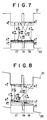
- Figs. 7 and 8 show energy bands in each coupled quantum well layer 15 of the light absorbing layer 11.
- e represents the energy level at a conduction band 21
- h and l respectively represent energy levels at a valence electron band 22.
- a superscript affix W attached to each of energy level characters designates the thicker quantum well layer 17, while a superscript affix N designates the thinner quantum well layer 18.
- a character E represents transition energy between the conduction band 21 and the valence electron band 22, and superscripts of E designate the quantum well layers in relation to the conduction band 21 and the valence electron band 22 in this order. With respect to energy transmitting in the same quantum well layer, only one superscript designating the corresponding quantum well layer is attached to the character E. Subscripts of transition energy E designate the quantum level of the conduction band 21 and that of the valence electron band 22. For instance, E 11h NW represents a transition energy E between an energy level e1 N at the conduction band 21 and an energy level h1 W at the valence electron band 22.
- the energy bands in each coupled quantum well layer 15 are bent in a thermal equilibrium state, as illustrated in Fig. 8. If light is introduced into this optical device as shown in Fig. 5, the built-in potential of the coupled quantum well layer 15 is screened by carriers excited by the light, thereby making the energy bands in each coupled quantum well layer 15 flat. Since the amount of carriers excited in each coupled quantum well layer 15 is proportional to the intensity of introduced light, the degree of flatness of the energy bands in each coupled quantum well layer 15 becomes higher as the intensity of light is increased, so that the state where the energy bands becomes closer to the completely flat state shown in Fig. 7. Therefore, during the transition from the state shown. in Fig. 8 to the state shown in Fig. 7, transposition of the energy levels e1 N and e1 W in the quantum well layers 17 and 18 at the conduction band 21 takes place.
- Figs. 9 and 10 show characteristics of absorbed peak energy with respect to the optical excitation intensity or the intensity of introduced light.
- transition energies E 11h, l W and EE 11h, l NW shown in Fig. 9 it is considered that the levels of these transition energies change and intersect each other, as indicated by the broken lines in Fig. 9, if the degree of coupling between the quantum well layers 17 and 18 is negligible. In this embodiment's optical element, however, the degree of coupling between the quantum well layers 17 and 18 is sufficiently high since these layers are formed on both surfaces of the tunnel barrier layer 19 having a small thickness of about 10 ⁇ .
- the transition energies EE 11h, l W and E 11h, l NW therefore change repulsively in the vicinity of the assumed point of intersection.
- transition energies or absorbed peak energies change in response to the optical excitation intensity, as indicated by the solid lines in Fig. 9.
- changes of the transition energies EE 11h, l WN and EE 11h, l N are illustrated in Fig. 10.
- signal light having a wavelength and an intensity such as to generate transition energy levels indicated by the solid lines in Figs. 9 and 10 is prepared, and this light is introduced into the optical element, as shown in Fig. 5.
- a control light different from the signal light is introduced into the optical element.
- the optical excitation intensity in each coupled quantum well layer 15 of the light absorbing layer 11 is changed to an extent corresponding to the intensity of the control light, and the absorbed peak energy is thereby abruptly changed. That is, the transmittance of the optical element with respect to the signal light is changed, thus enabling switching of the signal light.
- the energy bands in the light absorbing layer 11 are changed by the incidence of the control light.
- it is also possible to change the energy bands by providing the optical element with electrodes and forming an electric field, as in the case of the above-described conventional element.
- the optical element exhibits, with respect to signal light having a wavelength ⁇ 1 shown in Fig. 9, a transmittance characteristic, such as that shown in Fig. 11, which is generally symmetric about a light intensity I1, but it exhibits, with respect to signal light having a wavelength ⁇ 2 shown in Fig. 9, a transmittance characteristic, such as that shown in Fig. 12, in which the transmittance is minimized at a light intensity I2.
- the transmittance with respect to signal light having a wavelength ⁇ 3 shown in Fig. 9 is minimized at a light intensity I3, as shown in Fig. 13.
- the transmission characteristics or absorption characteristics of the optical element can be varied by only the wavelength of signal light.
- the thickness of the tunnel barrier layer 19 is set to a value not larger than 50 ⁇ in order to make the coupling between the quantum well layers 17 and 18 in the coupled quantum well layer 15 suitable.
- the signal light is introduced perpendicularly into the light absorbing layer 11, as shown in Fig. 5.
- the light absorbing layer 11 may be used as an optical waveguide into which the signal light is introduced in parallel therewith.
- a pair of quantum well layers 17 and 18 formed of the same material (GaAs) while having different thicknesses are used to form the coupled quantum well layer 15.
- the structure of this layer is not limited to this; a pair of quantum well layers having the same thickness and formed of different materials or a pair of quantum well layers having different thicknesses and formed of different materials may be used.
- the structure of the coupled quantum well layer 15 is limited to an asymmetric quantum well structure but a symmetric quantum well structure enables the same effects.
- the coupled quantum well layer 15 may have a multiple quantum well structure constituted by triple or more multiplicate lamination instead of the double quantum well structure.
Landscapes
- Physics & Mathematics (AREA)
- Nonlinear Science (AREA)
- Optics & Photonics (AREA)
- General Physics & Mathematics (AREA)
- Chemical & Material Sciences (AREA)
- Engineering & Computer Science (AREA)
- Nanotechnology (AREA)
- Crystallography & Structural Chemistry (AREA)
- Biophysics (AREA)
- Life Sciences & Earth Sciences (AREA)
- Photo Coupler, Interrupter, Optical-To-Optical Conversion Devices (AREA)
- Light Receiving Elements (AREA)
- Semiconductor Lasers (AREA)
Claims (11)
- Optisches Element zur Modulation von Licht, das folgendes aufweist:- eine Mantelschicht (12) vom p-Typ;- eine Mantelschicht (13) vom n-Typ; und- eine Lichtabsorptionseinrichtung (11), die zwischen den Mantelschichten (12, 13) vom p-Typ und vom n-Typ vorgesehen ist, wobei die Absorptionseinrichtung (11) wenigstens eine Quantenmulden-Vielfachlaminatstruktur hat, die ein Paar von Quantenmuldenschichten (17, 18) und eine erste Sperrschicht (19) zwischen diesem Paar von Quantenmuldenschichten (17, 18) aufweist;- wobei die erste Sperrschicht (19) eine Tunnelsperrschicht ist, so daß die Quantenmulden-Vielfachlaminatstruktur eine gekoppelte Quantenmulden-Vielfachlaminatstruktur (15) ist,dadurch gekennzeichnet,
daß die erste Sperrschicht (19) eine Dicke von nicht mehr als 50 Å hat und die gekoppelte Quantenmulden-Vielfachlaminatstruktur eine asymmetrische Quantenmulden-Laminatstruktur ist. - Optisches Element nach Anspruch 1,
wobei die Lichtabsorptionseinrichtung (11) eine Vielzahl von gekoppelten Quantenmulden-Vielfachlaminatstrukturen aufweist, die miteinander unter Zwischenfügung von zweiten Sperrschichten (16) laminiert sind. - Optisches Element nach einem der vorhergehenden Ansprüche, wobei die Mantelschicht (12) vom p-Typ, die Mantelschicht (13) vom n-Typ und die erste Sperrschicht (19) aus AlGaAs gebildet sind und das Paar von Quantenmuldenschichten (17, 18) aus GaAs gebildet ist.
- Optisches Element nach Anspruch 2 oder 3,
wobei die zweiten Sperrschichten (16) aus AlGaAs gebildet sind. - Optisches Element nach einem der vorhergehenden Ansprüche, das ferner ein Substrat (14) aufweist, das mit einer von der Mantelschicht (12) vom p-Typ und der Mantelschicht (13) vom n-Typ verbunden ist.
- Optisches Element nach Anspruch 5,
wobei das Substrat (14) aus GaAs gebildet ist. - Verfahren zum Modulieren von Signallicht, das folgendes aufweist:- Einkoppeln des Signallichts in ein optisches Element nach Anspruch 1; und- Veranlassen, daß die Quantenniveaus der Quantenmuldenschichten (17, 18) der gekoppelten Quantenmulden-Vielfachlaminatstruktur (15) einander durchdringen, so daß dadurch die Absorptionscharakteristiken der Lichtabsorptionseinrichtung (11) geändert werden, um das Signallicht zu modulieren.
- Verfahren nach Anspruch 7,
wobei die Durchdringung zwischen den Quantenniveaus der Quantenmuldenschichten durch Träger bewirkt wird, die in der Lichtabsorptionseinrichtung (11) erzeugt werden, wenn Steuerlicht, das von dem Signallicht verschieden ist, in das optische Element eingekoppelt wird. - Verfahren nach Anspruch 7,
wobei die Durchdringung zwischen den Quantenniveaus der Quantenmuldenschichten (17, 18) durch Träger bewirkt wird, die in der Lichtabsorptionseinrichtung (11) erzeugt werden, wenn das Signallicht in das optische Element eingekoppelt wird. - Verfahren nach Anspruch 7, 8 oder 9,
wobei das Signallicht in die Quantenmuldenschichten senkrecht dazu eingekoppelt wird. - Verfahren nach Anspruch 7, 8 oder 9,
wobei das Signallicht in die Quantenmuldenschichten parallel dazu eingekoppelt wird.
Applications Claiming Priority (4)
| Application Number | Priority Date | Filing Date | Title |
|---|---|---|---|
| JP21698888A JPH0263024A (ja) | 1988-08-30 | 1988-08-30 | 光素子 |
| JP216988/88 | 1988-08-30 | ||
| JP239416/88 | 1988-09-22 | ||
| JP63239416A JP2658266B2 (ja) | 1988-09-22 | 1988-09-22 | 光学的非線型素子 |
Publications (3)
| Publication Number | Publication Date |
|---|---|
| EP0361651A2 EP0361651A2 (de) | 1990-04-04 |
| EP0361651A3 EP0361651A3 (de) | 1991-04-10 |
| EP0361651B1 true EP0361651B1 (de) | 1995-12-06 |
Family
ID=26521747
Family Applications (1)
| Application Number | Title | Priority Date | Filing Date |
|---|---|---|---|
| EP89307331A Expired - Lifetime EP0361651B1 (de) | 1988-08-30 | 1989-07-19 | Optisches Element und Verfahren zum Modulieren von Licht unter Verwendung desselben |
Country Status (2)
| Country | Link |
|---|---|
| EP (1) | EP0361651B1 (de) |
| DE (1) | DE68925019T2 (de) |
Families Citing this family (2)
| Publication number | Priority date | Publication date | Assignee | Title |
|---|---|---|---|---|
| JPH03293622A (ja) * | 1990-04-12 | 1991-12-25 | Hitachi Ltd | 光変調器 |
| FR2728578A1 (fr) * | 1994-12-26 | 1996-06-28 | Inst Francais Du Petrole | Procede de vapocraquage flexible et installation de vapocraquage correspondante |
Citations (1)
| Publication number | Priority date | Publication date | Assignee | Title |
|---|---|---|---|---|
| WO1989009425A2 (en) * | 1988-03-24 | 1989-10-05 | Martin Marietta Corporation | Electro-optic quantum well device |
Family Cites Families (2)
| Publication number | Priority date | Publication date | Assignee | Title |
|---|---|---|---|---|
| US4626075A (en) * | 1983-01-03 | 1986-12-02 | At&T Bell Laboratories | Light beam applied to a layered semiconductor structure is controlled by another light beam |
| US4528464A (en) * | 1983-02-28 | 1985-07-09 | At&T Bell Laboratories | Degenerate four-wave mixer using multiple quantum well structures |
-
1989
- 1989-07-19 EP EP89307331A patent/EP0361651B1/de not_active Expired - Lifetime
- 1989-07-19 DE DE68925019T patent/DE68925019T2/de not_active Expired - Fee Related
Patent Citations (1)
| Publication number | Priority date | Publication date | Assignee | Title |
|---|---|---|---|---|
| WO1989009425A2 (en) * | 1988-03-24 | 1989-10-05 | Martin Marietta Corporation | Electro-optic quantum well device |
Non-Patent Citations (1)
| Title |
|---|
| Applied physics letter, vol. 49, no. 13, pp. 821-823 * |
Also Published As
| Publication number | Publication date |
|---|---|
| DE68925019D1 (de) | 1996-01-18 |
| EP0361651A2 (de) | 1990-04-04 |
| DE68925019T2 (de) | 1996-08-22 |
| EP0361651A3 (de) | 1991-04-10 |
Similar Documents
| Publication | Publication Date | Title |
|---|---|---|
| JP2955986B2 (ja) | 半導体光変調器及びその製造方法 | |
| JPH08220496A (ja) | 半導体光変調素子 | |
| JP2002268105A (ja) | 集積光スイッチングデバイスおよび光をスイッチングする方法 | |
| JPH0422254B2 (de) | ||
| JPH08146365A (ja) | 半導体マッハツェンダー変調装置及びその製造方法 | |
| US5621564A (en) | Semiconductor optical modulator | |
| EP0361651B1 (de) | Optisches Element und Verfahren zum Modulieren von Licht unter Verwendung desselben | |
| JP3006553B2 (ja) | 半導体集積型偏波モード変換器 | |
| JPS61212823A (ja) | 光変調器 | |
| JPH09288288A (ja) | 光機能素子 | |
| JP2760276B2 (ja) | 選択成長導波型光制御素子 | |
| JP3490510B2 (ja) | 光半導体装置 | |
| JP4121409B2 (ja) | 光出力装置 | |
| JP2940238B2 (ja) | 光スイッチ | |
| JP4738627B2 (ja) | 面型光−光スイッチ | |
| JP2730466B2 (ja) | 光スイッチ | |
| JPH0263024A (ja) | 光素子 | |
| JPH11109298A (ja) | 半導体素子 | |
| JP3076251B2 (ja) | 光機能素子及びそれを用いた光スイッチ | |
| JPH04291982A (ja) | 光変調器 | |
| JPH0695182A (ja) | 光スイッチ | |
| JPH11142799A (ja) | 光変調器 | |
| JPH0667222A (ja) | 導波路形光スイッチ | |
| JPH03119328A (ja) | 半導体積層構造 | |
| JPH04291316A (ja) | 屈折率変調型光変調器 |
Legal Events
| Date | Code | Title | Description |
|---|---|---|---|
| PUAI | Public reference made under article 153(3) epc to a published international application that has entered the european phase |
Free format text: ORIGINAL CODE: 0009012 |
|
| AK | Designated contracting states |
Kind code of ref document: A2 Designated state(s): DE GB NL |
|
| 17P | Request for examination filed |
Effective date: 19901210 |
|
| PUAL | Search report despatched |
Free format text: ORIGINAL CODE: 0009013 |
|
| AK | Designated contracting states |
Kind code of ref document: A3 Designated state(s): DE GB NL |
|
| 17Q | First examination report despatched |
Effective date: 19930923 |
|
| GRAA | (expected) grant |
Free format text: ORIGINAL CODE: 0009210 |
|
| AK | Designated contracting states |
Kind code of ref document: B1 Designated state(s): DE GB NL |
|
| REF | Corresponds to: |
Ref document number: 68925019 Country of ref document: DE Date of ref document: 19960118 |
|
| REG | Reference to a national code |
Ref country code: GB Ref legal event code: 727 |
|
| REG | Reference to a national code |
Ref country code: GB Ref legal event code: 727A |
|
| REG | Reference to a national code |
Ref country code: GB Ref legal event code: 727B |
|
| REG | Reference to a national code |
Ref country code: GB Ref legal event code: SP |
|
| PLBE | No opposition filed within time limit |
Free format text: ORIGINAL CODE: 0009261 |
|
| STAA | Information on the status of an ep patent application or granted ep patent |
Free format text: STATUS: NO OPPOSITION FILED WITHIN TIME LIMIT |
|
| 26N | No opposition filed | ||
| REG | Reference to a national code |
Ref country code: GB Ref legal event code: 746 Effective date: 19971202 |
|
| PGFP | Annual fee paid to national office [announced via postgrant information from national office to epo] |
Ref country code: GB Payment date: 20010718 Year of fee payment: 13 |
|
| REG | Reference to a national code |
Ref country code: GB Ref legal event code: IF02 |
|
| PG25 | Lapsed in a contracting state [announced via postgrant information from national office to epo] |
Ref country code: GB Free format text: LAPSE BECAUSE OF NON-PAYMENT OF DUE FEES Effective date: 20020719 |
|
| PGFP | Annual fee paid to national office [announced via postgrant information from national office to epo] |
Ref country code: DE Payment date: 20020724 Year of fee payment: 14 |
|
| PGFP | Annual fee paid to national office [announced via postgrant information from national office to epo] |
Ref country code: NL Payment date: 20020730 Year of fee payment: 14 |
|
| GBPC | Gb: european patent ceased through non-payment of renewal fee |
Effective date: 20020719 |
|
| PG25 | Lapsed in a contracting state [announced via postgrant information from national office to epo] |
Ref country code: NL Free format text: LAPSE BECAUSE OF NON-PAYMENT OF DUE FEES Effective date: 20040201 |
|
| PG25 | Lapsed in a contracting state [announced via postgrant information from national office to epo] |
Ref country code: DE Free format text: LAPSE BECAUSE OF NON-PAYMENT OF DUE FEES Effective date: 20040203 |
|
| NLV4 | Nl: lapsed or anulled due to non-payment of the annual fee |
Effective date: 20040201 |