EP0361742A2 - Optische Bauelemente - Google Patents
Optische Bauelemente Download PDFInfo
- Publication number
- EP0361742A2 EP0361742A2 EP89309384A EP89309384A EP0361742A2 EP 0361742 A2 EP0361742 A2 EP 0361742A2 EP 89309384 A EP89309384 A EP 89309384A EP 89309384 A EP89309384 A EP 89309384A EP 0361742 A2 EP0361742 A2 EP 0361742A2
- Authority
- EP
- European Patent Office
- Prior art keywords
- waveguide
- optical device
- width
- matching region
- laser diode
- Prior art date
- Legal status (The legal status is an assumption and is not a legal conclusion. Google has not performed a legal analysis and makes no representation as to the accuracy of the status listed.)
- Withdrawn
Links
Images
Classifications
-
- G—PHYSICS
- G02—OPTICS
- G02B—OPTICAL ELEMENTS, SYSTEMS OR APPARATUS
- G02B6/00—Light guides; Structural details of arrangements comprising light guides and other optical elements, e.g. couplings
- G02B6/24—Coupling light guides
- G02B6/42—Coupling light guides with opto-electronic elements
- G02B6/4201—Packages, e.g. shape, construction, internal or external details
- G02B6/4202—Packages, e.g. shape, construction, internal or external details for coupling an active element with fibres without intermediate optical elements, e.g. fibres with plane ends, fibres with shaped ends, bundles
- G02B6/4203—Optical features
-
- G—PHYSICS
- G02—OPTICS
- G02B—OPTICAL ELEMENTS, SYSTEMS OR APPARATUS
- G02B6/00—Light guides; Structural details of arrangements comprising light guides and other optical elements, e.g. couplings
- G02B6/24—Coupling light guides
- G02B6/42—Coupling light guides with opto-electronic elements
Definitions
- This invention relates to optical devices and more particularly, but not exclusively, to a device which includes matching of a diode laser to a monomode optical waveguide.
- the present invention seeks to provide improved matching between a laser diode and a waveguide.
- an optical device comprises a laser diode, an optical waveguide, and a matching region between and adjacent to them having a width in one plane which increases from a first part adjacent to the laser diode to a second part of greatest width and decreases from the second part to a third part of smaller width adjacent to the waveguide.
- a significant amount of light radiating at high angles from the laser diode may be collected and then guided into a narrower waveguide.
- the boundaries of the matching region are smoothly curved in the plane in which its width changes.
- the width of the matching region at the third part is greater than that at the first part, although if the waveguide is narrower than the laser diode output aperture the width at the third part may be smaller.
- the waveguide may be monomode at the laser operating frequency and the matching region may be such that its part of greater width is capable of sustaining more than a single waveguide mode.
- the greatest width of the matching region is less than three times the width of the waveguide.
- the matching region has approximately the same refractive index as the waveguide, giving similar optical characteristics and conveniently, the waveguide and the matching region are fabricated by the same process.
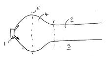
- a "bulbous" matching region 4 is located between the laser 1 and waveguide 2 and has smoothly curving edges. At its greatest width, indicated by broken line 5, the section 4 is about twice the width of the monomode waveguide 2. Light emitted at wide angles, as illustrated by the arrows, from the laser 1 tends to be confined within the guide 4 and channelled into the monomode waveguide 2.
- the waveguide 2 and matching region 4 have the same refractive index and are fabricated by the same process.
Landscapes
- Physics & Mathematics (AREA)
- General Physics & Mathematics (AREA)
- Optics & Photonics (AREA)
- Semiconductor Lasers (AREA)
- Optical Integrated Circuits (AREA)
Applications Claiming Priority (2)
| Application Number | Priority Date | Filing Date | Title |
|---|---|---|---|
| GB888823010A GB8823010D0 (en) | 1988-09-30 | 1988-09-30 | Matching arrangement |
| GB8823010 | 1988-09-30 |
Publications (2)
| Publication Number | Publication Date |
|---|---|
| EP0361742A2 true EP0361742A2 (de) | 1990-04-04 |
| EP0361742A3 EP0361742A3 (de) | 1990-10-24 |
Family
ID=10644537
Family Applications (1)
| Application Number | Title | Priority Date | Filing Date |
|---|---|---|---|
| EP19890309384 Withdrawn EP0361742A3 (de) | 1988-09-30 | 1989-09-15 | Optische Bauelemente |
Country Status (2)
| Country | Link |
|---|---|
| EP (1) | EP0361742A3 (de) |
| GB (2) | GB8823010D0 (de) |
Cited By (1)
| Publication number | Priority date | Publication date | Assignee | Title |
|---|---|---|---|---|
| US6957904B2 (en) | 2001-07-30 | 2005-10-25 | 3M Innovative Properties Company | Illumination device utilizing displaced radiation patterns |
Family Cites Families (7)
| Publication number | Priority date | Publication date | Assignee | Title |
|---|---|---|---|---|
| DE2363253A1 (de) * | 1973-12-19 | 1975-06-26 | Siemens Ag | Koppelvorrichtung und verfahren zu deren herstellung |
| AU510340B2 (en) * | 1977-11-28 | 1980-06-19 | Deutsch Co. Electronics Components Division, The | Optical interconnecting device |
| US4257672A (en) * | 1978-12-28 | 1981-03-24 | International Business Machines Corporation | Optical coupler for connecting a light source to an optical transmission line |
| US4666236A (en) * | 1982-08-10 | 1987-05-19 | Omron Tateisi Electronics Co. | Optical coupling device and method of producing same |
| EP0220455A1 (de) * | 1985-09-24 | 1987-05-06 | Siemens Aktiengesellschaft | Anordnung zur Kopplung einer Laserdiode und eines Monomode-Lichtwellenleiters |
| EP0246793A3 (de) * | 1986-05-19 | 1988-06-01 | AT&T Corp. | Hochleistungslaser mit fundamentaler transversaler Mode |
| US4826272A (en) * | 1987-08-27 | 1989-05-02 | American Telephone And Telegraph Company At&T Bell Laboratories | Means for coupling an optical fiber to an opto-electronic device |
-
1988
- 1988-09-30 GB GB888823010A patent/GB8823010D0/en active Pending
-
1989
- 1989-09-12 GB GB8920646A patent/GB2223327B/en not_active Expired - Lifetime
- 1989-09-15 EP EP19890309384 patent/EP0361742A3/de not_active Withdrawn
Cited By (1)
| Publication number | Priority date | Publication date | Assignee | Title |
|---|---|---|---|---|
| US6957904B2 (en) | 2001-07-30 | 2005-10-25 | 3M Innovative Properties Company | Illumination device utilizing displaced radiation patterns |
Also Published As
| Publication number | Publication date |
|---|---|
| GB2223327B (en) | 1992-09-16 |
| GB8920646D0 (en) | 1989-10-25 |
| GB8823010D0 (en) | 1988-11-09 |
| EP0361742A3 (de) | 1990-10-24 |
| GB2223327A (en) | 1990-04-04 |
Similar Documents
| Publication | Publication Date | Title |
|---|---|---|
| US5033812A (en) | Grating coupler | |
| US6980720B2 (en) | Mode transformation and loss reduction in silicon waveguide structures utilizing tapered transition regions | |
| US4351585A (en) | Coupling element for an optical waveguide | |
| US4678267A (en) | Parabolic optical waveguide horns and design thereof | |
| EP0301194A2 (de) | Sternkoppler | |
| CA2028328A1 (en) | Optical divider for multimode optical fiber systems | |
| EP0385671A3 (de) | Verlustarme Wellenleiterkreuzung | |
| CA2004046A1 (en) | Integrated optic print head | |
| JP2002539616A (ja) | 側面ポンプ・ファイバ・レーザ | |
| EP0361742A2 (de) | Optische Bauelemente | |
| JPH08160233A (ja) | 集積光学素子 | |
| US4988156A (en) | Bent waveguide for an optical integrated circuit | |
| US4278322A (en) | Coupling device for coupling of two waveguides | |
| JPH08122547A (ja) | 非対称y分岐導波路型光タップ | |
| RU2000103857A (ru) | Способ изготовления волноводов интегрально-оптической схемы волоконно-оптического гироскопа | |
| DE60233332D1 (de) | Array-wellenleitergitter mit verringerter chromatischer dispersion | |
| EP0397895A1 (de) | Verfahren zur Herstellung von Linsen in flachen optischen Monomodeleitern aus LiNbO3 | |
| JPS5559402A (en) | Photo switch | |
| JPS5788410A (en) | Cross waveguide and optical switch | |
| JPH0361924B2 (de) | ||
| JPS57150814A (en) | Optical distributing circuit | |
| JP2819175B2 (ja) | 導波路型光減衰器および光集積回路 | |
| JPS6069608A (ja) | 光分岐装置 | |
| JPS649679A (en) | Semiconductor laser of long resonator length | |
| JP2004318159A (ja) | 改良型反射鏡の特徴をもつ導波構造 |
Legal Events
| Date | Code | Title | Description |
|---|---|---|---|
| PUAI | Public reference made under article 153(3) epc to a published international application that has entered the european phase |
Free format text: ORIGINAL CODE: 0009012 |
|
| AK | Designated contracting states |
Kind code of ref document: A2 Designated state(s): DE FR IT |
|
| PUAL | Search report despatched |
Free format text: ORIGINAL CODE: 0009013 |
|
| AK | Designated contracting states |
Kind code of ref document: A3 Designated state(s): DE FR IT |
|
| 17P | Request for examination filed |
Effective date: 19910411 |
|
| 17Q | First examination report despatched |
Effective date: 19920519 |
|
| STAA | Information on the status of an ep patent application or granted ep patent |
Free format text: STATUS: THE APPLICATION IS DEEMED TO BE WITHDRAWN |
|
| 18D | Application deemed to be withdrawn |
Effective date: 19930504 |