EP0361782B1 - Dispositif électro-optique - Google Patents
Dispositif électro-optique Download PDFInfo
- Publication number
- EP0361782B1 EP0361782B1 EP89309591A EP89309591A EP0361782B1 EP 0361782 B1 EP0361782 B1 EP 0361782B1 EP 89309591 A EP89309591 A EP 89309591A EP 89309591 A EP89309591 A EP 89309591A EP 0361782 B1 EP0361782 B1 EP 0361782B1
- Authority
- EP
- European Patent Office
- Prior art keywords
- electrode
- travelling wave
- potentials
- ground plane
- electro
- Prior art date
- Legal status (The legal status is an assumption and is not a legal conclusion. Google has not performed a legal analysis and makes no representation as to the accuracy of the status listed.)
- Expired - Lifetime
Links
- GQYHUHYESMUTHG-UHFFFAOYSA-N lithium niobate Chemical compound [Li+].[O-][Nb](=O)=O GQYHUHYESMUTHG-UHFFFAOYSA-N 0.000 claims description 10
- 239000000463 material Substances 0.000 claims description 8
- 238000000034 method Methods 0.000 claims description 3
- 230000005540 biological transmission Effects 0.000 abstract description 5
- 230000005684 electric field Effects 0.000 description 5
- 239000003990 capacitor Substances 0.000 description 4
- 230000000694 effects Effects 0.000 description 4
- 230000003287 optical effect Effects 0.000 description 3
- 239000013307 optical fiber Substances 0.000 description 3
- 230000008901 benefit Effects 0.000 description 2
- 230000008859 change Effects 0.000 description 2
- 230000009467 reduction Effects 0.000 description 2
- RTAQQCXQSZGOHL-UHFFFAOYSA-N Titanium Chemical compound [Ti] RTAQQCXQSZGOHL-UHFFFAOYSA-N 0.000 description 1
- 238000004891 communication Methods 0.000 description 1
- 230000008878 coupling Effects 0.000 description 1
- 238000010168 coupling process Methods 0.000 description 1
- 238000005859 coupling reaction Methods 0.000 description 1
- 230000001066 destructive effect Effects 0.000 description 1
- 230000007613 environmental effect Effects 0.000 description 1
- 239000000382 optic material Substances 0.000 description 1
- 230000000737 periodic effect Effects 0.000 description 1
- 230000004044 response Effects 0.000 description 1
- 239000000758 substrate Substances 0.000 description 1
- 230000002277 temperature effect Effects 0.000 description 1
- 229910052719 titanium Inorganic materials 0.000 description 1
- 239000010936 titanium Substances 0.000 description 1
Images

Classifications
-
- G—PHYSICS
- G02—OPTICS
- G02F—OPTICAL DEVICES OR ARRANGEMENTS FOR THE CONTROL OF LIGHT BY MODIFICATION OF THE OPTICAL PROPERTIES OF THE MEDIA OF THE ELEMENTS INVOLVED THEREIN; NON-LINEAR OPTICS; FREQUENCY-CHANGING OF LIGHT; OPTICAL LOGIC ELEMENTS; OPTICAL ANALOGUE/DIGITAL CONVERTERS
- G02F1/00—Devices or arrangements for the control of the intensity, colour, phase, polarisation or direction of light arriving from an independent light source, e.g. switching, gating or modulating; Non-linear optics
- G02F1/01—Devices or arrangements for the control of the intensity, colour, phase, polarisation or direction of light arriving from an independent light source, e.g. switching, gating or modulating; Non-linear optics for the control of the intensity, phase, polarisation or colour
- G02F1/21—Devices or arrangements for the control of the intensity, colour, phase, polarisation or direction of light arriving from an independent light source, e.g. switching, gating or modulating; Non-linear optics for the control of the intensity, phase, polarisation or colour by interference
- G02F1/225—Devices or arrangements for the control of the intensity, colour, phase, polarisation or direction of light arriving from an independent light source, e.g. switching, gating or modulating; Non-linear optics for the control of the intensity, phase, polarisation or colour by interference in an optical waveguide structure
- G02F1/2255—Devices or arrangements for the control of the intensity, colour, phase, polarisation or direction of light arriving from an independent light source, e.g. switching, gating or modulating; Non-linear optics for the control of the intensity, phase, polarisation or colour by interference in an optical waveguide structure controlled by a high-frequency electromagnetic component in an electric waveguide structure
-
- G—PHYSICS
- G02—OPTICS
- G02F—OPTICAL DEVICES OR ARRANGEMENTS FOR THE CONTROL OF LIGHT BY MODIFICATION OF THE OPTICAL PROPERTIES OF THE MEDIA OF THE ELEMENTS INVOLVED THEREIN; NON-LINEAR OPTICS; FREQUENCY-CHANGING OF LIGHT; OPTICAL LOGIC ELEMENTS; OPTICAL ANALOGUE/DIGITAL CONVERTERS
- G02F1/00—Devices or arrangements for the control of the intensity, colour, phase, polarisation or direction of light arriving from an independent light source, e.g. switching, gating or modulating; Non-linear optics
- G02F1/29—Devices or arrangements for the control of the intensity, colour, phase, polarisation or direction of light arriving from an independent light source, e.g. switching, gating or modulating; Non-linear optics for the control of the position or the direction of light beams, i.e. deflection
- G02F1/31—Digital deflection, i.e. optical switching
- G02F1/313—Digital deflection, i.e. optical switching in an optical waveguide structure
- G02F1/3132—Digital deflection, i.e. optical switching in an optical waveguide structure of directional coupler type
- G02F1/3134—Digital deflection, i.e. optical switching in an optical waveguide structure of directional coupler type controlled by a high-frequency electromagnetic wave component in an electric waveguide structure
Definitions
- This invention relates to electro-optic waveguide devices and in particular to interferometers and directional couplers having travelling-wave electrodes.
- Electro-optic materials such as lithium niobate (LNB) and KTP, have refractive indices which vary according to the magnitude and direction of applied electric field.
- Waveguide devices based on such materials are potentially useful for optical fibre communication and signal processing systems. Typically such devices are required to operate with light of wavelengths in the range 0.6 to 1.6»m, and in particular with light in the range 1.3 to 1.6»m.
- MZ interferometers There are two basic device types: directional couplers; and Mach-Zehnder (MZ) interferometers. The first of these utilises the electro-optic effect to control the coupling between a pair of adjacent waveguides. By controlling their refractive indices it is possible to couple light from one waveguide to the other or vice versa.
- MZ interferometer an input waveguide is coupled to an output waveguide by a pair of waveguide arms. Each arm has an associated electrode by means of which it is possible to control the refractive indices of, and hence the velocity of propagation in, the two arms independently. It is therefore possible, by controlling the applied electric fields, to produce phase differences between signals travelling in the two arms resulting in constructive or destructive interference when they are combined. Thus it is possible to amplitude modulate input optical signals according to the voltage difference between the electrodes.
- materials such as LNB which exhibit the electro-optic effect tend also to be pyroelectric: electric fields are produced within the material as the result of a temperature change.
- the pyroelectric effect is so strong that a temperature change of a degree or less may be sufficient to produce an electric field comparable to that applied to produce switching of states in a directional coupler or MZ interferometer made of the material.
- Such electric fields strongly affect the optical states of the devices. Consequently it is necessary, with materials such as z-cut LNB which exhibit a strong pyroelectric effect, to provide very precise temperature control if reliable and repeatable performance is to be achieved from electro-optic waveguide devices based on such materials.
- thermally-induced instabilities may remain in devices in which there is power dissipation in the electrodes.
- Examples of devices with power dissipating electrodes include directional couplers and MZ interferometers having travelling-wave electrodes.
- the use of travelling-wave electrodes potentially enables the production of devices capable of very high speed operation (typically switchable at gigabit rates).
- a further advantage of such devices is that they offer a very large bandwidth, typically from dc to 4GHz.
- the travelling-wave electrode is part of a transmission line and has finite resistance, non-zero signal levels cause power to be dissipated in the electrode, thus raising the temperature of the underlying waveguide.
- the stability of these devices is jeopardised if there is in the electrical signal applied to the electrodes a low frequency component having a period longer than the thermal response time of the electrodes (of the order of 0.1 second) as such components cause variations in power dissipation and hence temperature fluctuations.
- This power variation can shift the transfer characteristic by as much as 3 volts or more which, the switching voltage being in the range 3.5 to 4.0 volts, makes the device unusable.
- the present invention provides apparatus comprising an electro-optic waveguide device having a travelling wave electrode structure including a travelling wave electrode and a ground plane electrode, the device being switchable between first and second distinct states by the application of respective first and second potentials to the travelling wave electrode; and means for supplying said first and second potentials to said travelling wave electrode, characterised in that the apparatus further comprises means to bias said ground plane electrode such that said first and second potentials are of substantially equal magnitude but of opposite sign.
- the present invention provides a method of driving an electro-optic device having a power dissipating electrode structure comprising a power dissipating electrode and a ground plane electrode, the device being switchable between first and second distinct states by application of respective first and second potentials to the power dissipating electrode, characterised in that a bias voltage is applied to the ground plane electrode such that the magnitude of the current carried by the power dissipating electrode is substantially the same in each of said first and second states.
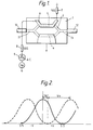
- FIG. 1 a typical travelling-wave electrode Mach-Zehnder interferometer is shown.
- the device is formed on a Z-cut lithium niobate (LNB) substrate 1, typically 40mm long, 10mm wide and 1mm thick, and comprises a waveguide structure 2 formed by diffusing titanium into the LNB.
- a ground plane electrode overlies one of the interferometer arms 4 and is connected directly to ground.
- Over the other interferometer arm 5 there extends a travelling-wave electrode 6.
- One end of the travelling-wave electrode 6 is connected via a 50ohm transmission line termination 7 to ground.
- the other end of the travelling-wave electrode is connected via a 50ohm transmission line 8 to the modulating voltage source 9 the other pole of which is connected to ground.
- Optical input signals are supplied to the interferometer by an optical fibre 10 which is aligned with the waveguide input portion 11.
- the interferometer output is fed into a second optical fibre 12 aligned with the waveguide output portion 13.
- FIG 2 shows the transfer function of an interferometer such as that shown in Figure 1.
- the transfer function is essentially of periodic cos squared type.
- the electrode potential that is the potential difference between the travelling-wave electrode and ground potential
- the electrode voltage required to drive the output from a peak to a trough is called the switching voltage V ⁇ .
- a typical switching voltage for 20mm long electrodes on Z-cut LNB is about 3.5V.
- the curve represented as a broken line corresponds to a typical transfer characteristic, where the light output null corresponds to a non-zero electrode potential.
- the voltage required to obtain the output null nearest to zero volts is the phase bias voltage Vo.
- the phase bias voltage can have any value up to the switching voltage and can vary widely from device to device, even when the devices are notionally identical.
- the worst case with regard to differences in power dissipation between the two switched states for any switching voltage occurs when the phase bias voltage Vo equals the switching voltage or is zero, as represented by the solid line curve in Figure 2.
- FIG 3 there is shown schematically a solution to the problem.
- the electrode driving arrangement is different to that employed conventionally and shown in Figure 1.
- the ground plane electrode is no longer connected directly to earth. Instead the ground plane electrode is connected to earth via a high frequency decoupling network, comprising a decoupling capacitor (e.g. 50nF) and a resistor (e.g.1K ) in parallel.
- a voltage source which provides a bias voltage which is used to offset the device transfer characteristic relative to zero volts.
- the device of Figure 3 has, like the device whose transfer characteristic appears as a solid line in Figure 2, a switching voltage V ⁇ of 3.5V.
- the transfer characteristic is shifted so that a peak output occurs for a travelling-wave electrode potential of -1.75 volts, while a trough output occurs for a travelling-wave electrode potential of +1.75 volts.
- the travelling-wave electrode has a finite resistance, there is a voltage drop throughout its length and this must be borne in mind when measuring and quoting travelling-wave electrode potentials. It is convenient to use either the mean average electrode voltage of the median (mid-point) electrode voltage.
- the magnitude of the potential applied to the travelling-wave electrode is the same for both switched states of the device, the magnitude of the current flowing through the travelling-wave electrode and consequently the power dissipation will be the same in both states.
- this arrangement has the added benefit that reductions in the worst-case direct current level in the travelling-wave electrode result in reduced electromigration with a consequent increase in electrode life.
- the 50% reduction in direct current level in the present example would be expected to increase electrode life by about four times.
- the necessary ground plane bias voltage can only be determined when the MZ interferometer is in thermal equilibrium, that is when the travelling wave electrode has been biased to V ⁇ /2 for a sufficient period for thermal equilibrium to have been reached.
Landscapes
- Physics & Mathematics (AREA)
- Nonlinear Science (AREA)
- General Physics & Mathematics (AREA)
- Optics & Photonics (AREA)
- Electromagnetism (AREA)
- Optical Modulation, Optical Deflection, Nonlinear Optics, Optical Demodulation, Optical Logic Elements (AREA)
- Optical Integrated Circuits (AREA)
- Tests Of Electronic Circuits (AREA)
- Measurement Of Current Or Voltage (AREA)
- Details Of Television Scanning (AREA)
- Liquid Crystal (AREA)
- Control Of El Displays (AREA)
- Control Of Indicators Other Than Cathode Ray Tubes (AREA)
Claims (7)
- Appareil comprenant un dispositif guide d'onde électro-optique ayant une structure d'électrode à onde progressive incorporant une électrode à onde progressive et une électrode en plan de masse, le dispositif pouvant être commuté entre des premier et second états distincts par application des premier et second potentiels respectifs à l'électrode d'onde progressive; et des moyens pour appliquer les premier et second potentiels à l'électrode d'onde progressive; caractérisé en ce que l'appareil comprend de plus des moyens pour polariser l'électrode de plan de masse pour que les premier et second potentiels soient d'une grandeur sensiblement égale mais de signe opposé.
- Appareil selon la revendication 1, comprenant de plus un réseau de découplage haute fréquence, connecté électriquement à l'électrode de plan de masse.
- Appareil comprenant un dispositif de guide d'onde électro-optique ayant une zone de guidage d'onde formée dans un matériau pyroélectrique, et une structure d'électrode d'onde progressive incluant une électrode d'onde progressive et une électrode de plan de masse, le dispositif pouvant être commuté entre les premier et second états distincts par application des premier et second potentiels respectifs à l'électrode d'onde progressive; et des moyens pour appliquer les premier et second potentiels à l'électrode d'onde progressive; caractérisé en ce que l'appareil comprend de plus des moyens pour polariser l'électrode de plan de masse pour que la grandeur du courant porté par l'électrode d'onde progressive soit sensiblement égale dans chacun des premier et second états.
- Appareil selon l'une quelconque des revendications précédentes, dans lequel le dispositif électro-optique est un interféromètre Mach-Zehnder ou un coupleur directionnel.
- Appareil selon l'une quelconque des revendications précédentes, dans lequel le dispositif électro-optique comprend du niobate de lithium.
- Procédé pour commander un dispositif de guide d'onde électro-optique ayant une structure d'électrode d'onde progressive incluant une électrode d'onde progressive et une électrode de plan de masse, dans lequel on applique une tension de polarisation à l'électrode de plan de masse et des premier et second potentiels de grandeur sensiblement égale mais de polarité opposée sont appliqués à l'électrode d'onde progressive pour permettre la commutation par la pleine tension de commutation Vπ vers et à partir du point de polarisation de phase.
- Procédé pour commander un dispositif électro-optique ayant une structure d'électrode de dissipation de puissance comprenant une électrode de dissipation de puissance et une électrode de plan de masse, le dispositif pouvant être commuté entre des premier et second états distincts par application des premier et second potentiels respectifs à l'électrode de dissipation de puissance, caractérisé en ce qu'une tension de polarisation est appliquée à l'électrode plan de masse de telle sorte que la grandeur du courant portée par l'électrode de dissipation de puissance est sensiblement la même dans chacun des premier et second états.
Applications Claiming Priority (2)
| Application Number | Priority Date | Filing Date | Title |
|---|---|---|---|
| GB888822288A GB8822288D0 (en) | 1988-09-22 | 1988-09-22 | Electro-optic device |
| GB8822288 | 1988-09-22 |
Publications (2)
| Publication Number | Publication Date |
|---|---|
| EP0361782A1 EP0361782A1 (fr) | 1990-04-04 |
| EP0361782B1 true EP0361782B1 (fr) | 1994-08-24 |
Family
ID=10644067
Family Applications (1)
| Application Number | Title | Priority Date | Filing Date |
|---|---|---|---|
| EP89309591A Expired - Lifetime EP0361782B1 (fr) | 1988-09-22 | 1989-09-20 | Dispositif électro-optique |
Country Status (9)
| Country | Link |
|---|---|
| US (1) | US5276744A (fr) |
| EP (1) | EP0361782B1 (fr) |
| JP (1) | JPH04501013A (fr) |
| KR (1) | KR900702401A (fr) |
| AT (1) | ATE110474T1 (fr) |
| CA (1) | CA1323920C (fr) |
| DE (1) | DE68917667D1 (fr) |
| GB (1) | GB8822288D0 (fr) |
| WO (1) | WO1990003594A1 (fr) |
Families Citing this family (4)
| Publication number | Priority date | Publication date | Assignee | Title |
|---|---|---|---|---|
| JP3742477B2 (ja) * | 1997-02-17 | 2006-02-01 | 富士通株式会社 | 光変調器 |
| US6372284B1 (en) | 1998-06-11 | 2002-04-16 | Optelecom, Inc. | Fluoropolymer coating of lithium niobate integrated optical devices |
| JP4789460B2 (ja) * | 2004-12-22 | 2011-10-12 | 株式会社アドバンテスト | 光スイッチ及び光試験装置 |
| JP6330549B2 (ja) * | 2014-07-25 | 2018-05-30 | 住友電気工業株式会社 | 光半導体素子およびその製造方法 |
Family Cites Families (10)
| Publication number | Priority date | Publication date | Assignee | Title |
|---|---|---|---|---|
| US4253734A (en) * | 1979-10-22 | 1981-03-03 | Mitsubishi Denki Kabushiki Kaisha | Electro optical modulation system |
| JPS57185418A (en) * | 1981-05-11 | 1982-11-15 | Nec Corp | Optical switching method |
| JPS5882223A (ja) * | 1981-11-11 | 1983-05-17 | Matsushita Electric Ind Co Ltd | 光シヤツタ−素子の駆動方法 |
| JPH0629919B2 (ja) * | 1982-04-16 | 1994-04-20 | 株式会社日立製作所 | 液晶素子の駆動方法 |
| US4703996A (en) * | 1984-08-24 | 1987-11-03 | American Telephone And Telegraph Company, At&T Bell Laboratories | Integrated optical device having integral photodetector |
| JPS6199122A (ja) * | 1984-10-22 | 1986-05-17 | Nec Corp | 半導体光スイツチの駆動方法 |
| US4903029A (en) * | 1988-03-18 | 1990-02-20 | Hughes Aircraft Company | Delayed replica radar test set target |
| US4936644A (en) * | 1989-06-13 | 1990-06-26 | Hoechst Celanese Corp. | Polarization-insensitive interferometric waveguide electrooptic modulator |
| US4936645A (en) * | 1989-08-24 | 1990-06-26 | Hoechst Celanese Corp. | Waveguide electrooptic light modulator with low optical loss |
| US5040865A (en) * | 1990-04-20 | 1991-08-20 | Hughes Aircraft Company | Frequency multiplying electro-optic modulator configuration and method |
-
1988
- 1988-09-22 GB GB888822288A patent/GB8822288D0/en active Pending
-
1989
- 1989-09-20 US US07/663,891 patent/US5276744A/en not_active Expired - Fee Related
- 1989-09-20 KR KR1019900701076A patent/KR900702401A/ko not_active Ceased
- 1989-09-20 WO PCT/GB1989/001099 patent/WO1990003594A1/fr not_active Ceased
- 1989-09-20 JP JP1510237A patent/JPH04501013A/ja active Pending
- 1989-09-20 AT AT89309591T patent/ATE110474T1/de active
- 1989-09-20 EP EP89309591A patent/EP0361782B1/fr not_active Expired - Lifetime
- 1989-09-20 DE DE68917667T patent/DE68917667D1/de not_active Expired - Lifetime
- 1989-09-21 CA CA000612428A patent/CA1323920C/fr not_active Expired - Fee Related
Non-Patent Citations (1)
| Title |
|---|
| A. Yariv, "QUANTUM ELECTRONICS", 2nd edition, J. Wiley & Sons, New York, 1975, pp. 339-341. * |
Also Published As
| Publication number | Publication date |
|---|---|
| EP0361782A1 (fr) | 1990-04-04 |
| ATE110474T1 (de) | 1994-09-15 |
| GB8822288D0 (en) | 1988-10-26 |
| US5276744A (en) | 1994-01-04 |
| KR900702401A (ko) | 1990-12-07 |
| DE68917667D1 (de) | 1994-09-29 |
| WO1990003594A1 (fr) | 1990-04-05 |
| JPH04501013A (ja) | 1992-02-20 |
| CA1323920C (fr) | 1993-11-02 |
Similar Documents
| Publication | Publication Date | Title |
|---|---|---|
| EP0674210B1 (fr) | Modulateur optique | |
| EP0444688B1 (fr) | Emetteur optique | |
| US5917628A (en) | Optical time-division multiplexer capable of supplying stable output signal | |
| CA2335430C (fr) | Modulation optique externe employant des circuits de compensation non co-lineaires | |
| CA1290435C (fr) | Dispositif modulateur de signaux optiques | |
| EP0427092B1 (fr) | Modulateur électro-optique | |
| JP2002350796A (ja) | マッハ−ツェンダ電子−光学変調器 | |
| JP2848942B2 (ja) | 光送信装置 | |
| JPS6378124A (ja) | 偏極調整装置 | |
| US4776656A (en) | TE-TM mode converter | |
| US6526186B2 (en) | Optical modulator having coplanar electrodes for controlling chirp | |
| US4842367A (en) | Optoelectronic directional coupler for a bias-free control signal | |
| US20030016430A1 (en) | LiNbO3 Mach-Zehnder modulator with low drive voltage requirement and adjustable chirp | |
| US6222965B1 (en) | Bias control system for electrooptic devices | |
| EP0361782B1 (fr) | Dispositif électro-optique | |
| JP4184131B2 (ja) | 光ssb変調装置 | |
| WO1985001123A1 (fr) | Commutateur de guides d'ondes optiques a haute frequence de commutation, modulateur et dispositifs de filtre | |
| US6393166B1 (en) | Variable chirp modulator having three arm interferometer | |
| JP2658387B2 (ja) | 光変調器とその駆動方法および光変調器駆動装置 | |
| US5805328A (en) | Driving circuit for an optical signal modulator | |
| Stallard et al. | Integrated optic devices for coherent transmission | |
| US5218468A (en) | Electro-optic device | |
| JP2823872B2 (ja) | 光送信装置 | |
| GB2270173A (en) | Optical modulator | |
| US4730171A (en) | Optical signal modulators |
Legal Events
| Date | Code | Title | Description |
|---|---|---|---|
| PUAI | Public reference made under article 153(3) epc to a published international application that has entered the european phase |
Free format text: ORIGINAL CODE: 0009012 |
|
| AK | Designated contracting states |
Kind code of ref document: A1 Designated state(s): AT BE CH DE ES FR GB GR IT LI LU NL SE |
|
| 17P | Request for examination filed |
Effective date: 19900612 |
|
| 17Q | First examination report despatched |
Effective date: 19920330 |
|
| GRAA | (expected) grant |
Free format text: ORIGINAL CODE: 0009210 |
|
| AK | Designated contracting states |
Kind code of ref document: B1 Designated state(s): AT BE CH DE ES FR GB GR IT LI LU NL SE |
|
| PG25 | Lapsed in a contracting state [announced via postgrant information from national office to epo] |
Ref country code: IT Free format text: LAPSE BECAUSE OF FAILURE TO SUBMIT A TRANSLATION OF THE DESCRIPTION OR TO PAY THE FEE WITHIN THE PRE;WARNING: LAPSES OF ITALIAN PATENTS WITH EFFECTIVE DATE BEFORE 2007 MAY HAVE OCCURRED AT ANY TIME BEFORE 2007. THE CORRECT EFFECTIVE DATE MAY BE DIFFERENT FROM THE ONE RECORDED.SCRIBED TIME-LIMIT Effective date: 19940824 Ref country code: NL Effective date: 19940824 Ref country code: CH Effective date: 19940824 Ref country code: FR Effective date: 19940824 Ref country code: BE Effective date: 19940824 Ref country code: GR Free format text: LAPSE BECAUSE OF FAILURE TO SUBMIT A TRANSLATION OF THE DESCRIPTION OR TO PAY THE FEE WITHIN THE PRESCRIBED TIME-LIMIT Effective date: 19940824 Ref country code: LI Effective date: 19940824 Ref country code: ES Free format text: THE PATENT HAS BEEN ANNULLED BY A DECISION OF A NATIONAL AUTHORITY Effective date: 19940824 Ref country code: AT Effective date: 19940824 |
|
| REF | Corresponds to: |
Ref document number: 110474 Country of ref document: AT Date of ref document: 19940915 Kind code of ref document: T |
|
| REF | Corresponds to: |
Ref document number: 68917667 Country of ref document: DE Date of ref document: 19940929 |
|
| PG25 | Lapsed in a contracting state [announced via postgrant information from national office to epo] |
Ref country code: LU Free format text: LAPSE BECAUSE OF NON-PAYMENT OF DUE FEES Effective date: 19940930 |
|
| PG25 | Lapsed in a contracting state [announced via postgrant information from national office to epo] |
Ref country code: SE Effective date: 19941124 Ref country code: GB Effective date: 19941124 |
|
| PG25 | Lapsed in a contracting state [announced via postgrant information from national office to epo] |
Ref country code: DE Effective date: 19941125 |
|
| REG | Reference to a national code |
Ref country code: CH Ref legal event code: PL |
|
| EN | Fr: translation not filed | ||
| NLV1 | Nl: lapsed or annulled due to failure to fulfill the requirements of art. 29p and 29m of the patents act | ||
| PLBE | No opposition filed within time limit |
Free format text: ORIGINAL CODE: 0009261 |
|
| STAA | Information on the status of an ep patent application or granted ep patent |
Free format text: STATUS: NO OPPOSITION FILED WITHIN TIME LIMIT |
|
| GBPC | Gb: european patent ceased through non-payment of renewal fee |
Effective date: 19941124 |
|
| 26N | No opposition filed |