EP0361938A2 - Festkörperbildaufnahmevorrichtung - Google Patents
Festkörperbildaufnahmevorrichtung Download PDFInfo
- Publication number
- EP0361938A2 EP0361938A2 EP89309926A EP89309926A EP0361938A2 EP 0361938 A2 EP0361938 A2 EP 0361938A2 EP 89309926 A EP89309926 A EP 89309926A EP 89309926 A EP89309926 A EP 89309926A EP 0361938 A2 EP0361938 A2 EP 0361938A2
- Authority
- EP
- European Patent Office
- Prior art keywords
- light receiving
- receiving elements
- horizontal
- sensing device
- solid
- Prior art date
- Legal status (The legal status is an assumption and is not a legal conclusion. Google has not performed a legal analysis and makes no representation as to the accuracy of the status listed.)
- Withdrawn
Links
Images









Classifications
-
- H—ELECTRICITY
- H04—ELECTRIC COMMUNICATION TECHNIQUE
- H04N—PICTORIAL COMMUNICATION, e.g. TELEVISION
- H04N25/00—Circuitry of solid-state image sensors [SSIS]; Control thereof
- H04N25/10—Circuitry of solid-state image sensors [SSIS]; Control thereof for transforming different wavelengths into image signals
- H04N25/11—Arrangement of colour filter arrays [CFA]; Filter mosaics
- H04N25/13—Arrangement of colour filter arrays [CFA]; Filter mosaics characterised by the spectral characteristics of the filter elements
- H04N25/134—Arrangement of colour filter arrays [CFA]; Filter mosaics characterised by the spectral characteristics of the filter elements based on three different wavelength filter elements
-
- H—ELECTRICITY
- H04—ELECTRIC COMMUNICATION TECHNIQUE
- H04N—PICTORIAL COMMUNICATION, e.g. TELEVISION
- H04N25/00—Circuitry of solid-state image sensors [SSIS]; Control thereof
- H04N25/40—Extracting pixel data from image sensors by controlling scanning circuits, e.g. by modifying the number of pixels sampled or to be sampled
- H04N25/44—Extracting pixel data from image sensors by controlling scanning circuits, e.g. by modifying the number of pixels sampled or to be sampled by partially reading an SSIS array
- H04N25/441—Extracting pixel data from image sensors by controlling scanning circuits, e.g. by modifying the number of pixels sampled or to be sampled by partially reading an SSIS array by reading contiguous pixels from selected rows or columns of the array, e.g. interlaced scanning
-
- H—ELECTRICITY
- H04—ELECTRIC COMMUNICATION TECHNIQUE
- H04N—PICTORIAL COMMUNICATION, e.g. TELEVISION
- H04N25/00—Circuitry of solid-state image sensors [SSIS]; Control thereof
-
- H—ELECTRICITY
- H04—ELECTRIC COMMUNICATION TECHNIQUE
- H04N—PICTORIAL COMMUNICATION, e.g. TELEVISION
- H04N25/00—Circuitry of solid-state image sensors [SSIS]; Control thereof
- H04N25/10—Circuitry of solid-state image sensors [SSIS]; Control thereof for transforming different wavelengths into image signals
- H04N25/11—Arrangement of colour filter arrays [CFA]; Filter mosaics
- H04N25/13—Arrangement of colour filter arrays [CFA]; Filter mosaics characterised by the spectral characteristics of the filter elements
- H04N25/133—Arrangement of colour filter arrays [CFA]; Filter mosaics characterised by the spectral characteristics of the filter elements including elements passing panchromatic light, e.g. filters passing white light
-
- H—ELECTRICITY
- H04—ELECTRIC COMMUNICATION TECHNIQUE
- H04N—PICTORIAL COMMUNICATION, e.g. TELEVISION
- H04N25/00—Circuitry of solid-state image sensors [SSIS]; Control thereof
- H04N25/70—SSIS architectures; Circuits associated therewith
- H04N25/71—Charge-coupled device [CCD] sensors; Charge-transfer registers specially adapted for CCD sensors
- H04N25/713—Transfer or readout registers; Split readout registers or multiple readout registers
-
- H—ELECTRICITY
- H04—ELECTRIC COMMUNICATION TECHNIQUE
- H04N—PICTORIAL COMMUNICATION, e.g. TELEVISION
- H04N25/00—Circuitry of solid-state image sensors [SSIS]; Control thereof
- H04N25/70—SSIS architectures; Circuits associated therewith
- H04N25/71—Charge-coupled device [CCD] sensors; Charge-transfer registers specially adapted for CCD sensors
- H04N25/73—Charge-coupled device [CCD] sensors; Charge-transfer registers specially adapted for CCD sensors using interline transfer [IT]
Definitions
- the present invention relates to a solid-state image sensing device for an electronic still camera or a video camera having a color filter.
- a light receiving part 2-1 converts a light signal to an electrical signal.
- a vertical transfer part 2-2 transfers electrical charges on the light receiving part 2-1 to a horizontal transfer part 2-3.
- the horizontal transfer part 2-3 transfers electrical charges from the vertical transfer part 2-2 to a floating diffusion amplifier 2-4.
- the floating diffusion amplifier 2-4 converts the amount of transferred electrical charge from the horizontal transfer part 2-3 to a voltage signal, and outputs it.
- the number of light receiving part 2-1 in the vertical direction becomes about 490, or the number of scanning lines 525 minus by the number of scanning lines scanned during vertical blanking.
- the number of transfer steps of the vertical transfer part 2-2 is the number of steps transferred for every one of the fields, so it becomes about 245.
- the number of light receiving part 2-1 in the horizontal direction is presently at most about 760 for a chip size of 2/3 inch owing to imperfect yield from mass production, etc.
- a color filter array having a repetition of R, G, B in the horizontal direction is made as shown. Let us now consider the resolution of a color image in the horizontal direction of a conventional solid-state image sensing device having such a color filter array.
- An object of the invnetion is to provide a solid-state image sensing device capable of obtaining a color resolution equal to the two-board system with a single solid-state image sensing device.
- the solid-state image sensing device of the invention is arranged to have a plurality of light receiving elements and to have horizontal transfer CCDs of two steps, and the number of light receiving elements in the vertical direction is made two times the number of horizontal scanning lines for one frame except for a vertical blanking duration.
- using the light receiving elements of the horizontal two rows of the light receiving part as a pair odd-numbered fields and even-numbered fields are formed.
- a color filter array is provided in which the horizontal first row of the odd-numbered and even-numbered fields is made green, and the horizontal second row is made a repetition of red and green.
- a color filter array in which the horizontal first row of odd-numbered and even-numbered fields is white, and the horizontal second row thereof is a repetition of red, green, and blue, may be provided.
- the number of light receiving parts in the vertical direction is increased from 490 to 980 (double), and all the additional 490 light receiving parts are assigned with a green signal (or white signal).
- the horizontal resolution of a brightness signal for colorization can be improved to a resolution equal to that of the two-board system.
- the horizontal transfer CCD is structured in two steps, each outputting a green signal, and red and blue signals separately (or outputting a white signal, and a RGB signal), so a brightness signal and a color signal necessary for a color signal can be obtained with a simple processing circuit.
- the invention is not limited to the NTSC system, but is applicable to the PAL system or the SECAM system.
- Figure 1 is a drawing illustrating the first embodiment of the present invention. It shows a structure of a solid-state image sensing device and a color filter array for colorization.
- the light receiving part 1-1 has light receiving picture cells, i.e. light receiving elements (light receiving elements are elements for generating electrical charges dependent on the intensity of the incident radiation, for example, a photoelectric element such as a photodiode.) in the vertical direction which are two times the number of horizontal scanning lines.
- light receiving elements are elements for generating electrical charges dependent on the intensity of the incident radiation, for example, a photoelectric element such as a photodiode.
- the light receiving part 1-1 is made up of about 960 (double) light emitting elements in the vertical direction, that is, about 960 picture cells.
- the size of the light receiving part 1-1 itself in the longitudinal direction is half that of the conventional light receiving part 2-1 shown in Figure 7.
- a number of picture cells that is double that of a conventional element is provided in the vertical direction, for example, as shown in Figure 1, an odd-numbered field 01, an even-numbered field E1, an odd-numbered field 02, an even-numbered field E2, --- are formed with light receiving elements 1-1 of horizontal two rows as a pair.
- a color filter array is formed in which all of the horizontal first row of the lower side is made green (G), and the horizontal second row is made a repetition of red (R) and blue (B).
- Such an array of color filters for the horizontal first and second rows in the odd-numbered field 01 is the same as for other fields E1, 02, E2, ---.
- the transfer CCD 1-2 of the embodiment that is, the light receiving part 1-1, has twice the density of picture cells in the vertical direction as does a conventional system, the number of transfer steps which was 245 steps in the past, is doubled to 490.
- the CCD 1-2 is adapted to be able to simultaneously transfer a green signal, and a red or blue signal included in one line made up of light emitting elements of the horizontal two rows.
- Denoted by reference numerals 1-3 and 1-4 is a horizontal transfer CCD.
- the horizontal transfer CCD 1-4 transfers a green signal
- the horizontal transfer CCD 1-3 transfers a red or blue signal.
- Denoted by reference numerals 1-5 and 1-6 is a floating diffusion amplifier, which converts a signal charge form the horizontal transfer CCDs 1-3 and 1-4 to a voltage and outputs it.
- a horizontal gate 1-7 has functions for transferring a signal charge of the horizontal transfer CCD 1-3 to the horizontal transfer CCD 1-4 and for not mixing the signal charges of the two horizontal transfer CCDs 1-3 and 1-4 during the horizontal transfer operation.
- the transfer electrodes 1-8 to 1-15 of the vertical transfer CCD 1-2 correspond to the voltage applied to the electrode ⁇ V1 to ⁇ V8 of Figure 3 to be described later.
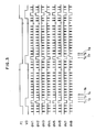
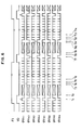
- the symbol FI indicates a field index signal. When this signal is high, it indicates an odd-numbered field, and when low, it indicates an even-numbered field.
- the symbol VD is a vertical synchronization signal.
- the voltage applied to the electrode ⁇ V1 to ⁇ V8 for the vertical transfer electrode correspond to the vertical transfer electrodes 1-8 to 1-15 shown in Figure 1.
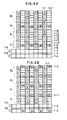
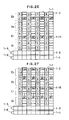
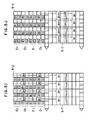
- the voltage applied to the electrode ⁇ V4 becomes high, for example, the charges r01, b01 stored in correspondence to the color filter array of red and blue of the horizontal second row of the odd-numbered field 01 are tansferred to the electrode of the transfer electrode 1-11.
- the signal charges of the vertical transfer CCD 1-2 are shifted four steps at time T3 of Figure 3. For this reason, the signal charges g01 obtained from the odd-numbered field 01 are transferred to the horizontal transfer CCD 1-4, and the charges r01, b01 are transferred to the horizontal transfer CCD 1-3 at the same time.
- the signal charges transferred to the horizontal transfer CCDs 1-3, 1-4 are horizontally transferred and read out to the outside for the time of the effective horizontal scanning duration of an image signal.
- the charge g02 obtained from the odd-numbered field 02 is transferred from the vertical transfer CCD 1-2 to the horizontal transfer CCD 1-4.
- the signal charges r02, b02 obtained from the odd-numbered field 02 are transferred from the vertical transfer CCD 1-2 to the horizontal transfer CCD 1-3, after which they are transferred to the outside by the horizontal transfer for the effective horizontal scanning duration of an image signal.
- Repetition of the above operation enables the signal charges corresponding to a green, red or blue signal read from the light receiving part of the odd-numbered fields 01, 02, --- to the vertical transfer CCDs to be read in turn into the outside in parallel by the horizontal transfer CCDs.
- the voltage applied to the electrode ⁇ V8 becomes high at time T7 as shown in Figure 2F.
- the charges rEl, bE1 stored for 1/30 sec. at the light receiving part 1-1 by the color filters made of red and blue colors are transferred below the electrode of the transfer electrode 1-15.
- the charge gE1 obtained from the horizontal first row of the even-numbered field E1 most near the horizontal transfer CCDs becomes in the state when they are transferred to the horizontal transfer CCD 1-4 exclusively used for a green signal.
- the pulses at time T8, T9 of Figure 3 are included in the same horizontal blanking duration.
- the charges of a green signal, a read signal, and a blue signal are transferred to the horizontal transfer CCDs 1-3, 1-4 of a two-step structure for each horizontal blanking duration in the order of the even-numbered fields E1, E2, ---.
- green signals, and red and blue signals are read in parallel by the horizontal transfer CCDs 1-3, 1-4 during a horizontal scanning.
- Figure 2I shows the states in which green signals, and red and blue signals are read over the horizontal scanning duration after the signal charges gE1, rE1, and bE1 read from the light receiving part of the even-numbered field E1 are transferred to the horizontal transfer CCDs 1-3, 1-4 as shown in Figure 2H.
- Figure 4 is a diagram illustrating the second embodiment of the present invention.
- the number of picture cells of the light receiving part in the vertical picture cell direction is about 960 (double) picture cells, and two steps of horizontal transfer CCDs are provided in the same way as for the solid-state image sensing device of Figure 1.
- different points are that the number of the vertical transfer steps of the light receiving part is 245 (half steps) and a store part is provided between the horizontal transfer CCDs of the two steps.
- the light receiving part 5-1 has about 960 light receiving elements in the vertical direction which are two times the number of the horizontal scanning lines. That is, the light receiving part 5-1 has about 960 picture cells in the vertical direction.
- This light receiving part 5-1 is formed of the odd-numbered field 01, the even-numbered field E1, the odd-numbered field 02, the even-numbered field E2, --- in sequence with the light receiving picture cells of horizontal two rows as a pair, and is provided with a color array in which the horizontal first row of each field is green (G), and the horizontal second row is made a repetition of red (R) and blue (B).
- the reference numeral 5-2 is a vertical transfer CCD. In this embodiment, it has 245 steps (half) for Figure 1, that is, the same number of conventional steps of Figure 7.
- the voltages to be applied to the electrode ⁇ VA1 to ⁇ VA4 are respectively applied to the vertical transfer electrodes 5-8 to 5-11 for four-phase driving.
- the first horizontal transfer CCD 5-3 is provided for red and blue signals in this embodiment.
- the reference numeral 5-6 shows a floating diffusion amplifier which serves as an output amplifier of the first horizontal transfer CCD 5-3.
- the reference numeral 5-7 is a store part. It is, for example, is formed of four-phase transfer electrodes 5-12 to 5-15 in correspondence with the odd-numbered field 01 and the even-numbered field E1, and the voltages to be applied to the electrode ⁇ VB1 to ⁇ VB4 are respectively applied to the transfer electrodes 5-12 to 5-15.
- Denoted by the reference numeral 5-4 is a horizontal transfer CCD, and is used for a green signal in this embodiment.
- Denoted by the reference numeral 5-5 is a floating diffusion amplifier which serves as an output amplifier of the second horizontal transfer CCD 5-4.
- the symbol FI indicates a field index signal, and when said signal is high, it indicates an odd-numbered field; when low, it indicates an even-numbered field.
- the symbol VD indicates a vertical synchronizaton signal; the symbols ⁇ VA1 to ⁇ VA4 indicate the voltages to be applied to the electrodes corresponding to the vertical transfer electrodes 5-8 to 5-11 of Figure 4.
- the symbols ⁇ VB1 to ⁇ VB4 indicate the voltage to be applied to the electrode to the transfer electrode of the store part 5-7, and correspond to the transfer electrodes 5-12 to 5-15 of Figure 4.
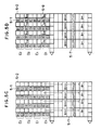
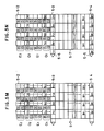
- the vertical transfer CCD 5-2 and the store part 5-7 are driven in high speed at times T2 to T3 of Figure 6, and as shown in Figure 5B, the charges g01, g02, g03, --- corresponding to the green signal on the vertical transfer CCD 5-2 are transferred to the store part 5-7.
- the solid-state image sensing device enters the state such that the signal charges g01 to g0245 corresponding to the green signal of the odd-numbered fields 01 to 0245 are all transferred to the store part 5-7.
- the voltage applied to the electrode ⁇ VA2 becomes high.
- the charges r01, b01 stored for 1/30 sec. on the corresponding light receiving part 5-1 are transferred below the transfer electrode 5-9 corresponding to the repetition of the color filters R, B of the horizontal second row in the odd-numbered field 01. This point applied to all the odd-numbered fields of the odd-numbered field 02 and those that follow.
- the signal charges r01, b01 of the vertical transfer part 5-2 of the odd-numbered field 01 most near the horizontal transfer CCDs are transferred to the first horizontal transfer CCD 5-3, and the signal charge g02 corresponding to the odd-numbered field 01 in the store part 5-7 is transferred to the second horizontal transfer CCD 5-4.
- This transfer to the horizontal transfer CCDs 5-3, 5-4 shown in Figure 5F is performed during the horizontal blanking.
- a green signal corresponding to the charge g01, and red and blue signals corresponding to the charges r01, b01 are read from the horizontal transfer CCDs 5-3, 5-4 in parallel to the outside during the effective horizontal scanning for the next image signal.
- the voltage applied to the electrode ⁇ VA3 becomes high at time T7 of Figure 6, and as shown in the even-numbered field E1 of Figure 5G, the charge gE1, corresponding to the green signal, stored for 1/30 sec. at the light receiving part 5-1 is transferred below the electrode of the transfer electrode 5-10.
- each of the charge gE1, gE2, --- read out from the light receiving part corresponding to the green signal of the even-numbered fields in Figure 5G is shifted one step in the vertical transfer CCD 5-2 at the timing of time T8 of Figure 6.
- the vertical transfer CCD 5-2 and the store part 5-7 are driven in high speed from the time T9 to T10 of Figure 6.
- the charges gE1 to gE245 corresponding to the green signal on the vertical transfer CCD 5-2 are transferred in turn to the store part 5-7 as shown in Figures 5I and 5J.
- the voltage applied to the electrode ⁇ VA4 becomes high at the time T11 of Figure 6, and the charges rE1, bE1 stored for 1/30 sec. at the light receiving part 5-1 made of a repetition of color filters R, B of the horizontal second row are transferred below the electrode of the transfer electrode 5-11 as shown in the even-numbered field E1 of Figure 5K.
- the charge gE1 of the store part 5-7 is transferred to the second horizontal transfer CCD 5-4 at time T13 of Figure 6 at the same time when the charges rE1, rb1 of the vertical transfer CCD 5-2 are transferred to the first horizontal transfer CCD 5-3.
- This transfer at time T13 is performed during the horizontal blanking, and the charge transferred onto the horizontal transfer CCDs 5-3, 5-4 during the next effective horizontal scanning are read out to the outside as shown in Figure 5N.
- the color filter array for the light receiving parts 1-1, 5-1 of the first embodiment of Figure 1 and the second embodiment of Figure 4 is made in such a way that for each of the odd-numbered field and the even-numbered field with the light receiving part of the horizontal two rows as a pair, the horizontal first row is all made green, and the horizontal second row is made a repetition of red and blue.
- the third embodiment is provided a color filter array such that the horizontal first row of the odd-numbered fields and the even-numbered fields is all made white (W), and the horizontal second row is made a repetition of red, blue, and green.
- the light receiving part of the color filter white (W) is made double-density. So, a resolution that can be used for the number of picture cells in the horizontal direction can be obtained, and particularly a brightness signal, i.e., a white signal itself can be obtained, further improving the color resolution.
- a green signal or a white signal corresponding to the same number of picture cells of the number of horizontal picture cells of a solid-state image sensing device can be obtained from the signal read into each of the odd-numbered fields and the even-numbered fields of a single solid-state image sensing device. Therefore, a color signal with a very high resolution can be obtained.
- the solid-state image sensing device since the green signal is output separately, the solid-state image sensing device has the advantage that signal processing can easily be performed.
Landscapes
- Engineering & Computer Science (AREA)
- Multimedia (AREA)
- Signal Processing (AREA)
- Physics & Mathematics (AREA)
- Spectroscopy & Molecular Physics (AREA)
- Color Television Image Signal Generators (AREA)
- Solid State Image Pick-Up Elements (AREA)
- Transforming Light Signals Into Electric Signals (AREA)
Applications Claiming Priority (2)
| Application Number | Priority Date | Filing Date | Title |
|---|---|---|---|
| JP243619/88 | 1988-09-28 | ||
| JP63243619A JPH0292087A (ja) | 1988-09-28 | 1988-09-28 | 固体撮像素子 |
Publications (2)
| Publication Number | Publication Date |
|---|---|
| EP0361938A2 true EP0361938A2 (de) | 1990-04-04 |
| EP0361938A3 EP0361938A3 (de) | 1990-12-19 |
Family
ID=17106515
Family Applications (1)
| Application Number | Title | Priority Date | Filing Date |
|---|---|---|---|
| EP19890309926 Withdrawn EP0361938A3 (de) | 1988-09-28 | 1989-09-28 | Festkörperbildaufnahmevorrichtung |
Country Status (2)
| Country | Link |
|---|---|
| EP (1) | EP0361938A3 (de) |
| JP (1) | JPH0292087A (de) |
Cited By (2)
| Publication number | Priority date | Publication date | Assignee | Title |
|---|---|---|---|---|
| GB2255872A (en) * | 1991-02-12 | 1992-11-18 | Mitsubishi Electric Corp | Solid-state imaging device |
| EP0599200A3 (de) * | 1992-11-20 | 1995-08-09 | Matsushita Electric Industrial Co Ltd | Festkörperbildaufnahmevorrichtung und Verfahren zu ihrem Betrieb. |
Family Cites Families (1)
| Publication number | Priority date | Publication date | Assignee | Title |
|---|---|---|---|---|
| US4064532A (en) * | 1974-09-18 | 1977-12-20 | Sony Corporation | Solid state color camera |
-
1988
- 1988-09-28 JP JP63243619A patent/JPH0292087A/ja active Pending
-
1989
- 1989-09-28 EP EP19890309926 patent/EP0361938A3/de not_active Withdrawn
Cited By (3)
| Publication number | Priority date | Publication date | Assignee | Title |
|---|---|---|---|---|
| GB2255872A (en) * | 1991-02-12 | 1992-11-18 | Mitsubishi Electric Corp | Solid-state imaging device |
| GB2255872B (en) * | 1991-02-12 | 1994-09-07 | Mitsubishi Electric Corp | Solid-state imaging device |
| EP0599200A3 (de) * | 1992-11-20 | 1995-08-09 | Matsushita Electric Industrial Co Ltd | Festkörperbildaufnahmevorrichtung und Verfahren zu ihrem Betrieb. |
Also Published As
| Publication number | Publication date |
|---|---|
| JPH0292087A (ja) | 1990-03-30 |
| EP0361938A3 (de) | 1990-12-19 |
Similar Documents
| Publication | Publication Date | Title |
|---|---|---|
| EP0812114B1 (de) | Festkörper-bildaufnahmevorrichtung,verfahren zur ansteuerung und festkörperkamera und kamerasystem | |
| EP0286123B1 (de) | Festkörper-Bildabtaster mit Hochgeschwindigkeitsverschluss und Verfahren zur Erzielung einer hohen Verschlussgeschwindigkeit in einem Festkörper-Bildabtaster | |
| US7079184B2 (en) | Image pickup device with vertical and horizontal charge transfer devices operable in plural modes | |
| US4837630A (en) | Solid-state imaging apparatus with a plurality of CCD storage sections | |
| US4032976A (en) | Smear reduction in ccd imagers | |
| US4985758A (en) | Signal processing system having selected output from plural readout devices | |
| EP0630151A2 (de) | Festkörperbildaufnehmer und Ansteuermethode für selbigen | |
| GB2186151A (en) | Solid state image pick-up arrangement | |
| US4641183A (en) | Image pick-up apparatus | |
| US7218348B2 (en) | Solid-state electronic imaging device and method of controlling opertion thereof | |
| US4531156A (en) | Solid state image pickup device | |
| US4117510A (en) | Solid state color imaging apparatus | |
| NL8201745A (nl) | Beeldopneeminrichting van het "solid state"-type. | |
| US7420607B2 (en) | Solid-state imaging element and digital camera | |
| US4910588A (en) | Image pick-up apparatus with high resolution and anti-bloom characteristics | |
| US5198890A (en) | White balance correcting device for an image sensing | |
| US5801850A (en) | Linear sensor having a plurality of sensor rows | |
| US6118481A (en) | Solid state image pick-up device and image pick-up apparatus | |
| US5796432A (en) | Method of and apparatus for solid state imaging device | |
| US8045025B2 (en) | Image pickup device adaptable to display fewer vertical pixels | |
| US4675887A (en) | Solid state imaging device and method with row-by-row charge transfer | |
| EP0441345A1 (de) | Standbild-Kamera mit hoher Auflösung | |
| US4853786A (en) | CSD image sensor and method of decreasing smear by the user thereof | |
| US6785027B1 (en) | Method for driving a CCD solid-state imaging device | |
| JPS5838026B2 (ja) | 色彩信号発生装置 |
Legal Events
| Date | Code | Title | Description |
|---|---|---|---|
| PUAI | Public reference made under article 153(3) epc to a published international application that has entered the european phase |
Free format text: ORIGINAL CODE: 0009012 |
|
| AK | Designated contracting states |
Kind code of ref document: A2 Designated state(s): DE FR GB |
|
| PUAL | Search report despatched |
Free format text: ORIGINAL CODE: 0009013 |
|
| AK | Designated contracting states |
Kind code of ref document: A3 Designated state(s): DE FR GB |
|
| 17P | Request for examination filed |
Effective date: 19910612 |
|
| 17Q | First examination report despatched |
Effective date: 19930721 |
|
| STAA | Information on the status of an ep patent application or granted ep patent |
Free format text: STATUS: THE APPLICATION IS DEEMED TO BE WITHDRAWN |
|
| 18D | Application deemed to be withdrawn |
Effective date: 19940201 |