EP0361947A2 - Synchrones Bemusterungssystem - Google Patents
Synchrones Bemusterungssystem Download PDFInfo
- Publication number
- EP0361947A2 EP0361947A2 EP89309952A EP89309952A EP0361947A2 EP 0361947 A2 EP0361947 A2 EP 0361947A2 EP 89309952 A EP89309952 A EP 89309952A EP 89309952 A EP89309952 A EP 89309952A EP 0361947 A2 EP0361947 A2 EP 0361947A2
- Authority
- EP
- European Patent Office
- Prior art keywords
- sampling
- pulses
- synchronizing
- received
- signal
- Prior art date
- Legal status (The legal status is an assumption and is not a legal conclusion. Google has not performed a legal analysis and makes no representation as to the accuracy of the status listed.)
- Granted
Links
Images


Classifications
-
- H—ELECTRICITY
- H04—ELECTRIC COMMUNICATION TECHNIQUE
- H04N—PICTORIAL COMMUNICATION, e.g. TELEVISION
- H04N7/00—Television systems
- H04N7/24—Systems for the transmission of television signals using pulse code modulation
Definitions
- This invention relates to digital sampling of analog communications signals, and more particularly to receiver-based sampling error elimination in video transmission systems having a specified number of intensity level time intervals per horizontal sweep.
- sampling and quantizing comprises converting continuous signals of time and amplitude into discrete quantized "stairsteps" uniformly sequenced in time.
- sampling alone does not necessarily entail loss of significant information as long as the sampling frequency is at least twice as great as the highest frequency of interest in the information signal.
- quantization does not cause a serious loss of information if the number of quantizing levels is sufficiently high.
- the quantized signal thus obtained may be, if desired, stored in the form of individual digital bytes in a digital memory. Information thus stored may be conveniently retrieved from the digital memory whenever needed.
- an analog transmission channel e.g. a coaxial cable or a radio link.
- the digital data will need to be reconverted to an analog video signal in order to display it on an analog display device.
- the digital memory is interrogated sequentially and the data is processed through a digital-to-analog (D/A) converter to recreate an analog stairstep video signal.
- D/A digital-to-analog
- the invention is directed to a synchronous sampling system located at the receiving end of an analog sampled data information channel.
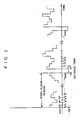
- a voltage-controllable sampling system pixel clock oscillator is forced by an automatic control system to have a predetermined number of pixel clock periods, with an accurancy that is within a small fraction of a clock period, between each horizontal sweep sync pulse contained in a received composite analog sampled-data stairstep video signal.
- the sampling system pixel clock oscillator is started at the trailing edge of each horizontal sync pulse and stopped at the leading edge of each ensuing horizontal sync pulse.
- the number of sampling system pixel clock periods between sequential horizontal sync pulses is counted and compared to a preset count.
- a difference therebetween is converted to a DC control voltage that automatically adjusts the sampling system pixel clock oscillator to conform closely to the sending system's predetermined number of pixel clock periods per horizontal data sweep.
- the analog to digital converter and the digital memory of the sampling system are thus synchronized to sample and store the received analog stairstep signal data well within the flat region of each stairstep.
- the horizontal sync pulses are detected by a standard sync stripper which triggers the sampling system's pixel clock oscillator as well as the system controller.
- the system controller resets the preset counter for each desired measurement and converts the preset counter's borrow output to a DC control voltage suitable for adjusting the sampling system's pixel clock oscillator to cause the oscillator to produce very nearly the preset number of pixel clock periods between horizontal sync pulses.
- the control system employed in the invention comprises a modified "bang-bang" system including an analog error signal integrator that is capable of homing the receiver sampler into a desired range with excellent accuracy.
- the invention is the simplest, most efficient, least expensive technique known to Applicant for accomplishing apparently flawless sampling of a received composite analog sampled-data stairstep video signal.
- ⁇ t's t n - t n-1 ) that are applied progressing uniformly in time and space, from left to right across the display device (e.g. a cathode ray tube [CRT] screen).
- the display device e.g. a cathode ray tube [CRT] screen.
- Receiving and displaying video data as described above is well known to video system engineers.
- the difficulty occurs not so much in displaying the received video image as it does in capturing and storing the image data in digital form so that an entirely faithful and stable reproduction of the originally received stairstep analog video image data content may be obtained upon demand by simply interrogating a digital memory (i.e. a digital data storage device).
- a digital memory i.e. a digital data storage device
- the instant invention makes use of the fact that the number of pixel clock periods per transmitted horizontal video data line is known to be precisely 900 sequential periods equally spaced in time.
- the pixel clock of the receiving and storing system is coerced to also have almost exactly 900 periods between the end of a received horizontal sync pulse and the start of the immediately subsequent received horizontal sync pulse.
- This oscillator is a simple pulse generator that is DC voltage controllable over a range of 2 MHz to 40 MHz corresponding to a DC input range of OV to 3V.
- the design of such oscillators is well known to those of ordinary skill in the electronics arts.
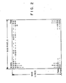
- Sync stripper 305 includes a standard device for detecting the sync signals from a composite video signal.
- the one used by Applicant is the National Semiconductor Co. Model No. LM 1881.
- sync stripper 305 on horizontal sync output line 308 is used to enable the receiving and storing pixel clock oscillator 301 only during each received video line.
- One preferred embodiment of the invention cludes a simple adjustable pulse delay network 315, as is well known to those skilled in the electronics arts, which provides the ability to shift the sample timing points in the direction of the center of the stairstep periods of the received video signal.
- the pixel frequency of the source video signal is approximately known (i.e., within about 10%). This is normally the case, so initial adjustment of the receiver sampling rate and phase can be accomplished rapidly.
- a perfectly sampled text image will produce only two signal levels, while an aliased text image will produce intermediate signals. If the sampling frequency is more than the equivalent of 2 pixels/line in error, the sample signal will display a nodal pattern on the receiver monitor screen with the number of nodes equalling the frequency error. However, the number of sampled signal maxima or minima is relatively independent of the error except at an error of 2 or 1 pixels/line, where the number of either maxima or minima will change significantly. Monitoring the overflow signal of the A/D converter with a Dc voltmeter will provide an indication of the number of times the input signal exceeds the range of the A/D converter.
- the voltmeter When the input signal is aliased, there are fewer than the maximum overflow events, so the voltmeter reads relatively lower. As the sampling frequency approaches the source generator rate, signficantly more plentiful overflow events will occur, thus raising the measured voltage. When the frequency is within one pixel/line, the sampling frequency is correct, but the phase of the sampling clock may be in error. Adjusting the PHASE control to maximize the DC voltmeter reading will assure that all text pixels are being sampled at their correct signal value.
- the output on vertical sync outputline 309 of sync stripper 305 is used to trigger controller 304 which in turn resets itself after each video field, reloads the preset counter 302 and applies a compensating DC control voltage along line 310 to the receiving and storing pixel clock oscillator 301.
- D flip-flop 401 is triggered via line 303 by the borrow output of preset counter 302.
- the output of D flip-flop 401 is transferred from its inverting output terminal along line 402 to electronic switch 403.
- switch 403 When switch 403 is closed, its output along line 405 to resistor 404 and capacitor 406 is either 0 volts or +5 volts, depending on the state of D-flip-flop 401 output on line 402.
- Switch 403 is enabled only briefly after each video field via one-shot 408 which is triggered via sync stripper output line 309.
- the second one-shot 409 is used to reset D flip-flop 401 via line 410 as well as to reset preset counter 302 via line 311 after each video field.
- the gain of this "bang-bang" feedback system can be adjusted simply by adjusting the length of operation of oneshot 408, thus accomplishing the desired precision for the number of pixel clock periods generated by receiving and storing pixel clock oscillator 301 per received video signal period. Typically, a correction of ⁇ 0.1 pixel period/field is effected.
- the receiving pixel clock oscillator can be caused to stay well within the range of 899.9 to 900.1 pixel clock periods per received video image field. This accuracy assures accurate sampling of each and every received stairstep voltage level well into its respective flat region. As a result, the received analog video signal data is accurately and reliably converted by A/D converter 306 into corresponding digital data that is stored in digital memory 307 for any desired future use.
- the instant invention has been installed by Applicant into a high resolution medical imaging system with excellent results.
- the resulting images obtained from the digital memory are entirely without blemishes that would otherwise be present due to aliasing or other inadequate sampling methods.
Landscapes
- Engineering & Computer Science (AREA)
- Multimedia (AREA)
- Signal Processing (AREA)
- Analogue/Digital Conversion (AREA)
- Compression Or Coding Systems Of Tv Signals (AREA)
- Color Television Systems (AREA)
- Television Systems (AREA)
Applications Claiming Priority (2)
| Application Number | Priority Date | Filing Date | Title |
|---|---|---|---|
| US251961 | 1988-09-29 | ||
| US07/251,961 US4905085A (en) | 1988-09-29 | 1988-09-29 | Synchronous sampling system |
Publications (3)
| Publication Number | Publication Date |
|---|---|
| EP0361947A2 true EP0361947A2 (de) | 1990-04-04 |
| EP0361947A3 EP0361947A3 (de) | 1991-05-02 |
| EP0361947B1 EP0361947B1 (de) | 1994-11-30 |
Family
ID=22954097
Family Applications (1)
| Application Number | Title | Priority Date | Filing Date |
|---|---|---|---|
| EP89309952A Expired - Lifetime EP0361947B1 (de) | 1988-09-29 | 1989-09-29 | Synchrones Bemusterungssystem |
Country Status (4)
| Country | Link |
|---|---|
| US (1) | US4905085A (de) |
| EP (1) | EP0361947B1 (de) |
| JP (1) | JP2574038B2 (de) |
| DE (1) | DE68919626T2 (de) |
Cited By (1)
| Publication number | Priority date | Publication date | Assignee | Title |
|---|---|---|---|---|
| WO1995001047A3 (en) * | 1993-06-10 | 1995-03-02 | Barco | A method and a device for converting a picture |
Families Citing this family (16)
| Publication number | Priority date | Publication date | Assignee | Title |
|---|---|---|---|---|
| JPH05308599A (ja) * | 1991-12-30 | 1993-11-19 | Samsung Electron Co Ltd | プリンティング方法及びこれに適合したプリンティング装置 |
| US5551016A (en) * | 1993-07-01 | 1996-08-27 | Queen's University At Kingston | Monitoring system and interface apparatus therefor |
| JP3149124B2 (ja) * | 1995-03-06 | 2001-03-26 | 株式会社コンテック | 色信号サンプリング方法 |
| US5786868A (en) * | 1995-12-22 | 1998-07-28 | Cirrus Logic, Inc. | Automatic step generator for self-correction of sampling |
| JPH09231691A (ja) * | 1996-02-27 | 1997-09-05 | Hewlett Packard Japan Ltd | 記憶装置測定装置 |
| JP3358432B2 (ja) * | 1996-02-29 | 2002-12-16 | ソニー株式会社 | クロック信号発生装置及び方法 |
| US5767916A (en) * | 1996-03-13 | 1998-06-16 | In Focus Systems, Inc. | Method and apparatus for automatic pixel clock phase and frequency correction in analog to digital video signal conversion |
| US5805233A (en) * | 1996-03-13 | 1998-09-08 | In Focus Systems, Inc. | Method and apparatus for automatic pixel clock phase and frequency correction in analog to digital video signal conversion |
| US6965400B1 (en) * | 1997-02-07 | 2005-11-15 | Canon Kabushiki Kaisha | Video input apparatus and image pickup system including the apparatus |
| US6633288B2 (en) * | 1999-09-15 | 2003-10-14 | Sage, Inc. | Pixel clock PLL frequency and phase optimization in sampling of video signals for high quality image display |
| US6636205B1 (en) | 2000-04-10 | 2003-10-21 | Infocus Corporation | Method and apparatus for determining a clock tracking frequency in a single vertical sync period |
| TW558712B (en) * | 2001-01-05 | 2003-10-21 | Benq Corp | Method for automatically adjusting display quality |
| JP2011154060A (ja) * | 2010-01-26 | 2011-08-11 | Canon Inc | 表示装置 |
| CN112446235A (zh) * | 2019-08-28 | 2021-03-05 | 广东博智林机器人有限公司 | 基于psd的信号峰峰值获取装置、方法和光斑重心检测方法 |
| CN114035474B (zh) * | 2021-11-10 | 2024-06-14 | 中国科学院微电子研究所 | 采样信号同步控制系统 |
| CN115037840B (zh) * | 2022-04-29 | 2023-02-28 | 北京航空航天大学 | 扫描成像联用系统的数据同步方法、装置及扫描成像联用系统 |
Family Cites Families (17)
| Publication number | Priority date | Publication date | Assignee | Title |
|---|---|---|---|---|
| US3259851A (en) * | 1961-11-01 | 1966-07-05 | Avco Corp | Digital system for stabilizing the operation of a variable frequency oscillator |
| US3287655A (en) * | 1964-11-30 | 1966-11-22 | Douglas A Venn | Digital control for disciplining oscillators |
| US3978519A (en) * | 1974-03-16 | 1976-08-31 | Quantel Limited | Digital time base correctors for television equipment |
| GB1465314A (en) * | 1974-03-16 | 1977-02-23 | Quantel Ltd | Digital time base correctors for television equipment |
| US4074307A (en) * | 1975-08-14 | 1978-02-14 | Rca Corporation | Signal processor using charge-coupled devices |
| GB1515584A (en) * | 1976-01-28 | 1978-06-28 | Quantel Ltd | Time base corrector |
| US4105946A (en) * | 1977-07-06 | 1978-08-08 | Sansui Electric Co., Ltd. | Frequency synthesizer with phase locked loop and counter |
| US4253116A (en) * | 1979-11-27 | 1981-02-24 | Rca Corporation | Television synchronizing system operable from nonstandard signals |
| DE3171427D1 (en) * | 1981-11-19 | 1985-08-22 | Itt Ind Gmbh Deutsche | Digital circuit delivering a binary signal whenever the frequency ration of the line/and the field frequency occurs |
| JPS58191573A (ja) * | 1982-05-06 | 1983-11-08 | Victor Co Of Japan Ltd | 水平走査周波数逓倍回路 |
| JPS60160220A (ja) * | 1984-01-31 | 1985-08-21 | Fujitsu Ltd | ドリフト検出回路 |
| US4528521A (en) * | 1984-02-09 | 1985-07-09 | At&T Information Systems Inc. | Precision control frequency synthesizer having an unstable, variable frequency input signal |
| GB8414449D0 (en) * | 1984-06-06 | 1984-07-11 | Motorola Inc | Voltage controlled oscillator |
| JPS6133575U (ja) * | 1984-07-28 | 1986-02-28 | ソニー株式会社 | クロツク形成回路 |
| JPS6153817A (ja) * | 1984-08-23 | 1986-03-17 | Nec Corp | タイミング発生装置 |
| JPS62172875A (ja) * | 1986-01-27 | 1987-07-29 | Nippon Hoso Kyokai <Nhk> | 多重サブサンプル伝送信号の再生方法 |
| JPS6277635A (ja) * | 1985-10-01 | 1987-04-09 | Seiko Instr & Electronics Ltd | ビデオ信号サンプリングクロツク位相補正回路 |
-
1988
- 1988-09-29 US US07/251,961 patent/US4905085A/en not_active Expired - Lifetime
-
1989
- 1989-09-29 JP JP1252476A patent/JP2574038B2/ja not_active Expired - Fee Related
- 1989-09-29 EP EP89309952A patent/EP0361947B1/de not_active Expired - Lifetime
- 1989-09-29 DE DE68919626T patent/DE68919626T2/de not_active Expired - Fee Related
Cited By (2)
| Publication number | Priority date | Publication date | Assignee | Title |
|---|---|---|---|---|
| WO1995001047A3 (en) * | 1993-06-10 | 1995-03-02 | Barco | A method and a device for converting a picture |
| US5801780A (en) * | 1993-06-10 | 1998-09-01 | Barco | Method and a device for converting a picture |
Also Published As
| Publication number | Publication date |
|---|---|
| JP2574038B2 (ja) | 1997-01-22 |
| US4905085A (en) | 1990-02-27 |
| JPH02170689A (ja) | 1990-07-02 |
| EP0361947A3 (de) | 1991-05-02 |
| EP0361947B1 (de) | 1994-11-30 |
| DE68919626D1 (de) | 1995-01-12 |
| DE68919626T2 (de) | 1995-06-01 |
Similar Documents
| Publication | Publication Date | Title |
|---|---|---|
| US4905085A (en) | Synchronous sampling system | |
| JP3220023B2 (ja) | 液晶表示装置 | |
| US3984624A (en) | Video system for conveying digital and analog information | |
| US5579348A (en) | Method and apparatus for improving the apparent accuracy of a data receiver clock circuit | |
| EP0473338A2 (de) | Bitsynchronisierung mittels elastisches Speichers | |
| JPH06188870A (ja) | クロック再生器 | |
| US5767917A (en) | Method and apparatus for multi-standard digital television synchronization | |
| EP0138164B1 (de) | Verfahren und Gerät für die Abtastung und Verarbeitung eines Videosignals | |
| EP0360519B1 (de) | Zeitmessung zur Anzeige des Jitters | |
| EP0378875B1 (de) | Rauschmessung für Videosignale | |
| US4713691A (en) | Interface circuit of video signal hard copy apparatus | |
| US3863022A (en) | Television signal clocked delay line for delay by an integer number of horizontal scanning lines driven by a pilot signal | |
| US5068717A (en) | Method and apparatus for synchronization in a digital composite video system | |
| US4874992A (en) | Closed loop adaptive raster deflection signal generator | |
| KR100466553B1 (ko) | 지연 정정 회로 | |
| GB2050729A (en) | Television horizontal afpc systems | |
| EP1205065B1 (de) | Vorrichtung und verfahren zur erzeugung eines taktsignals mit hoher frequenzgenauigkeit | |
| US4198659A (en) | Vertical synchronizing signal detector for television video signal reception | |
| EP0217091A1 (de) | Korrekturkreis für Geschwindigkeitsfehler in einem Zeitbasiskorrektor | |
| US3991270A (en) | Circuit arrangement for line synchronization in a television receiver | |
| FR2571162A1 (fr) | Circuit de base de temps permettant de faire varier le format horizontal d'un visuel a balayage par trame. | |
| CN85101811A (zh) | 采样处理视频信号的方法及设备 | |
| JPH07307727A (ja) | データ信号のサンプリング方法及びその回路 | |
| JPS6335135B2 (de) | ||
| JPS60163577A (ja) | 水平同期信号挿入方法 |
Legal Events
| Date | Code | Title | Description |
|---|---|---|---|
| PUAI | Public reference made under article 153(3) epc to a published international application that has entered the european phase |
Free format text: ORIGINAL CODE: 0009012 |
|
| AK | Designated contracting states |
Kind code of ref document: A2 Designated state(s): BE DE ES FR GB IT NL SE |
|
| PUAL | Search report despatched |
Free format text: ORIGINAL CODE: 0009013 |
|
| AK | Designated contracting states |
Kind code of ref document: A3 Designated state(s): BE DE ES FR GB IT NL SE |
|
| 17P | Request for examination filed |
Effective date: 19910515 |
|
| 17Q | First examination report despatched |
Effective date: 19930518 |
|
| GRAA | (expected) grant |
Free format text: ORIGINAL CODE: 0009210 |
|
| AK | Designated contracting states |
Kind code of ref document: B1 Designated state(s): BE DE ES FR GB IT NL SE |
|
| PG25 | Lapsed in a contracting state [announced via postgrant information from national office to epo] |
Ref country code: IT Free format text: LAPSE BECAUSE OF FAILURE TO SUBMIT A TRANSLATION OF THE DESCRIPTION OR TO PAY THE FEE WITHIN THE PRESCRIBED TIME-LIMIT;WARNING: LAPSES OF ITALIAN PATENTS WITH EFFECTIVE DATE BEFORE 2007 MAY HAVE OCCURRED AT ANY TIME BEFORE 2007. THE CORRECT EFFECTIVE DATE MAY BE DIFFERENT FROM THE ONE RECORDED. Effective date: 19941130 Ref country code: ES Free format text: THE PATENT HAS BEEN ANNULLED BY A DECISION OF A NATIONAL AUTHORITY Effective date: 19941130 Ref country code: BE Effective date: 19941130 Ref country code: NL Effective date: 19941130 |
|
| REF | Corresponds to: |
Ref document number: 68919626 Country of ref document: DE Date of ref document: 19950112 |
|
| ET | Fr: translation filed | ||
| PG25 | Lapsed in a contracting state [announced via postgrant information from national office to epo] |
Ref country code: SE Effective date: 19950228 |
|
| NLV1 | Nl: lapsed or annulled due to failure to fulfill the requirements of art. 29p and 29m of the patents act | ||
| PLBE | No opposition filed within time limit |
Free format text: ORIGINAL CODE: 0009261 |
|
| STAA | Information on the status of an ep patent application or granted ep patent |
Free format text: STATUS: NO OPPOSITION FILED WITHIN TIME LIMIT |
|
| 26N | No opposition filed | ||
| REG | Reference to a national code |
Ref country code: GB Ref legal event code: 732E |
|
| REG | Reference to a national code |
Ref country code: FR Ref legal event code: TP |
|
| PGFP | Annual fee paid to national office [announced via postgrant information from national office to epo] |
Ref country code: FR Payment date: 19990909 Year of fee payment: 11 |
|
| PGFP | Annual fee paid to national office [announced via postgrant information from national office to epo] |
Ref country code: GB Payment date: 19990929 Year of fee payment: 11 |
|
| PGFP | Annual fee paid to national office [announced via postgrant information from national office to epo] |
Ref country code: DE Payment date: 19991001 Year of fee payment: 11 |
|
| PG25 | Lapsed in a contracting state [announced via postgrant information from national office to epo] |
Ref country code: GB Free format text: LAPSE BECAUSE OF NON-PAYMENT OF DUE FEES Effective date: 20000929 |
|
| REG | Reference to a national code |
Ref country code: GB Ref legal event code: 732E |
|
| GBPC | Gb: european patent ceased through non-payment of renewal fee |
Effective date: 20000929 |
|
| PG25 | Lapsed in a contracting state [announced via postgrant information from national office to epo] |
Ref country code: FR Free format text: LAPSE BECAUSE OF NON-PAYMENT OF DUE FEES Effective date: 20010531 |
|
| PG25 | Lapsed in a contracting state [announced via postgrant information from national office to epo] |
Ref country code: DE Free format text: LAPSE BECAUSE OF NON-PAYMENT OF DUE FEES Effective date: 20010601 |
|
| REG | Reference to a national code |
Ref country code: FR Ref legal event code: ST |
|
| REG | Reference to a national code |
Ref country code: FR Ref legal event code: TP |