EP0362512A1 - Appareil pour le revêtement électrolytique de pièces en forme de plaque, notamment de cartes de circuits imprimés - Google Patents
Appareil pour le revêtement électrolytique de pièces en forme de plaque, notamment de cartes de circuits imprimés Download PDFInfo
- Publication number
- EP0362512A1 EP0362512A1 EP89114377A EP89114377A EP0362512A1 EP 0362512 A1 EP0362512 A1 EP 0362512A1 EP 89114377 A EP89114377 A EP 89114377A EP 89114377 A EP89114377 A EP 89114377A EP 0362512 A1 EP0362512 A1 EP 0362512A1
- Authority
- EP
- European Patent Office
- Prior art keywords
- contact
- workpieces
- contacting
- contact means
- electrolyte solution
- Prior art date
- Legal status (The legal status is an assumption and is not a legal conclusion. Google has not performed a legal analysis and makes no representation as to the accuracy of the status listed.)
- Granted
Links
Images
Classifications
-
- C—CHEMISTRY; METALLURGY
- C25—ELECTROLYTIC OR ELECTROPHORETIC PROCESSES; APPARATUS THEREFOR
- C25D—PROCESSES FOR THE ELECTROLYTIC OR ELECTROPHORETIC PRODUCTION OF COATINGS; ELECTROFORMING; APPARATUS THEREFOR
- C25D17/00—Constructional parts, or assemblies thereof, of cells for electrolytic coating
- C25D17/16—Apparatus for electrolytic coating of small objects in bulk
- C25D17/28—Apparatus for electrolytic coating of small objects in bulk with means for moving the objects individually through the apparatus during treatment
-
- H—ELECTRICITY
- H05—ELECTRIC TECHNIQUES NOT OTHERWISE PROVIDED FOR
- H05K—PRINTED CIRCUITS; CASINGS OR CONSTRUCTIONAL DETAILS OF ELECTRIC APPARATUS; MANUFACTURE OF ASSEMBLAGES OF ELECTRICAL COMPONENTS
- H05K3/00—Apparatus or processes for manufacturing printed circuits
- H05K3/22—Secondary treatment of printed circuits
- H05K3/24—Reinforcing of the conductive pattern
- H05K3/241—Reinforcing of the conductive pattern characterised by the electroplating method; means therefor, e.g. baths or apparatus
Definitions
- the invention relates to an electroplating device for plate-shaped workpieces to be treated in a horizontal pass, in particular printed circuit boards a transport device for transporting the workpieces through an electrolyte solution, - At least one contacting device arranged on the side of the continuous path for cathodic contacting of the workpieces and with - A cover arranged on the side of the continuous path to protect the contact means of the contacting device from the entry of electrolyte solution.
- the contacting device for cathodic contacting of the workpieces is formed by pliers-shaped contact clamps which can be moved laterally with the respective workpiece, an endless drive preferably serving as a movable carrier of the contact clamps.
- means are provided at the beginning and end of the transport path of the plate-shaped workpieces which cause the side edge of the workpieces to be gripped by the contact terminals or the workpieces to be released by the contact terminals.
- the contact terminals can also serve as transport elements for the passage of the workpieces.
- the contact terminals are shielded from the ingress of electrolyte solution by a gasket that extends laterally in the direction of flow and rests resiliently on the respective workpiece.
- Another galvanizing device is known from DE-A-36 24 481, in which the transport device is designed as an endlessly rotating, driven row of individual transport members is formed, which hold the side edges of the plate-shaped workpieces and move in the transport direction, with means being provided at the beginning and end of the transport path of the plate-shaped workpieces located in the electrolysis chamber, which enable the plate-shaped workpieces to be gripped by the transport members or to release the plate-shaped parts Work pieces through the transport organs. Apart from the start of gripping or the beginning of releasing, there is no relative movement between the transport members and the workpiece edges, so that wear and tear or wear and tear of the transport members are avoided. The transport members can then also serve to supply current to the plate-shaped workpieces.
- the invention is based on the object of designing the contacting device of a generic electroplating device in such a way that reliable cathodic contacting of the workpieces is ensured with little effort.
- the contact brushes or contact springs running with the workpiece have the particular advantage that they do not require any actuating devices at the beginning and end of the transport path and that they can be cleaned when they return. By cleaning the contact means in this way, the cathodic contacting of the workpieces can be decisively improved.
- contact brushes or contact springs run synchronously with the workpiece, there is no relative movement between the contact means and the workpiece edges, ie wear Appearances or signs of abrasion of the contact means are avoided.
- contact brushes are provided in the form of an endlessly rotating brush strip, which slides in the contacting area on a busbar arranged on the rear.
- a very reliable cathodic contacting of the workpieces can also be achieved in that on an endlessly circulating metal band, mutually opposite contact springs are attached, which bear resiliently on the top and bottom of the workpieces.
- a further preferred embodiment of the invention is characterized by a cleaning device designed as an electrolytic demetallization cell. This results in a particularly reliable electrochemical copper removal of the contact means during the return.
- a further significant reduction in the structural complexity of the entire electroplating device is achieved by a transport device consisting of an upper belt drive and a lower belt drive for the frictional entrainment of the workpieces between the lower run of the upper belt drive and the upper run of the lower belt drive, in each case between the upper run and the lower run Run of the belt drives a sealing wall is arranged.
- a particularly effective shielding of the contacting device is thus carried out here by sealing tapes firmly pressed against the surface of the workpieces, these sealing tapes simultaneously effecting the frictional entrainment of the workpieces as transport members.
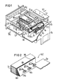
- Fig. 1 shows a perspective view of the electroplating device of a horizontal continuous system for through-plating and electroplating circuit boards Lp. It can be seen that the two end walls of a bath container Bb are provided with horizontal slots Sz at the level of a horizontal pass-through path indicated by arrows Pf1, which enable the printed circuit boards Lp to pass through.
- the interior between an upper cover hood (not shown in FIG. 1) and the bath container Bb receiving an electrolyte solution is provided on one side with a suction Ag, which is connected to a central suction device for generating a negative pressure in this space. Below the suction Ag, a longitudinally extending drive shaft Aw can be seen, which drives the two upper guide rollers Ur shown in FIG.
- Each of these two upper deflection rollers Ur shown belongs to a laterally arranged transport device Te, which transports the printed circuit boards Lp through the electrolyte solution in the direction of the arrows Pf1.
- Each of these transport devices Te arranged on both sides of the continuous path Pf1 consists of an upper belt drive Bto and a lower belt drive Btu, the two belt drives each having a belt B which runs endlessly over two deflection rollers Ur arranged at a distance from one another.
- the belt drives mentioned are each driven via the drive shaft Aw in such a way that the printed circuit boards Lp entering through the front slot Sz in the direction of passage Pf1 are drawn in between the belt drives Bto and Btu and between the horizontal lower run of the upper belt drive Bto and the horizontal upper run of the lower belt drive Btu in the direction of arrow P1 are frictionally carried.
- the strips B lie in the side region of the printed circuit board Lp over the entire length close to the top and the bottom, so that no electrolyte solution can pass between the strip B and the printed circuit board Lp.
- an upper plate Po extending transversely to the direction of passage Pf1, on the upper side of which the upper runs lie tightly.
- Sealing walls Dw each extend between the underside of the upper plate Po and the lower runs of the upper belt drives Bto.
- the lower runs of the lower belt drives Btu lie with their underside close to the bottom Bo of the bath container Bb and with their upper side close to one lower plate Pu extending transversely to the direction of passage Pf1.
- sealing walls Dw are arranged between the lower plate Pu and the upper runs of the lower belt drives Btu. It can thus be readily seen that the upper belt drives Bto and the lower belt drives Btu form a shield or cover in conjunction with the upper plate Po or the lower plate Pu and the sealing walls Dw, which at least largely prevents the lateral leakage of electrolyte solution .
- Fig. 1 also shows that between the sealing walls Dw at a short distance above the path Pf1 of the circuit boards Lp is a horizontally aligned upper anode Ao, which consists of a basket made of expanded metal and spherical anode material contained therein.
- the upper plate Po is provided with an opening which can be closed by a cover De.
- the lower anode Au is also a horizontally aligned lower anode Au, which is designed as an expanded metal screen and consists, for example, of platinized titanium.
- the lower anode Au is an insoluble anode.
- the cathodic contacting of the printed circuit boards Lp takes place via a contacting device Kv1 arranged on the right in the direction of passage Pf1, the contact means of which contact the side edges of the printed circuit boards Lp which project beyond the transport device Te.
- a second contacting device Kv1 which cannot be seen in FIG. 1, is expediently arranged on the left side of the through path Pf1.
- the contacting device Kv1 comprises contact brushes Kb in the form of a brush belt running endlessly over two rollers Ro.
- the rear roller Ro shown in FIG. 1 is driven in the direction of arrow Pf3 in such a way that the brush belt with the contact brushes Kb runs synchronously with the printed circuit boards Lp.
- the cathode current is supplied via a stationary busbar Ss to the brush strip sliding thereon and from its contact brushes Kb to the top and bottom of the respective printed circuit board Lp.
- This cleaning device RE is designed as an electrolytic demetallization cell which contains an electrolyte solution, preferably the electrolyte solution used for the electroplating. The demetallization then takes place by anodic contacting of the brush strip relative to a cathode located in the cleaning device RE.
- contact means which run synchronously with the printed circuit boards Lp.
- These contact means are formed by a plurality of pairs of contact springs fastened at a distance from one another on an endlessly circulating metal strip Mb.
- Each pair of contact springs consists of an upper contact spring Kfo and an opposite lower contact spring Kfu, which receive the side edges of the printed circuit boards Lp while maintaining a certain resilient contact pressure between them.
- the power supply to the metal strip Mb takes place via a busbar Ss and brushes Brs arranged in a fixed position on the rear. A supply via springs would of course also be possible.
- the busbar Ss is preferably formed by a titanium-coated solid copper conductor.
- the brushes Brs are preferably made of copper, while for the metal strip Mb and the contact springs Kfo and Kfu titanium has proven to be a very good material.
- a cleaning or metallization of the contact springs Kfo and Kfu is also possible here according to the principle shown in Fig. 1.
Landscapes
- Engineering & Computer Science (AREA)
- Chemical & Material Sciences (AREA)
- Materials Engineering (AREA)
- Microelectronics & Electronic Packaging (AREA)
- Chemical Kinetics & Catalysis (AREA)
- Electrochemistry (AREA)
- Manufacturing & Machinery (AREA)
- Metallurgy (AREA)
- Organic Chemistry (AREA)
- Electroplating Methods And Accessories (AREA)
- Manufacturing Of Printed Wiring (AREA)
- Coating With Molten Metal (AREA)
- Manufacturing Of Printed Circuit Boards (AREA)
Priority Applications (1)
| Application Number | Priority Date | Filing Date | Title |
|---|---|---|---|
| AT89114377T ATE89615T1 (de) | 1988-09-01 | 1989-08-03 | Galvanisiereinrichtung fuer plattenfoermige werkstuecke, insbesondere leiterplatten. |
Applications Claiming Priority (2)
| Application Number | Priority Date | Filing Date | Title |
|---|---|---|---|
| DE3829761 | 1988-09-01 | ||
| DE3829761 | 1988-09-01 |
Publications (2)
| Publication Number | Publication Date |
|---|---|
| EP0362512A1 true EP0362512A1 (fr) | 1990-04-11 |
| EP0362512B1 EP0362512B1 (fr) | 1993-05-19 |
Family
ID=6362103
Family Applications (1)
| Application Number | Title | Priority Date | Filing Date |
|---|---|---|---|
| EP19890114377 Expired - Lifetime EP0362512B1 (fr) | 1988-09-01 | 1989-08-03 | Appareil pour le revêtement électrolytique de pièces en forme de plaque, notamment de cartes de circuits imprimés |
Country Status (5)
| Country | Link |
|---|---|
| US (1) | US4948483A (fr) |
| EP (1) | EP0362512B1 (fr) |
| JP (1) | JPH02111895A (fr) |
| AT (1) | ATE89615T1 (fr) |
| DE (1) | DE58904414D1 (fr) |
Cited By (3)
| Publication number | Priority date | Publication date | Assignee | Title |
|---|---|---|---|---|
| EP0361029B1 (fr) * | 1988-09-01 | 1993-05-19 | Siemens Nixdorf Informationssysteme Aktiengesellschaft | Appareil pour le revêtement électrolytique de pièces en forme de plaque, notamment de cartes de circuits imprimés |
| EP0561184A1 (fr) * | 1992-03-14 | 1993-09-22 | Gebr. Schmid GmbH & Co. | Dispositif pour le traitement d'objets, en particulier dispositifs de métallisation pour plaques de circuit |
| DE19724059B4 (de) * | 1997-06-07 | 2006-07-20 | Hans Höllmüller Maschinenbau GmbH & Co | Vorrichtung zum Galvanisieren von elektronischen Leiterplatten |
Families Citing this family (6)
| Publication number | Priority date | Publication date | Assignee | Title |
|---|---|---|---|---|
| US5223116A (en) * | 1992-05-11 | 1993-06-29 | Siemens Aktiengesellschaft | Apparatus for electrophoretic application of a lacquer onto plate-shaped work pieces |
| EP0728852A1 (fr) * | 1995-02-27 | 1996-08-28 | Yamaha Hatsudoki Kabushiki Kaisha | Dispositif de revêtement et dispositif pour son alimentation en grenailles |
| DE05075545T1 (de) | 1998-05-20 | 2006-08-31 | Process Automation International Ltd., Tai Po | Vorrichtung zur Elektroplattierung |
| US6261425B1 (en) | 1998-08-28 | 2001-07-17 | Process Automation International, Ltd. | Electroplating machine |
| DE19840471A1 (de) * | 1998-09-04 | 2000-03-09 | Schmid Gmbh & Co Geb | Einrichtung zum Abtrag einer Beschichtung von Gegenständen |
| DE202007003178U1 (de) * | 2007-03-01 | 2008-10-23 | Polman, Eckhard | Bandförderer |
Citations (4)
| Publication number | Priority date | Publication date | Assignee | Title |
|---|---|---|---|---|
| GB1482958A (en) * | 1974-05-31 | 1977-08-17 | Auric Corp | Electroplating apparatus |
| GB2149820A (en) * | 1983-11-11 | 1985-06-19 | Cockerill Sambre Sa | Feeding current to metal strip in electroplating device |
| EP0254030A1 (fr) * | 1986-07-19 | 1988-01-27 | Schering Aktiengesellschaft | Dispositif de traitement électrolytique d'objets en forme de plaques |
| EP0254962B1 (fr) * | 1986-07-28 | 1991-12-18 | Siemens Aktiengesellschaft | Dispositif pour l'électroplacage des articles en forme de plaques, en particulier des plaques de circuits imprimés |
Family Cites Families (2)
| Publication number | Priority date | Publication date | Assignee | Title |
|---|---|---|---|---|
| US4385967A (en) * | 1981-10-07 | 1983-05-31 | Chemcut Corporation | Electroplating apparatus and method |
| DE58904413D1 (de) * | 1988-09-01 | 1993-06-24 | Siemens Nixdorf Inf Syst | Galvanisiereinrichtung fuer plattenfoermige werkstuecke, insbesondere leiterplatten. |
-
1989
- 1989-08-03 EP EP19890114377 patent/EP0362512B1/fr not_active Expired - Lifetime
- 1989-08-03 DE DE8989114377T patent/DE58904414D1/de not_active Expired - Fee Related
- 1989-08-03 AT AT89114377T patent/ATE89615T1/de not_active IP Right Cessation
- 1989-08-16 US US07/394,725 patent/US4948483A/en not_active Expired - Fee Related
- 1989-08-29 JP JP1222771A patent/JPH02111895A/ja active Pending
Patent Citations (4)
| Publication number | Priority date | Publication date | Assignee | Title |
|---|---|---|---|---|
| GB1482958A (en) * | 1974-05-31 | 1977-08-17 | Auric Corp | Electroplating apparatus |
| GB2149820A (en) * | 1983-11-11 | 1985-06-19 | Cockerill Sambre Sa | Feeding current to metal strip in electroplating device |
| EP0254030A1 (fr) * | 1986-07-19 | 1988-01-27 | Schering Aktiengesellschaft | Dispositif de traitement électrolytique d'objets en forme de plaques |
| EP0254962B1 (fr) * | 1986-07-28 | 1991-12-18 | Siemens Aktiengesellschaft | Dispositif pour l'électroplacage des articles en forme de plaques, en particulier des plaques de circuits imprimés |
Cited By (4)
| Publication number | Priority date | Publication date | Assignee | Title |
|---|---|---|---|---|
| EP0361029B1 (fr) * | 1988-09-01 | 1993-05-19 | Siemens Nixdorf Informationssysteme Aktiengesellschaft | Appareil pour le revêtement électrolytique de pièces en forme de plaque, notamment de cartes de circuits imprimés |
| EP0561184A1 (fr) * | 1992-03-14 | 1993-09-22 | Gebr. Schmid GmbH & Co. | Dispositif pour le traitement d'objets, en particulier dispositifs de métallisation pour plaques de circuit |
| US5326442A (en) * | 1992-03-14 | 1994-07-05 | Gebr. Schmid Gmbh & Co. | Apparatus for the galvanic treatment of articles |
| DE19724059B4 (de) * | 1997-06-07 | 2006-07-20 | Hans Höllmüller Maschinenbau GmbH & Co | Vorrichtung zum Galvanisieren von elektronischen Leiterplatten |
Also Published As
| Publication number | Publication date |
|---|---|
| ATE89615T1 (de) | 1993-06-15 |
| US4948483A (en) | 1990-08-14 |
| JPH02111895A (ja) | 1990-04-24 |
| DE58904414D1 (de) | 1993-06-24 |
| EP0362512B1 (fr) | 1993-05-19 |
Similar Documents
| Publication | Publication Date | Title |
|---|---|---|
| EP0254962B1 (fr) | Dispositif pour l'électroplacage des articles en forme de plaques, en particulier des plaques de circuits imprimés | |
| DE3624481C2 (fr) | ||
| DE3236545C2 (de) | Verfahren und Vorrichtung zum kontinuierlichen Elektroplattieren einzelner Werkstücke | |
| DE69417762T2 (de) | Galvanisiervorrichtung | |
| DE2457326A1 (de) | Elektroplattiereinrichtung | |
| DE69422821T2 (de) | Verfahren und vorrichtung zur oberflächenbehandlung von teilen | |
| EP0759100B1 (fr) | Dispositif de traitement de circuits imprimes | |
| EP0032530A1 (fr) | Utilisation d'un appareil pour le traitement d'un objet en forme de plaque à l'aide d'un liquide | |
| EP0741804B1 (fr) | Procede et dispositif de metallisation ou d'attaque electrolytiques d'articles a traiter | |
| EP0362512B1 (fr) | Appareil pour le revêtement électrolytique de pièces en forme de plaque, notamment de cartes de circuits imprimés | |
| DE2856460C3 (de) | Vorrichtung zum Aufbringen einer Lotschicht auf eine Leiterplatte | |
| EP0361029B1 (fr) | Appareil pour le revêtement électrolytique de pièces en forme de plaque, notamment de cartes de circuits imprimés | |
| EP0365767B1 (fr) | Appareil pour le revêtement électrolytique de pièces en forme de plaque, notamment de cartes de circuits imprimés | |
| DE3235958C2 (fr) | ||
| EP0792391A1 (fr) | Dispositif de traitement electrolytique de pieces plates, notamment de plaquettes a circuits imprimes | |
| DE4121079A1 (de) | Vorrichtung zum behandeln von plattenfoermigen gegenstaenden | |
| DD202462A5 (de) | Galvanisiereinrichtung | |
| DE4123985C2 (de) | Vorrichtung zur elektrolytischen Behandlung von Leiterplatten, insbesondere zur elektrolytischen Beschichtung mit Kupfer | |
| DE8438375U1 (de) | Förderer für Maschine zum Vergolden der Lamellenkontakte gedruckter Schaltungen | |
| DE19633797B4 (de) | Vorrichtung zum Galvanisieren von elektronischen Leiterplatten oder dergleichen | |
| DE2232333C3 (de) | Vorrichtung zum Galvanisieren ausgewählter Oberflächenteile elektrisch leitender Werkstücke | |
| WO1994003655B1 (fr) | Procede et dispositif de traitement electrolytique d'articles particulierement plats | |
| DE3939256C2 (fr) | ||
| EP0950729A2 (fr) | Instalation de galvanisation pour pieces en forme de plaques, en particulier des plaquettes de circuits imprimés | |
| EP0406534A2 (fr) | Dispositif pour le traitement d'objets en forme de plaques |
Legal Events
| Date | Code | Title | Description |
|---|---|---|---|
| PUAI | Public reference made under article 153(3) epc to a published international application that has entered the european phase |
Free format text: ORIGINAL CODE: 0009012 |
|
| AK | Designated contracting states |
Kind code of ref document: A1 Designated state(s): AT BE CH DE FR GB IT LI NL SE |
|
| 17P | Request for examination filed |
Effective date: 19900509 |
|
| RAP1 | Party data changed (applicant data changed or rights of an application transferred) |
Owner name: SIEMENS NIXDORF INFORMATIONSSYSTEME AG |
|
| 17Q | First examination report despatched |
Effective date: 19920312 |
|
| GRAA | (expected) grant |
Free format text: ORIGINAL CODE: 0009210 |
|
| AK | Designated contracting states |
Kind code of ref document: B1 Designated state(s): AT BE CH DE FR GB IT LI NL SE |
|
| PG25 | Lapsed in a contracting state [announced via postgrant information from national office to epo] |
Ref country code: IT Free format text: LAPSE BECAUSE OF FAILURE TO SUBMIT A TRANSLATION OF THE DESCRIPTION OR TO PAY THE FEE WITHIN THE PRESCRIBED TIME-LIMIT;WARNING: LAPSES OF ITALIAN PATENTS WITH EFFECTIVE DATE BEFORE 2007 MAY HAVE OCCURRED AT ANY TIME BEFORE 2007. THE CORRECT EFFECTIVE DATE MAY BE DIFFERENT FROM THE ONE RECORDED. Effective date: 19930519 Ref country code: NL Effective date: 19930519 Ref country code: BE Effective date: 19930519 Ref country code: FR Effective date: 19930519 Ref country code: SE Effective date: 19930519 Ref country code: GB Effective date: 19930519 |
|
| REF | Corresponds to: |
Ref document number: 89615 Country of ref document: AT Date of ref document: 19930615 Kind code of ref document: T |
|
| REF | Corresponds to: |
Ref document number: 58904414 Country of ref document: DE Date of ref document: 19930624 |
|
| PG25 | Lapsed in a contracting state [announced via postgrant information from national office to epo] |
Ref country code: AT Effective date: 19930803 |
|
| PG25 | Lapsed in a contracting state [announced via postgrant information from national office to epo] |
Ref country code: LI Effective date: 19930831 Ref country code: CH Effective date: 19930831 |
|
| EN | Fr: translation not filed | ||
| REG | Reference to a national code |
Ref country code: CH Ref legal event code: PFA Free format text: SIEMENS NIXDORF INFORMATIONSSYSTEME AKTIENGESELLSCHAFT |
|
| NLV1 | Nl: lapsed or annulled due to failure to fulfill the requirements of art. 29p and 29m of the patents act | ||
| RAP4 | Party data changed (patent owner data changed or rights of a patent transferred) |
Owner name: SIEMENS NIXDORF INFORMATIONSSYSTEME AG |
|
| GBV | Gb: ep patent (uk) treated as always having been void in accordance with gb section 77(7)/1977 [no translation filed] |
Effective date: 19930519 |
|
| PLBE | No opposition filed within time limit |
Free format text: ORIGINAL CODE: 0009261 |
|
| STAA | Information on the status of an ep patent application or granted ep patent |
Free format text: STATUS: NO OPPOSITION FILED WITHIN TIME LIMIT |
|
| REG | Reference to a national code |
Ref country code: CH Ref legal event code: PL |
|
| 26N | No opposition filed | ||
| PGFP | Annual fee paid to national office [announced via postgrant information from national office to epo] |
Ref country code: DE Payment date: 19951019 Year of fee payment: 7 |
|
| PG25 | Lapsed in a contracting state [announced via postgrant information from national office to epo] |
Ref country code: DE Effective date: 19970501 |