EP0362535B1 - Substance contenant un dépÔt d'aluminium pour l'anodisation - Google Patents
Substance contenant un dépÔt d'aluminium pour l'anodisation Download PDFInfo
- Publication number
- EP0362535B1 EP0362535B1 EP89115486A EP89115486A EP0362535B1 EP 0362535 B1 EP0362535 B1 EP 0362535B1 EP 89115486 A EP89115486 A EP 89115486A EP 89115486 A EP89115486 A EP 89115486A EP 0362535 B1 EP0362535 B1 EP 0362535B1
- Authority
- EP
- European Patent Office
- Prior art keywords
- layer
- aluminum
- metal layer
- group
- substrate
- Prior art date
- Legal status (The legal status is an assumption and is not a legal conclusion. Google has not performed a legal analysis and makes no representation as to the accuracy of the status listed.)
- Expired - Lifetime
Links
Images


Classifications
-
- C—CHEMISTRY; METALLURGY
- C23—COATING METALLIC MATERIAL; COATING MATERIAL WITH METALLIC MATERIAL; CHEMICAL SURFACE TREATMENT; DIFFUSION TREATMENT OF METALLIC MATERIAL; COATING BY VACUUM EVAPORATION, BY SPUTTERING, BY ION IMPLANTATION OR BY CHEMICAL VAPOUR DEPOSITION, IN GENERAL; INHIBITING CORROSION OF METALLIC MATERIAL OR INCRUSTATION IN GENERAL
- C23C—COATING METALLIC MATERIAL; COATING MATERIAL WITH METALLIC MATERIAL; SURFACE TREATMENT OF METALLIC MATERIAL BY DIFFUSION INTO THE SURFACE, BY CHEMICAL CONVERSION OR SUBSTITUTION; COATING BY VACUUM EVAPORATION, BY SPUTTERING, BY ION IMPLANTATION OR BY CHEMICAL VAPOUR DEPOSITION, IN GENERAL
- C23C28/00—Coating for obtaining at least two superposed coatings either by methods not provided for in a single one of groups C23C2/00 - C23C26/00 or by combinations of methods provided for in subclasses C23C and C25C or C25D
- C23C28/02—Coating for obtaining at least two superposed coatings either by methods not provided for in a single one of groups C23C2/00 - C23C26/00 or by combinations of methods provided for in subclasses C23C and C25C or C25D only coatings only including layers of metallic material
- C23C28/021—Coating for obtaining at least two superposed coatings either by methods not provided for in a single one of groups C23C2/00 - C23C26/00 or by combinations of methods provided for in subclasses C23C and C25C or C25D only coatings only including layers of metallic material including at least one metal alloy layer
-
- B—PERFORMING OPERATIONS; TRANSPORTING
- B32—LAYERED PRODUCTS
- B32B—LAYERED PRODUCTS, i.e. PRODUCTS BUILT-UP OF STRATA OF FLAT OR NON-FLAT, e.g. CELLULAR OR HONEYCOMB, FORM
- B32B15/00—Layered products comprising a layer of metal
- B32B15/01—Layered products comprising a layer of metal all layers being exclusively metallic
-
- C—CHEMISTRY; METALLURGY
- C23—COATING METALLIC MATERIAL; COATING MATERIAL WITH METALLIC MATERIAL; CHEMICAL SURFACE TREATMENT; DIFFUSION TREATMENT OF METALLIC MATERIAL; COATING BY VACUUM EVAPORATION, BY SPUTTERING, BY ION IMPLANTATION OR BY CHEMICAL VAPOUR DEPOSITION, IN GENERAL; INHIBITING CORROSION OF METALLIC MATERIAL OR INCRUSTATION IN GENERAL
- C23C—COATING METALLIC MATERIAL; COATING MATERIAL WITH METALLIC MATERIAL; SURFACE TREATMENT OF METALLIC MATERIAL BY DIFFUSION INTO THE SURFACE, BY CHEMICAL CONVERSION OR SUBSTITUTION; COATING BY VACUUM EVAPORATION, BY SPUTTERING, BY ION IMPLANTATION OR BY CHEMICAL VAPOUR DEPOSITION, IN GENERAL
- C23C28/00—Coating for obtaining at least two superposed coatings either by methods not provided for in a single one of groups C23C2/00 - C23C26/00 or by combinations of methods provided for in subclasses C23C and C25C or C25D
- C23C28/02—Coating for obtaining at least two superposed coatings either by methods not provided for in a single one of groups C23C2/00 - C23C26/00 or by combinations of methods provided for in subclasses C23C and C25C or C25D only coatings only including layers of metallic material
- C23C28/023—Coating for obtaining at least two superposed coatings either by methods not provided for in a single one of groups C23C2/00 - C23C26/00 or by combinations of methods provided for in subclasses C23C and C25C or C25D only coatings only including layers of metallic material only coatings of metal elements only
-
- C—CHEMISTRY; METALLURGY
- C25—ELECTROLYTIC OR ELECTROPHORETIC PROCESSES; APPARATUS THEREFOR
- C25D—PROCESSES FOR THE ELECTROLYTIC OR ELECTROPHORETIC PRODUCTION OF COATINGS; ELECTROFORMING; APPARATUS THEREFOR
- C25D11/00—Electrolytic coating by surface reaction, i.e. forming conversion layers
- C25D11/02—Anodisation
- C25D11/04—Anodisation of aluminium or alloys based thereon
-
- Y—GENERAL TAGGING OF NEW TECHNOLOGICAL DEVELOPMENTS; GENERAL TAGGING OF CROSS-SECTIONAL TECHNOLOGIES SPANNING OVER SEVERAL SECTIONS OF THE IPC; TECHNICAL SUBJECTS COVERED BY FORMER USPC CROSS-REFERENCE ART COLLECTIONS [XRACs] AND DIGESTS
- Y10—TECHNICAL SUBJECTS COVERED BY FORMER USPC
- Y10S—TECHNICAL SUBJECTS COVERED BY FORMER USPC CROSS-REFERENCE ART COLLECTIONS [XRACs] AND DIGESTS
- Y10S428/00—Stock material or miscellaneous articles
- Y10S428/922—Static electricity metal bleed-off metallic stock
- Y10S428/923—Physical dimension
- Y10S428/924—Composite
- Y10S428/926—Thickness of individual layer specified
-
- Y—GENERAL TAGGING OF NEW TECHNOLOGICAL DEVELOPMENTS; GENERAL TAGGING OF CROSS-SECTIONAL TECHNOLOGIES SPANNING OVER SEVERAL SECTIONS OF THE IPC; TECHNICAL SUBJECTS COVERED BY FORMER USPC CROSS-REFERENCE ART COLLECTIONS [XRACs] AND DIGESTS
- Y10—TECHNICAL SUBJECTS COVERED BY FORMER USPC
- Y10T—TECHNICAL SUBJECTS COVERED BY FORMER US CLASSIFICATION
- Y10T428/00—Stock material or miscellaneous articles
- Y10T428/12—All metal or with adjacent metals
- Y10T428/12493—Composite; i.e., plural, adjacent, spatially distinct metal components [e.g., layers, joint, etc.]
- Y10T428/12535—Composite; i.e., plural, adjacent, spatially distinct metal components [e.g., layers, joint, etc.] with additional, spatially distinct nonmetal component
- Y10T428/12542—More than one such component
-
- Y—GENERAL TAGGING OF NEW TECHNOLOGICAL DEVELOPMENTS; GENERAL TAGGING OF CROSS-SECTIONAL TECHNOLOGIES SPANNING OVER SEVERAL SECTIONS OF THE IPC; TECHNICAL SUBJECTS COVERED BY FORMER USPC CROSS-REFERENCE ART COLLECTIONS [XRACs] AND DIGESTS
- Y10—TECHNICAL SUBJECTS COVERED BY FORMER USPC
- Y10T—TECHNICAL SUBJECTS COVERED BY FORMER US CLASSIFICATION
- Y10T428/00—Stock material or miscellaneous articles
- Y10T428/12—All metal or with adjacent metals
- Y10T428/12493—Composite; i.e., plural, adjacent, spatially distinct metal components [e.g., layers, joint, etc.]
- Y10T428/12535—Composite; i.e., plural, adjacent, spatially distinct metal components [e.g., layers, joint, etc.] with additional, spatially distinct nonmetal component
- Y10T428/12556—Organic component
- Y10T428/12569—Synthetic resin
-
- Y—GENERAL TAGGING OF NEW TECHNOLOGICAL DEVELOPMENTS; GENERAL TAGGING OF CROSS-SECTIONAL TECHNOLOGIES SPANNING OVER SEVERAL SECTIONS OF THE IPC; TECHNICAL SUBJECTS COVERED BY FORMER USPC CROSS-REFERENCE ART COLLECTIONS [XRACs] AND DIGESTS
- Y10—TECHNICAL SUBJECTS COVERED BY FORMER USPC
- Y10T—TECHNICAL SUBJECTS COVERED BY FORMER US CLASSIFICATION
- Y10T428/00—Stock material or miscellaneous articles
- Y10T428/12—All metal or with adjacent metals
- Y10T428/12493—Composite; i.e., plural, adjacent, spatially distinct metal components [e.g., layers, joint, etc.]
- Y10T428/12535—Composite; i.e., plural, adjacent, spatially distinct metal components [e.g., layers, joint, etc.] with additional, spatially distinct nonmetal component
- Y10T428/12583—Component contains compound of adjacent metal
- Y10T428/1259—Oxide
-
- Y—GENERAL TAGGING OF NEW TECHNOLOGICAL DEVELOPMENTS; GENERAL TAGGING OF CROSS-SECTIONAL TECHNOLOGIES SPANNING OVER SEVERAL SECTIONS OF THE IPC; TECHNICAL SUBJECTS COVERED BY FORMER USPC CROSS-REFERENCE ART COLLECTIONS [XRACs] AND DIGESTS
- Y10—TECHNICAL SUBJECTS COVERED BY FORMER USPC
- Y10T—TECHNICAL SUBJECTS COVERED BY FORMER US CLASSIFICATION
- Y10T428/00—Stock material or miscellaneous articles
- Y10T428/12—All metal or with adjacent metals
- Y10T428/12493—Composite; i.e., plural, adjacent, spatially distinct metal components [e.g., layers, joint, etc.]
- Y10T428/12535—Composite; i.e., plural, adjacent, spatially distinct metal components [e.g., layers, joint, etc.] with additional, spatially distinct nonmetal component
- Y10T428/12611—Oxide-containing component
-
- Y—GENERAL TAGGING OF NEW TECHNOLOGICAL DEVELOPMENTS; GENERAL TAGGING OF CROSS-SECTIONAL TECHNOLOGIES SPANNING OVER SEVERAL SECTIONS OF THE IPC; TECHNICAL SUBJECTS COVERED BY FORMER USPC CROSS-REFERENCE ART COLLECTIONS [XRACs] AND DIGESTS
- Y10—TECHNICAL SUBJECTS COVERED BY FORMER USPC
- Y10T—TECHNICAL SUBJECTS COVERED BY FORMER US CLASSIFICATION
- Y10T428/00—Stock material or miscellaneous articles
- Y10T428/12—All metal or with adjacent metals
- Y10T428/12493—Composite; i.e., plural, adjacent, spatially distinct metal components [e.g., layers, joint, etc.]
- Y10T428/12736—Al-base component
-
- Y—GENERAL TAGGING OF NEW TECHNOLOGICAL DEVELOPMENTS; GENERAL TAGGING OF CROSS-SECTIONAL TECHNOLOGIES SPANNING OVER SEVERAL SECTIONS OF THE IPC; TECHNICAL SUBJECTS COVERED BY FORMER USPC CROSS-REFERENCE ART COLLECTIONS [XRACs] AND DIGESTS
- Y10—TECHNICAL SUBJECTS COVERED BY FORMER USPC
- Y10T—TECHNICAL SUBJECTS COVERED BY FORMER US CLASSIFICATION
- Y10T428/00—Stock material or miscellaneous articles
- Y10T428/12—All metal or with adjacent metals
- Y10T428/12493—Composite; i.e., plural, adjacent, spatially distinct metal components [e.g., layers, joint, etc.]
- Y10T428/12736—Al-base component
- Y10T428/12743—Next to refractory [Group IVB, VB, or VIB] metal-base component
-
- Y—GENERAL TAGGING OF NEW TECHNOLOGICAL DEVELOPMENTS; GENERAL TAGGING OF CROSS-SECTIONAL TECHNOLOGIES SPANNING OVER SEVERAL SECTIONS OF THE IPC; TECHNICAL SUBJECTS COVERED BY FORMER USPC CROSS-REFERENCE ART COLLECTIONS [XRACs] AND DIGESTS
- Y10—TECHNICAL SUBJECTS COVERED BY FORMER USPC
- Y10T—TECHNICAL SUBJECTS COVERED BY FORMER US CLASSIFICATION
- Y10T428/00—Stock material or miscellaneous articles
- Y10T428/12—All metal or with adjacent metals
- Y10T428/12493—Composite; i.e., plural, adjacent, spatially distinct metal components [e.g., layers, joint, etc.]
- Y10T428/12736—Al-base component
- Y10T428/1275—Next to Group VIII or IB metal-base component
-
- Y—GENERAL TAGGING OF NEW TECHNOLOGICAL DEVELOPMENTS; GENERAL TAGGING OF CROSS-SECTIONAL TECHNOLOGIES SPANNING OVER SEVERAL SECTIONS OF THE IPC; TECHNICAL SUBJECTS COVERED BY FORMER USPC CROSS-REFERENCE ART COLLECTIONS [XRACs] AND DIGESTS
- Y10—TECHNICAL SUBJECTS COVERED BY FORMER USPC
- Y10T—TECHNICAL SUBJECTS COVERED BY FORMER US CLASSIFICATION
- Y10T428/00—Stock material or miscellaneous articles
- Y10T428/12—All metal or with adjacent metals
- Y10T428/12493—Composite; i.e., plural, adjacent, spatially distinct metal components [e.g., layers, joint, etc.]
- Y10T428/12736—Al-base component
- Y10T428/1275—Next to Group VIII or IB metal-base component
- Y10T428/12757—Fe
Definitions
- the present invention relates to an aluminum plating material for anodizing, and an anodized material used for particularly, a colored medium and an antiwear material.
- Anodizing of aluminum or an aluminum alloy in an electrolytic solution such nitric acid, sulfuric acid, or chromic acid is known to those skilled in the art.
- An application of an anodized film for, e.g., aircraft, automobile, and optical components is also known.
- Various types of tools utilizing antiwear properties of hard anodized films are further known.
- the United States patent US-A-4,681,666 discloses a method of planarization of a layer of metal and anodic aluminum in a multi-layered interconnect system.
- the substrate may be a semiconductor, insulating or metal waver.
- An aluminum coating provided on the substrate is anodized from the top to almost the bottom, leaving a small thickness of unanodized aluminum at the bottom.
- the thickness of the anodized aluminum is in the range of 1 to 150 ⁇ m.
- An undercoat of another anodizable metal may be provided between the coating of aluminum and the substrate, the undercoat provided to complete the anodizing of the unanodizable aluminum.
- the undercoat layer may be niobium, tantalum, titanium, molybdenum or vanadium.
- the present inventors have made extensive studies for a variety of applications of anodized materials which are produced by steps of plating a substrate of a metal except for aluminum or an aluminum alloy, a ceramic substrate, or a plastic substrate with aluminum or an aluminum alloy, and anodizing the plated aluminum film.
- the present inventors assume that an anodizing reaction of an Al film progresses in accordance with the following mechanism.
- Al dissolution Al ⁇ Al3+, Al3+ + H2O ⁇ Al(OH)3 ⁇ Al2O3 ⁇ H2O
- an aluminum plating material and a method of anodizing the material are provided as defined in claims 1 and 7.
- the present invention further provides an anodized aluminum plating as defined in claims 14 and 20.
- the metal layer may be exemplified as:
- the thickness of the metal layer must be 0.3 to 2 ⁇ m to protect the substrate from electrochemical or chemical treatments.
- the maximum thickness of the metal layer is 2 ⁇ m since it is electrochemically nobler than aluminum and chemically stable.
- the presence of the metal layer prevents local damage to the substrate caused by dissolution of the aluminum layer.
- the metal layer also prevents the Al layer from peeling and facilitates production of an anodized film having uniform pores. Since the aluminum layer performs electrolytic precipitation for coloring of the anodized layer, the thickness of the aluminum layer must be generally 0.1 ⁇ m or more. However, the economical maximum thickness of the aluminum layer is 30 ⁇ m.
- An example of the aluminum alloy is an Al-Mg alloy.
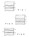
- reference numeral 1 denotes a substrate; 2, a metal layer; and 3, an aluminum layer.
- reference numeral 4 denotes an anodized film.
- a structure Fig. 2 in which an aluminum layer is partly anodized to form an anodized film on the aluminum layer or a structure (Fig. 3) in which an aluminum layer is completely anodized is obtained.
- a 0.3- ⁇ m thick Ni film was formed on a 0.8-mm thick cold-rolled steel plate 1 by arc discharge type ion plating to form a metal layer 2. 10- ⁇ m thick Al was deposited on the metal layer 2 by vacuum deposition to form an aluminum layer 3.
- the plated substrate prepared as described above was anodized in a sulfuric acid bath under conditions indicated below to form a porous anodized film 4.
- Electrolytic Bath Composition 15 wt% aqueous solution of sulfuric acid
- Electrolytic Bath Temperature 20°C Current Density: 1 to 3
- Electrolysis Time 10 to 30 minutes
- Anodized Film Thickness 5 to 10 ⁇ m
- a solid line represents changes in current of Example 1.
- a broken line represents changes in current density in anodizing following the same procedures as in Example 1 in a comparative example using a plating material having an Al layer formed on a substrate following the same procedures as in Example 1 except that a metal layer was not formed.
- the current density was decreased to 1/2 after about 30 minutes. This indicates that anodizing of the aluminum layer 3 has progressed and the Ni metal layer 2 was exposed. That is to say, it indicates that a uniform anodized film which reached the Ni layer after Al anodizing is obtained.
- the end time was determined to be a timing at which the current was reduced to 1/2.
- the comparative example indicated by the broken line close to the end of the electrolysis time, the current density largely varies. This indicates that the substrate is locally dissolved. The current is not greatly reduced because the cold-rolled steel plate is used as the substrate.
- Coloring of the anodized film was performed by using the following electrolytic coloring bath: Electrolytic Bath Composition: 20 g/l, CoSO4 25 g/l, H3BO3 15 g/l, (NH4)2SO4 Electrolytic Condition: 15 V (AC), 3 minutes
- Example 2 (not part of the present invention).
- Ni-Zn alloy Ni: 18 wt%; Zn: 82 wt%) film was formed on a 0.8-mm thick cold-rolled steel plate 1 by electroplating to obtain a metal layer 2.
- 15- ⁇ m thick Al was deposited on the metal layer 2 by vacuum deposition to form an aluminum layer 3.
- the resultant substrate was anodized in an oxalic acid bath under the conditions indicated below to form a porous film 4.
- Electrolytic Bath Composition 27 g/l, (COOH)2
- Electrolytic Bath Temperature 20°C Current Density: 1 to 3
- Electrolysis Time 10 to 30 minutes
- Anodized Film Tkickness 5 to ⁇ m
- a solid line represents changes in current of Example 2.
- a broken line represents changes in current in anodizing following the same procedures as in Example 2 in a comparative example using a plating material having an Al layer formed on a substrate following the same procedures as in Example 2 except that a metal layer was not formed.
- a current density was decreased to 1/2 after about 25 minutes. This indicates that anodizing of the aluminum layer 3 has progressed and the Ni-Zn alloy was exposed. That is to say, it indicates that a uniform anodized film which reached the Ni-Zn alloy layer after Al anodizing is obtained.
- the current density close to the end of the electrolysis time, the current density largely varies. This indicates that the substrate is locally dissolved. The current is not greatly reduced because the cold-rolled steel plate is used as the substrate.
- the resultant porous film 4 had a Vicker's hardness (HV) value of 550 and was found to be an anodized film having excellent antiwear properties.
- HV Vicker's hardness
- Ni, Ti, Ni-Zn, and Ni-Ti are exemplified as the materials for the metal layers.
- a material for the metal layer may be any material which is electrochemically nobler than the material of the aluminum layer and chemically stable.
- Nb, Ta, or W, or its alloy with Fe, P, Mn or Cu may be used to obtain the same effect as in the above examples.
Landscapes
- Chemical & Material Sciences (AREA)
- Chemical Kinetics & Catalysis (AREA)
- Engineering & Computer Science (AREA)
- Materials Engineering (AREA)
- Metallurgy (AREA)
- Organic Chemistry (AREA)
- Mechanical Engineering (AREA)
- Electrochemistry (AREA)
- Other Surface Treatments For Metallic Materials (AREA)
- Electroplating Methods And Accessories (AREA)
- Physical Vapour Deposition (AREA)
Claims (25)
- Matériau à plaquage d'aluminium pour anodisation comprenant :- un substrat (1) qui est constitué par l'un des acier et acier inoxydable ;- une couche d'aluminium (3) qui sert de couche la plus externe constituée par l'aluminium ou un alliage d'aluminium ; et- une couche de métal (2) comprise entre le substrat et la couche d'aluminium, la couche de métal étant électrochimiquement plus noble que la couche d'aluminium et chimiquement stable, et la couche de métal présentant une épaisseur de 0,3 µm à 2 µm.
- Matériau conforme à la revendication 1, caractérisé en ce que la couche de métal est une couche choisie dans l'ensemble formé par :(1) une couche de métal contenant un composant choisi dans l'ensemble formé par Ti, Ni, Nb, Ta et W,(2) une couche de métal constituée par un alliage qui comporte au moins deux composants choisis dans l'ensemble formé par Ti, Ni, Nb, Ta et W, ou(3) une couche de métal constituée par un alliage qui comporte au moins un composant choisi dans l'ensemble formé par Ti, Ni, Nb, Ta et W, et au moins un composant choisi dans l'ensemble formé par Zn, Fe, P, Mn et Cu.
- Matériau conforme à la revendication 1, caractérisé en ce que la couche de métal est au moins une couche comportant un composant choisi dans l'ensemble formé par Ti, Ni, Nb, Ta et W, et la couche d'aluminium a une épaisseur de 0,1 µm à 30 µm.
- Matériau conforme à la revendication 1, caractérisé en ce que la couche de métal est au moins une couche comportant deux composants choisis dans l'ensemble formé par Ti, Ni, Nb, Ta et W, et la couche d'aluminium a une épaisseur de 0,1 µm à 30 µm.
- Matériau conforme à la revendication 1, caractérisé en ce que la couche de métal est au moins une couche comportant un composant choisi dans l'ensemble formé par Ti, Ni, Nb, Ta et W, et un composant choisi dans l'ensemble formé par Zn, Fe, P, Mn et Cu, et
la couche d'aluminium a une épaisseur de 0,1 µm à 30 µm. - Matériau conforme à la revendication 1, caractérisé en ce que le substrat est constitué d'une des plaque en acier laminée à froid et plaque en acier inoxydable.
- Procédé d'anodisation d'un matériau à plaquage d'aluminium, caractérisé en ce qu'il comprend les étapes de :- préparation d'un substrat (1) qui est constitué par l'un des acier et acier inoxydable ;- formation d'au moins une couche de métal (2) qui est électrochimiquement plus noble que l'aluminium ou un alliage d'aluminium et chimiquement stable, et la couche de métal a une épaisseur de 0,3 µm à 2 µm ;- formation d'une couche d'aluminium (3) en aluminium ou alliage d'aluminium sur le substrat, la couche d'aluminium constituant la couche la plus externe, et ainsi obtention d'un matériau à plaquage d'aluminium ; et- anodisation du matériau à plaquage d'aluminium.
- Procédé conforme à la revendication 7, caractérisé en ce que le film d'aluminium a une épaisseur se situant dans l'intervalle allant de 0,1 µm à 30 µm.
- Procédé conforme à la revendication 7, caractérisé en ce que la couche de métal est une couche choisie dans l'ensemble formé par :(1) une couche de métal contenant un composant choisi dans l'ensemble formé par Ti, Ni, Nb, Ta et W,(2) une couche de métal constituée par un alliage qui comporte au moins deux composants choisis dans l'ensemble formé par Ti, Ni, Nb, Ta et W, et(3) une couche de métal constituée par un alliage qui comporte au moins un composant choisi dans l'ensemble formé par Ti, Ni, Nb, Ta et W, et au moins un composant choisi dans l'ensemble formé par Zn, Fe, P, Mn et Cu.
- Procédé conforme à la revendication 7, caractérisé en ce qu'il comprend les étapes de :- préparation du substrat ;- formation d'au moins une couche de métal sur une surface du substrat , la couche de métal comportant un composant choisi dans l'ensemble formé par Ti, Ni, Nb, Ta et W ;- formation d'une couche d'aluminium en aluminium ou alliage d'aluminium sur la couche de métal, la couche d'aluminium ayant une épaisseur de 0,1 µm à 30 µm et constituant la couche la plus externe, et ainsi obtention d'un matériau à plaquage d'aluminium et- anodisation du matériau à plaquage d'aluminium.
- Procédé conforme à la revendication 7, caractérisée en ce qu'il comprend les étapes de :- préparation du substrat ;- formation d'au moins une couche de métal sur une surface du substrat, la couche de métal comportant deux composants choisis dans l'ensemble formé par Ti, Ni, Nb, Ta et W ;- formation d'une couche d'aluminium en aluminium ou alliage d'aluminium sur la couche de métal, la couche d'aluminium ayant une épaisseur de 0,1 µm à 30 µm et constituant la couche la plus externe, et ainsi obtention d'un matériau à plaquage d'aluminium et- anodisation du matériau à plaquage d'aluminium.
- Procédé conforme à la revendication 7, caractérisé en ce qu'il comprend les étapes de :- préparation du substrat ;- formation d'au moins une couche de métal sur une surface du substrat, la couche de métal comportant un composant choisi dans l'ensemble formé par Ti, Ni, Nb, Ta et W, et au moins un composant choisi dans l'ensemble formé par Zn, Fe, P, Mn et Cu ;- formation d'une couche d'aluminium en aluminium ou alliage d'aluminium sur la couche de métal, la couche d'aluminium ayant une épaisseur de 0,1 µm à 30 µm et constituant la couche la plus externe, et ainsi obtention d'un matériau à plaquage d'aluminium et- anodisation du matériau à plaquage d'aluminium.
- Procédé conforme à la revendication 7, caractérisé en ce qu'il comprend en outre l'étape d'anodisation de la couche d'aluminium pour former un film anodisé et par la suite, l'étape de coloration du film anodisé.
- Matériau à plaquage d'aluminium anodisé comprenant :- un substrat (1) qui est constitué par l'un des acier et acier inoxydable ;- au moins une couche de métal (2) formée sur le substrat, la couche de métal étant électrochimiquement plus noble que l'aluminium ou alliage d'aluminium, et chimiquement stable ; et la couche de métal ayant une épaisseur de 0,3 µm à 2 µm ;- une couche d'aluminium (3) formé sur la couche de métal et constituée par l'aluminium ou un alliage d'aluminium ; et- une couche anodisée sous forme de film (4) formée sur la couche d'aluminium.
- Matériau conforme à la revendication 14, caractérisé en ce que l'épaisseur totale de la couche d'aluminium et de la couche anodisée sous forme de film se situe dans l'intervalle allant de 0,1 µm à 30 µm.
- Matériau conforme à la revendication 14, caractérisé en ce que la couche de métal est une couche choisie dans l'ensemble formé par(1) une couche de métal contenant un composant choisi dans l'ensemble formé par Ti, Ni, Nb, Ta et W,(2) une couche de métal constituée par un alliage qui comporte au moins deux composants choisis dans l'ensemble formé par Ti, Ni, Nb, Ta et W, et(3) une couche de métal constituée par un alliage qui comporte au moins un composant choisi dans l'ensemble formé par Ti, Ni, Nb, Ta et W, et au moins un composant choisi dans l'ensemble formé par Zn, Fe, P, Mn et Cu.
- Matériau conforme à la revendication 14, caractérisé en ce que la couche de métal est au moins une couche constituée par un composant choisi dans l'ensemble formé par Ti, Ni, Nb, Ta et W, et
l'épaisseur totale de la couche d'aluminium et de la couche anodisée sous forme de film se situe dans l'intervalle allant de 0,1 µm à 30 µm. - Matériau conforme à la revendication 14, caractérisé en ce que la couche de métal est au moins une couche constituée par deux composants choisis dans l'ensemble formé par Ti, Ni, Nb, Ta et W, et
l'épaisseur totale de la couche d'aluminium et de la couche anodisée sous forme de film se situe dans l'intervalle allant de 0,1 µm à 30 µm. - Matériau conforme à la revendication 14, caractérisé en ce que la couche de métal est au moins une couche comportant un composant choisi dans l'ensemble formé par Ti, Ni, Nb, Ta et W, et au moins un composant choisi dans l'ensemble formé par Zn, Fe, P, Mn et Cu, et
l'épaisseur totale de la couche d'aluminium et de la couche anodisée sous forme de film se situe dans l'intervalle allant de 0,1 µm à 30 µm. - Matériau à plaquage d'aluminium anodisé comprenant :- un substrat (1) qui est constitué par l'un des acier et acier inoxydable ;- au moins une couche de métal (2) formée sur le substrat, la couche de métal étant électrochimiquement plus noble que l'aluminium ou alliage d'aluminium, et chimiquement stable ; et la couche de métal ayant une épaisseur de 0,3 µm à 2 µm ; et- une couche anodisée sous forme de film (4) formée sur la couche de métal.
- Matériau conforme à la revendication 20, caractérisé en ce que la couche anodisée sous forme de film a une épaisseur se situant dans l'intervalle allant de 0,1 µm à 30 µm.
- Matériau conforme à la revendication 20, caractérisé en ce que la couche de métal est une couche choisie dans l'ensemble formé par :(1) une couche de métal contenant un composant choisi dans l'ensemble formé par Ti, Ni, Nb, Ta et W,(2) une couche de métal constituée par un alliage qui comporte au moins deux composants choisis dans l'ensemble formé par Ti, Ni, Nb, Ta et W, et(3) une couche de métal constituée par un alliage qui comporte au moins un composant choisi dans l'ensemble formé par Ti, Ni, Nb, Ta et W, et au moins un composant choisi dans l'ensemble formé par Zn, Fe, P, Mn et Cu.
- Matériau conforme à la revendication 20, caractérisé en ce que la couche de métal est au moins une couche constituée par un composant choisi dans l'ensemble formé par Ti, Ni, Nb, Ta et W, et
la couche anodisée sous forme de film a une épaisseur de 0,1 µm à 30 µm. - Matériau conforme à la revendication 20, caractérisé en ce que la couche de métal est au moins une couche constituée par deux composants choisis dans l'ensemble formé par Ti, Ni, Nb, Ta et W, et
la couche anodisée sous forme de film a une épaisseur de 0,1 µm à 30 µm. - Matériau conforme à la revendication 20, caractérisé en ce que la couche de métal est au moins une couche comportant un composant choisi dans l'ensemble formé par Ti, Ni, Nb, Ta et W, et au moins un composant choisi dans l'ensemble formé par Zn, Fe, P, Mn et Cu, et
la couche anodisée sous forme de film a une épaisseur de 0,1 µm à 30 µm.
Applications Claiming Priority (2)
| Application Number | Priority Date | Filing Date | Title |
|---|---|---|---|
| JP63210159A JPH0611917B2 (ja) | 1988-08-23 | 1988-08-23 | 陽極酸化処理用多層アルミニウムめっき基体 |
| JP210159/88 | 1988-08-23 |
Publications (2)
| Publication Number | Publication Date |
|---|---|
| EP0362535A1 EP0362535A1 (fr) | 1990-04-11 |
| EP0362535B1 true EP0362535B1 (fr) | 1996-05-15 |
Family
ID=16584741
Family Applications (1)
| Application Number | Title | Priority Date | Filing Date |
|---|---|---|---|
| EP89115486A Expired - Lifetime EP0362535B1 (fr) | 1988-08-23 | 1989-08-22 | Substance contenant un dépÔt d'aluminium pour l'anodisation |
Country Status (5)
| Country | Link |
|---|---|
| US (1) | US5002838A (fr) |
| EP (1) | EP0362535B1 (fr) |
| JP (1) | JPH0611917B2 (fr) |
| KR (1) | KR920000534B1 (fr) |
| DE (1) | DE68926485T2 (fr) |
Families Citing this family (19)
| Publication number | Priority date | Publication date | Assignee | Title |
|---|---|---|---|---|
| DE19726363A1 (de) * | 1997-06-21 | 1998-12-24 | Schaeffler Waelzlager Ohg | Verbundwerkstoff |
| JP3902883B2 (ja) * | 1998-03-27 | 2007-04-11 | キヤノン株式会社 | ナノ構造体及びその製造方法 |
| EP1099777A1 (fr) * | 1998-06-29 | 2001-05-16 | Kabushiki Kaisha Toshiba | Cible de vaporisation |
| DE10350190B4 (de) * | 2003-10-28 | 2005-11-10 | Federal-Mogul Nürnberg GmbH | Bauteil, insbesondere Kolben |
| JP4623977B2 (ja) * | 2004-02-17 | 2011-02-02 | 財団法人神奈川科学技術アカデミー | 陽極酸化ポーラスアルミナおよびその製造方法 |
| KR100672389B1 (ko) * | 2005-01-28 | 2007-01-24 | 엘지전자 주식회사 | 이동통신 단말기의 케이스 및 그 제작방법 |
| US20100162578A1 (en) * | 2008-12-29 | 2010-07-01 | Bennett Gregory T | Tools having anodized aluminum blades |
| CN102301040B (zh) | 2009-01-30 | 2014-10-15 | 夏普株式会社 | 模具和模具的制造方法、以及使用模具的防反射膜的制造方法 |
| JP5336417B2 (ja) * | 2010-04-27 | 2013-11-06 | 公益財団法人神奈川科学技術アカデミー | 陽極酸化ポーラスアルミナおよびその製造方法 |
| US8512872B2 (en) | 2010-05-19 | 2013-08-20 | Dupalectpa-CHN, LLC | Sealed anodic coatings |
| US8609254B2 (en) | 2010-05-19 | 2013-12-17 | Sanford Process Corporation | Microcrystalline anodic coatings and related methods therefor |
| KR101346014B1 (ko) * | 2012-04-12 | 2013-12-31 | 바코스 주식회사 | 금속 내외장재의 표면처리 방법 및 이에 의하여 제조된 표면구조를 가지는 금속 내외장재 |
| CN103628109A (zh) * | 2012-08-20 | 2014-03-12 | 叶宗嘉 | 阳极处理彩绘方法 |
| CN103898447A (zh) * | 2012-12-29 | 2014-07-02 | 深圳富泰宏精密工业有限公司 | 不锈钢表面处理方法及由该方法制得的外壳 |
| CN104309204B (zh) * | 2013-11-14 | 2017-05-31 | 比亚迪股份有限公司 | 一种钛或钛合金与树脂的复合体及其制备方法 |
| CN104309192B (zh) * | 2013-11-14 | 2017-05-31 | 比亚迪股份有限公司 | 一种不锈钢和树脂的复合体及其制备方法 |
| EP2832898A1 (fr) * | 2014-02-05 | 2015-02-04 | ThyssenKrupp Steel Europe AG | Composant enrichi par électrolyse à plasma et son procédé de fabrication |
| EP3778994A4 (fr) * | 2018-04-06 | 2021-12-22 | Furukawa Electric Co., Ltd. | Fil machine plaqué |
| JP7647050B2 (ja) * | 2020-10-02 | 2025-03-18 | スズキ株式会社 | 皮膜積層構造の製造方法および内燃機関用ピストン |
Family Cites Families (7)
| Publication number | Priority date | Publication date | Assignee | Title |
|---|---|---|---|---|
| US2443870A (en) * | 1944-01-26 | 1948-06-22 | Richard S Reynolds | Method of uniting laminations of aluminum and tin |
| US3090118A (en) * | 1959-04-16 | 1963-05-21 | Sunbeam Corp | Method of making a cooking vessel |
| US3489534A (en) * | 1967-01-03 | 1970-01-13 | Gen Electric | Lightweight metallic structure |
| SE7601702L (sv) * | 1975-04-18 | 1976-10-19 | Stauffer Chemical Co | Forfarande for pletering av metaller |
| FR2579999B1 (fr) * | 1985-04-03 | 1989-11-10 | Preci Coat Sa | Procede de traitment de surface d'une piece en alliages d'aluminium et piece en alliages d'aluminium obtenue par ce procede |
| US4681666A (en) * | 1986-11-13 | 1987-07-21 | Microelectronics And Computer Technology Corporation | Planarization of a layer of metal and anodic aluminum |
| JPH01237927A (ja) * | 1988-03-18 | 1989-09-22 | Hitachi Maxell Ltd | 磁気記録媒体および陽極酸化用材料 |
-
1988
- 1988-08-23 JP JP63210159A patent/JPH0611917B2/ja not_active Expired - Lifetime
-
1989
- 1989-08-14 US US07/393,806 patent/US5002838A/en not_active Expired - Fee Related
- 1989-08-19 KR KR1019890011842A patent/KR920000534B1/ko not_active Expired
- 1989-08-22 DE DE68926485T patent/DE68926485T2/de not_active Expired - Fee Related
- 1989-08-22 EP EP89115486A patent/EP0362535B1/fr not_active Expired - Lifetime
Also Published As
| Publication number | Publication date |
|---|---|
| KR900003421A (ko) | 1990-03-26 |
| DE68926485T2 (de) | 1996-12-05 |
| KR920000534B1 (ko) | 1992-01-14 |
| EP0362535A1 (fr) | 1990-04-11 |
| US5002838A (en) | 1991-03-26 |
| DE68926485D1 (de) | 1996-06-20 |
| JPH0257690A (ja) | 1990-02-27 |
| JPH0611917B2 (ja) | 1994-02-16 |
Similar Documents
| Publication | Publication Date | Title |
|---|---|---|
| EP0362535B1 (fr) | Substance contenant un dépÔt d'aluminium pour l'anodisation | |
| US4869971A (en) | Multilayer pulsed-current electrodeposition process | |
| US1947981A (en) | Plating aluminum | |
| EP0215950A1 (fr) | Procede de formation d'une pellicule composite d'aluminium | |
| US5322975A (en) | Universal carrier supported thin copper line | |
| EP3421646A1 (fr) | Procédé de coloration d'un élément en alliage d'aluminium | |
| JP7389847B2 (ja) | 軽合金上に薄い機能性コーティングを生成する方法 | |
| EP0389451A2 (fr) | Electrode durable pour utilisation en électrolyse et son procédé de production | |
| US4525759A (en) | Aluminum storage disc | |
| US3943039A (en) | Anodizing pretreatment for nickel plating | |
| JPH05503316A (ja) | 陽極酸化性金属基体に仕上げコーティングを被着する方法およびその製品 | |
| CA1138373A (fr) | Etamage electrolytique de l'acier suivi de refusion et d'electrolyse cathodique en bain alcalin | |
| US4632734A (en) | Process for electrochemically or chemically coating niobium | |
| Pushpavanam et al. | Rhodium—Electrodeposition and applications | |
| JP3180197B2 (ja) | アルミニウム及びアルミニウム合金の表面処理法 | |
| EP0095738B1 (fr) | Procédé pour fabriquer des tôles d'acier sans étain | |
| US4913973A (en) | Platinum-containing multilayer anode coating for low pH, high current density electrochemical process anodes | |
| Saubestre | Electroplating on Certain Transition Metals:(Groups IV, V, VI) | |
| JP3062062B2 (ja) | 電解用電極及びその製造方法 | |
| US4085013A (en) | Chromium plating process employing manganese dioxide coated anodes | |
| EP0215649B1 (fr) | Revêtement multiple d'anode de platine/ECA-1500 pour anodes destinées aux procédés électrochimiques à bas pH et à densité de courant élevée | |
| Vanden Berg | Electroplating Aluminium Alloys | |
| SU1691423A1 (ru) | Способ получени защитного покрыти на поверхности изделий | |
| EP0097759A1 (fr) | Formation d'une couche d'arrêt par anodisation sur les substrats d'aluminium et d'alliages d'aluminium | |
| SU796250A1 (ru) | Способ электролитического осаждени СЕРЕбРА HA МЕТАлличЕСКиЕ издЕли |
Legal Events
| Date | Code | Title | Description |
|---|---|---|---|
| PUAI | Public reference made under article 153(3) epc to a published international application that has entered the european phase |
Free format text: ORIGINAL CODE: 0009012 |
|
| 17P | Request for examination filed |
Effective date: 19890822 |
|
| AK | Designated contracting states |
Kind code of ref document: A1 Designated state(s): DE FR GB IT |
|
| 17Q | First examination report despatched |
Effective date: 19920414 |
|
| RBV | Designated contracting states (corrected) |
Designated state(s): DE GB |
|
| GRAH | Despatch of communication of intention to grant a patent |
Free format text: ORIGINAL CODE: EPIDOS IGRA |
|
| GRAA | (expected) grant |
Free format text: ORIGINAL CODE: 0009210 |
|
| AK | Designated contracting states |
Kind code of ref document: B1 Designated state(s): DE GB |
|
| REF | Corresponds to: |
Ref document number: 68926485 Country of ref document: DE Date of ref document: 19960620 |
|
| PLBE | No opposition filed within time limit |
Free format text: ORIGINAL CODE: 0009261 |
|
| STAA | Information on the status of an ep patent application or granted ep patent |
Free format text: STATUS: NO OPPOSITION FILED WITHIN TIME LIMIT |
|
| 26N | No opposition filed | ||
| PGFP | Annual fee paid to national office [announced via postgrant information from national office to epo] |
Ref country code: GB Payment date: 19970813 Year of fee payment: 9 |
|
| PGFP | Annual fee paid to national office [announced via postgrant information from national office to epo] |
Ref country code: DE Payment date: 19970925 Year of fee payment: 9 |
|
| PG25 | Lapsed in a contracting state [announced via postgrant information from national office to epo] |
Ref country code: GB Free format text: LAPSE BECAUSE OF NON-PAYMENT OF DUE FEES Effective date: 19980822 |
|
| GBPC | Gb: european patent ceased through non-payment of renewal fee |
Effective date: 19980822 |
|
| PG25 | Lapsed in a contracting state [announced via postgrant information from national office to epo] |
Ref country code: DE Free format text: LAPSE BECAUSE OF NON-PAYMENT OF DUE FEES Effective date: 19990601 |