EP0362797B1 - Procédé pour un fonctionnement économique en énergie de détecteurs de danger dans un dispositif de détection de danger - Google Patents
Procédé pour un fonctionnement économique en énergie de détecteurs de danger dans un dispositif de détection de danger Download PDFInfo
- Publication number
- EP0362797B1 EP0362797B1 EP89118338A EP89118338A EP0362797B1 EP 0362797 B1 EP0362797 B1 EP 0362797B1 EP 89118338 A EP89118338 A EP 89118338A EP 89118338 A EP89118338 A EP 89118338A EP 0362797 B1 EP0362797 B1 EP 0362797B1
- Authority
- EP
- European Patent Office
- Prior art keywords
- detector
- time
- voltage
- detectors
- microcomputer
- Prior art date
- Legal status (The legal status is an assumption and is not a legal conclusion. Google has not performed a legal analysis and makes no representation as to the accuracy of the status listed.)
- Expired - Lifetime
Links
Images
Classifications
-
- G—PHYSICS
- G08—SIGNALLING
- G08B—SIGNALLING SYSTEMS, e.g. PERSONAL CALLING SYSTEMS; ORDER TELEGRAPHS; ALARM SYSTEMS
- G08B26/00—Alarm systems in which substations are interrogated in succession by a central station
- G08B26/005—Alarm systems in which substations are interrogated in succession by a central station with substations connected in series, e.g. cascade
Definitions
- the invention relates to a method for energy-saving operation of hazard detectors in a hazard detection system according to the preamble of claim 1.
- Such a hazard detection system is known from DE-PS 25 33 382.
- the individual detectors are connected in a chain to the detection line.
- the measured values of the individual detectors are queried cyclically from the control center and sent to the central evaluation device in order to obtain differentiated fault or alarm messages from the analog values to be linked.
- all detectors are separated from the detection line by a voltage change and then switched on again in a predetermined order in such a way that each detector, after a time delay corresponding to its measured value, by means of a switching transistor arranged in one of the wires of the detection line, additionally the following detectors turns on.
- the respective detector address is derived from the number of previous increases in line current and the analog measured value from the length of the relevant switching delays.
- the detectors are operated from their energy stores during this time. After the query, the energy stores are recharged during the so-called rest period with increased line voltage.
- Hazard detectors increasingly require high-quality sensors and transmission technology. Instead of a collective address, individual addressing is required, as is the case with the hazard alarm system described above.
- Control commands can also be transmitted from the control center to the individual detectors, which are received by the individual detectors, as is already known from DE-PS 25 33 354.
- the data received and reported by the individual detectors can also be transmitted in the form of pulse telegrams within certain time windows.
- CMOS complementary metal-oxide-semiconductor
- special sensors e.g. to operate the measuring part of an optical scattered light smoke detector in a pulsed manner, as described in EP - 125 485 - AI.
- the possibility of completely or partially separating the necessary energy e.g. to be supplied via a separate line, which also increases the complexity and the costs of a hazard detection system.
- the object of the invention is to provide, while avoiding the disadvantages described above, a method for the energy-saving operation of hazard detectors in a hazard detection system, which allows a relatively simple and reliable switching on and off of a microcomputer.
- switching criteria are used for switching the microcomputer on and off in the respective detector, which are specific to a hazard detection system and already exist, i.e. which are used and designed in a special way for this.
- each detector receives a certain voltage (an activation voltage) which switches on the microcomputer, but only activates the detector after a predetermined start-up time. Then the data traffic takes place with the head office, i.e. the detector receives and sends (reports) signals. The microcomputer is then switched off by switching to the next detector.
- the connection voltage is expediently formed by the interrogation voltage.
- the method according to the invention modifies the known chain modulation in such a way that each detector initially remains inactive for a predetermined start-up time after the application of the interrogation voltage processes its data traffic with the control center in a certain reception time and response time and then switches through to the next detector.
- the microcomputer of each detector can start up with the specified start-up time. When switching to the next detector, the microcomputer is switched off again. The microcomputer is switched on for an optimally short time and consequently less energy is consumed on average.
- the start-up time for the microcomputer is obtained in a special way without having to provide a separate start-up time for each detector. All that is required is a first start-up time for the microcomputer of the first detector. After this start-up time, the first detector switches directly to the second detector. In the subsequent reception and transmission time of the first detector, the data communication between the first detector and the control center takes place. This reception and response time is also the start-up time for the microcomputer of the second detector. This process continues until the last detector. This procedure considerably reduces the time required and thus extends the available rest period in which the energy storage devices of the detectors are charged. This allows an increase in the sampling rate and / or an increased energy supply.
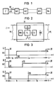
- a plurality of detectors M1 to Mn are connected to a central station Z here, for example, only on one reporting primary line ML.
- the line current IL flows on the signal line ML and the line voltage UL is present, which can be switched to different values (FIG. 1).
- the detector M shown in FIG. 2 has, in addition to the switching transistor T switched on in the one line of the detection line ML, the logic logic VL, which represents the heart of the detector and is formed by a microcomputer.
- the logic logic serves the actual sensor part.
- the logic logic VL is acted upon by the voltage measuring device MU, which monitors the line voltage UL and outputs switching signals to the logic logic VL in accordance with the line voltage applied.
- This logic logic causes signals to a control device ST and also signals for switching DS of the switching transistor T so that the following detector is connected to the line voltage.
- Fig. 3 shows how the individual detectors are switched on in sequence.
- the line voltage UL is plotted against the time t for the detectors M1 to M3.
- the rest voltage UR is present on the detection line ML.
- An interrogation cycle then begins with the separation of the line from the line voltage UL, i.e. the starting voltage US, which is preferably equal to zero, is applied for the starting time ts.
- the interrogation voltage UA is preferably below the value of the quiescent voltage UR. It is shown for the detector M2 that it only receives the interrogation voltage UA after the DS of the first detector M1 has been switched through. The same applies to detector M3.
- the data transmission to the detector is generally done by modulating the line voltage UL in the control center, while data transmission to the control center is done by modulating the line current IL in the detector.
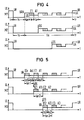
- FIG. 4 shows the profile of the line voltage UL over time t at the input of the detectors M1, M2 and M3.
- the open circuit voltage UR is applied for the rest time tr.
- the application of the interrogation voltage UA which is also the switch-on voltage UAN for the microcomputer, is applied to the first detector, which is activated after the start-up time tan and thus receives receive signals E1 from the control center for the receive time te and then response signals A1 in time Ta can report to the headquarters.
- the detector M1 then switches to detector M2 through (DS).
- the detector M2 is in turn activated within the start-up time tan and then begins data traffic to the control center.
- the third detector is then switched through. If the primary signal line ML is queried, the open circuit voltage UR is applied to the signal line. With the respective switching through DS to the next detector, the microcomputer of the detector in question is switched off again, so that the microcomputer only requires energy for an optimally short time.
- Fig. 5 is a voltage diagram for three detectors, another embodiment of the Invention according to the procedure. All that is required is a single start-up time for all detectors on a line, which advantageously reduces the polling time per detector. This can increase the number of detectors that can be connected and / or speed up the query. In any case, the respective microcomputer is only switched on for a short time. When the interrogation voltage UA is applied, the microcomputer of the first detector starts up. During this time, the detector receives received signals EO from the control center and could then report an AO response to the control center. Neither is possible because the microcomputer is still starting up and is therefore not functional.
- the functionality is only awakened during the response time ta0, so that the first detector can receive and process the receive signal E1 intended for it only after this start-up time tan1.
- detector M1 switches through to detector M2 (DS).
- the start-up time tan2 runs for the second detector M2, which then switches through to the third detector M3 (DS) as soon as it receives the data E2 from the control center.
- each detector switches through to the next detector immediately upon receipt of the first signals from the control center . This process is repeated in the same way for the other detectors on the line, until after the last detector has been processed, the line is again connected to the rest voltage.
- the received signals can be carried out in part with the voltage level which corresponds to the quiescent voltage, as a result of which the time required for energy supply is advantageously shortened and the number of detectors that can be connected is increased and / or the query is accelerated.
Landscapes
- Business, Economics & Management (AREA)
- Emergency Management (AREA)
- Physics & Mathematics (AREA)
- General Physics & Mathematics (AREA)
- Alarm Systems (AREA)
- Emergency Alarm Devices (AREA)
Claims (4)
caractérisé par le fait
que lors de l'interrogation cyclique successive, chaque transmetteur (Mn) reçoit une tension déterminée (tension de raccordement UAN), qui active le micro-ordinateur, mais active le transmetteur considéré, uniquement après une durée de démarrage prédéterminée (tan) du transmetteur considéré, qu'après l'écoulement de la durée de démarrage (tan), il se produit un trafic d'échange de données avec le central (Z), auquel cas pour la réception (E1.E2,...), il est prévu respectivement un temps de réponse déterminé (te) et, pour la réponse (signalisation) (A1,A2,...), il est prévu respectivement un temps de réponse déterminé (te), et qu'ensuite, le micro-ordinateur est débranché lors de l'interconnexion (DS) établie avec le transmetteur immédiatement suivant.
Applications Claiming Priority (2)
| Application Number | Priority Date | Filing Date | Title |
|---|---|---|---|
| DE3834043 | 1988-10-06 | ||
| DE3834043 | 1988-10-06 |
Publications (4)
| Publication Number | Publication Date |
|---|---|
| EP0362797A2 EP0362797A2 (fr) | 1990-04-11 |
| EP0362797A3 EP0362797A3 (fr) | 1991-01-16 |
| EP0362797B1 true EP0362797B1 (fr) | 1994-12-28 |
| EP0362797B2 EP0362797B2 (fr) | 2000-05-17 |
Family
ID=6364534
Family Applications (1)
| Application Number | Title | Priority Date | Filing Date |
|---|---|---|---|
| EP89118338A Expired - Lifetime EP0362797B2 (fr) | 1988-10-06 | 1989-10-03 | Procédé pour un fonctionnement économique en énergie de détecteurs de danger dans un dispositif de détection de danger |
Country Status (3)
| Country | Link |
|---|---|
| EP (1) | EP0362797B2 (fr) |
| AT (1) | ATE116464T1 (fr) |
| DE (1) | DE58908831D1 (fr) |
Families Citing this family (3)
| Publication number | Priority date | Publication date | Assignee | Title |
|---|---|---|---|---|
| DE4030298A1 (de) * | 1990-09-25 | 1992-03-26 | Siemens Ag | Gefahrenmeldeanlage |
| DE102009050692B4 (de) * | 2009-10-26 | 2011-12-01 | Phoenix Contact Gmbh & Co. Kg | Sicherheits-Kommunikationssystem zur Signalisierung von Systemzuständen |
| DE102011018630B4 (de) * | 2011-04-21 | 2013-02-07 | Phoenix Contact Gmbh & Co. Kg | Sicherheits-Kommunikationssystem zur Signalisierung von Systemzuständen |
Family Cites Families (3)
| Publication number | Priority date | Publication date | Assignee | Title |
|---|---|---|---|---|
| GB2131991B (en) * | 1982-11-12 | 1986-05-29 | Robert Philp | Telemetry and like signaling systems |
| DE3313137A1 (de) * | 1983-04-12 | 1984-10-18 | Siemens AG, 1000 Berlin und 8000 München | Schaltungsanordnung zur stoersignalunterdrueckung in optischen rauchmeldern |
| KR910008738B1 (ko) * | 1987-02-20 | 1991-10-19 | 닛본 덴기 가부시기가이샤 | 밧데리 절약 채널 스캔 기능을 갖고 있는 휴대용 무선 송수신기 |
-
1989
- 1989-10-03 AT AT89118338T patent/ATE116464T1/de not_active IP Right Cessation
- 1989-10-03 DE DE58908831T patent/DE58908831D1/de not_active Expired - Fee Related
- 1989-10-03 EP EP89118338A patent/EP0362797B2/fr not_active Expired - Lifetime
Also Published As
| Publication number | Publication date |
|---|---|
| EP0362797A3 (fr) | 1991-01-16 |
| EP0362797A2 (fr) | 1990-04-11 |
| ATE116464T1 (de) | 1995-01-15 |
| EP0362797B2 (fr) | 2000-05-17 |
| DE58908831D1 (de) | 1995-02-09 |
Similar Documents
| Publication | Publication Date | Title |
|---|---|---|
| EP1206765B1 (fr) | Procede et dispositif d'affectation automatique d'adresses de detecteurs dans un systeme avertisseur de danger | |
| DE68924615T2 (de) | Überwachungssystem für Funkkommunikationsapparate. | |
| EP0067339B1 (fr) | Méthode et arrangement pour détecter des perturbations dans des systèmes de signalisation de risques, en particulier signalisation d'incendie | |
| WO2011032977A1 (fr) | Procédé et dispositif pour activer des dispositifs utilisateurs d'un système de bus et dispositif utilisateur correspondant | |
| DE2533354C3 (de) | Einrichtung zum Übertragen von Steuerbefehlen in einem Brandschutzsystem | |
| DE2533330B2 (de) | Verfahren und einrichtung zur uebertragung von messwerten in einem brandmeldesystem | |
| DE3249787C2 (fr) | ||
| DE3623705C2 (fr) | ||
| EP0362797B2 (fr) | Procédé pour un fonctionnement économique en énergie de détecteurs de danger dans un dispositif de détection de danger | |
| DE3150313C2 (de) | Anordnung zur Ermittlung und Rückmeldung der Stellung einer Reihe von Schaltern und zur Überwachung der Verbindungsleitung | |
| EP0362798B1 (fr) | Procédé pour un fonctionnement économique en énergie de détecteurs de danger dans un dispositif de détection de danger | |
| DE10342625A1 (de) | Sensor | |
| DE2456630C3 (de) | Fernsteueranlage | |
| DE3614692C2 (fr) | ||
| DE3424294A1 (de) | Abfrageeinrichtung zur identifikation der stellung von schaltern | |
| CH661136A5 (de) | Brand- oder einbruchmeldeanlage. | |
| EP0212106B1 (fr) | Méthode de transmission de valeurs de mesure | |
| DE3225032C2 (de) | Verfahren und Einrichtung zur wahlweisen automatischen Abfrage der Melderkennung oder des Meldermeßwerts in einer Gefahrenmeldeanlage | |
| DE2853147C2 (de) | Datenein- und -ausgabeanordnung | |
| EP2515553B1 (fr) | Système de communication de sécurité destiné à la signalisation d'états du système | |
| EP0510354B1 (fr) | Méthode de surveillance du fonctionnement d'un coupleur de bus | |
| DE3022058C2 (de) | Einrichtung zur signaltechnisch sicheren Steuerung eines Schaltgliedes | |
| DE4113966C2 (fr) | ||
| DE859779C (de) | Schaltungsanordnung zur Fernmeldung von Betriebszustaenden | |
| EP0178474A2 (fr) | Procédé et dispositif pour l'identification du détecteur d'un système détecteur de dangers |
Legal Events
| Date | Code | Title | Description |
|---|---|---|---|
| PUAI | Public reference made under article 153(3) epc to a published international application that has entered the european phase |
Free format text: ORIGINAL CODE: 0009012 |
|
| AK | Designated contracting states |
Kind code of ref document: A2 Designated state(s): AT BE CH DE FR GB IT LI LU NL SE |
|
| PUAL | Search report despatched |
Free format text: ORIGINAL CODE: 0009013 |
|
| AK | Designated contracting states |
Kind code of ref document: A3 Designated state(s): AT BE CH DE FR GB IT LI LU NL SE |
|
| 17P | Request for examination filed |
Effective date: 19901205 |
|
| 17Q | First examination report despatched |
Effective date: 19931105 |
|
| GRAA | (expected) grant |
Free format text: ORIGINAL CODE: 0009210 |
|
| AK | Designated contracting states |
Kind code of ref document: B1 Designated state(s): AT BE CH DE FR GB IT LI LU NL SE |
|
| REF | Corresponds to: |
Ref document number: 116464 Country of ref document: AT Date of ref document: 19950115 Kind code of ref document: T |
|
| REF | Corresponds to: |
Ref document number: 58908831 Country of ref document: DE Date of ref document: 19950209 |
|
| ITF | It: translation for a ep patent filed | ||
| ET | Fr: translation filed | ||
| GBT | Gb: translation of ep patent filed (gb section 77(6)(a)/1977) |
Effective date: 19950303 |
|
| PLBI | Opposition filed |
Free format text: ORIGINAL CODE: 0009260 |
|
| 26 | Opposition filed |
Opponent name: PREUSSAG AG Effective date: 19950926 |
|
| NLR1 | Nl: opposition has been filed with the epo |
Opponent name: PREUSSAG AG |
|
| PLBF | Reply of patent proprietor to notice(s) of opposition |
Free format text: ORIGINAL CODE: EPIDOS OBSO |
|
| PGFP | Annual fee paid to national office [announced via postgrant information from national office to epo] |
Ref country code: LU Payment date: 19971013 Year of fee payment: 9 |
|
| PG25 | Lapsed in a contracting state [announced via postgrant information from national office to epo] |
Ref country code: LU Free format text: LAPSE BECAUSE OF NON-PAYMENT OF DUE FEES Effective date: 19981003 |
|
| PLAW | Interlocutory decision in opposition |
Free format text: ORIGINAL CODE: EPIDOS IDOP |
|
| PLAW | Interlocutory decision in opposition |
Free format text: ORIGINAL CODE: EPIDOS IDOP |
|
| PUAH | Patent maintained in amended form |
Free format text: ORIGINAL CODE: 0009272 |
|
| STAA | Information on the status of an ep patent application or granted ep patent |
Free format text: STATUS: PATENT MAINTAINED AS AMENDED |
|
| 27A | Patent maintained in amended form |
Effective date: 20000517 |
|
| AK | Designated contracting states |
Kind code of ref document: B2 Designated state(s): AT BE CH DE FR GB IT LI LU NL SE |
|
| REG | Reference to a national code |
Ref country code: CH Ref legal event code: AEN Free format text: AUFRECHTERHALTUNG DES PATENTES IN GEAENDERTER FORM |
|
| NLR2 | Nl: decision of opposition | ||
| ITF | It: translation for a ep patent filed | ||
| GBTA | Gb: translation of amended ep patent filed (gb section 77(6)(b)/1977) | ||
| ET3 | Fr: translation filed ** decision concerning opposition | ||
| NLR3 | Nl: receipt of modified translations in the netherlands language after an opposition procedure | ||
| REG | Reference to a national code |
Ref country code: GB Ref legal event code: IF02 |
|
| PGFP | Annual fee paid to national office [announced via postgrant information from national office to epo] |
Ref country code: AT Payment date: 20021004 Year of fee payment: 14 |
|
| PGFP | Annual fee paid to national office [announced via postgrant information from national office to epo] |
Ref country code: GB Payment date: 20021010 Year of fee payment: 14 |
|
| PGFP | Annual fee paid to national office [announced via postgrant information from national office to epo] |
Ref country code: SE Payment date: 20021016 Year of fee payment: 14 |
|
| PGFP | Annual fee paid to national office [announced via postgrant information from national office to epo] |
Ref country code: NL Payment date: 20021021 Year of fee payment: 14 Ref country code: BE Payment date: 20021021 Year of fee payment: 14 |
|
| PGFP | Annual fee paid to national office [announced via postgrant information from national office to epo] |
Ref country code: FR Payment date: 20021023 Year of fee payment: 14 |
|
| PGFP | Annual fee paid to national office [announced via postgrant information from national office to epo] |
Ref country code: DE Payment date: 20021216 Year of fee payment: 14 |
|
| PGFP | Annual fee paid to national office [announced via postgrant information from national office to epo] |
Ref country code: CH Payment date: 20030115 Year of fee payment: 14 |
|
| PG25 | Lapsed in a contracting state [announced via postgrant information from national office to epo] |
Ref country code: GB Free format text: LAPSE BECAUSE OF NON-PAYMENT OF DUE FEES Effective date: 20031003 Ref country code: AT Free format text: LAPSE BECAUSE OF NON-PAYMENT OF DUE FEES Effective date: 20031003 |
|
| PG25 | Lapsed in a contracting state [announced via postgrant information from national office to epo] |
Ref country code: SE Free format text: LAPSE BECAUSE OF NON-PAYMENT OF DUE FEES Effective date: 20031004 |
|
| PG25 | Lapsed in a contracting state [announced via postgrant information from national office to epo] |
Ref country code: LI Free format text: LAPSE BECAUSE OF NON-PAYMENT OF DUE FEES Effective date: 20031031 Ref country code: CH Free format text: LAPSE BECAUSE OF NON-PAYMENT OF DUE FEES Effective date: 20031031 Ref country code: BE Free format text: LAPSE BECAUSE OF NON-PAYMENT OF DUE FEES Effective date: 20031031 |
|
| BERE | Be: lapsed |
Owner name: *SIEMENS A.G. Effective date: 20031031 |
|
| PG25 | Lapsed in a contracting state [announced via postgrant information from national office to epo] |
Ref country code: NL Free format text: LAPSE BECAUSE OF NON-PAYMENT OF DUE FEES Effective date: 20040501 Ref country code: DE Free format text: LAPSE BECAUSE OF NON-PAYMENT OF DUE FEES Effective date: 20040501 |
|
| GBPC | Gb: european patent ceased through non-payment of renewal fee |
Effective date: 20031003 |
|
| EUG | Se: european patent has lapsed | ||
| REG | Reference to a national code |
Ref country code: CH Ref legal event code: PL |
|
| PG25 | Lapsed in a contracting state [announced via postgrant information from national office to epo] |
Ref country code: FR Free format text: LAPSE BECAUSE OF NON-PAYMENT OF DUE FEES Effective date: 20040630 |
|
| NLV4 | Nl: lapsed or anulled due to non-payment of the annual fee |
Effective date: 20040501 |
|
| REG | Reference to a national code |
Ref country code: FR Ref legal event code: ST |
|
| PG25 | Lapsed in a contracting state [announced via postgrant information from national office to epo] |
Ref country code: IT Free format text: LAPSE BECAUSE OF NON-PAYMENT OF DUE FEES;WARNING: LAPSES OF ITALIAN PATENTS WITH EFFECTIVE DATE BEFORE 2007 MAY HAVE OCCURRED AT ANY TIME BEFORE 2007. THE CORRECT EFFECTIVE DATE MAY BE DIFFERENT FROM THE ONE RECORDED. Effective date: 20051003 |