EP0362935A2 - Transresistanzvorrichtung mit Drain-Vorspannung - Google Patents
Transresistanzvorrichtung mit Drain-Vorspannung Download PDFInfo
- Publication number
- EP0362935A2 EP0362935A2 EP89202433A EP89202433A EP0362935A2 EP 0362935 A2 EP0362935 A2 EP 0362935A2 EP 89202433 A EP89202433 A EP 89202433A EP 89202433 A EP89202433 A EP 89202433A EP 0362935 A2 EP0362935 A2 EP 0362935A2
- Authority
- EP
- European Patent Office
- Prior art keywords
- transistors
- output terminals
- terminals
- output
- input
- Prior art date
- Legal status (The legal status is an assumption and is not a legal conclusion. Google has not performed a legal analysis and makes no representation as to the accuracy of the status listed.)
- Granted
Links
- 239000003990 capacitor Substances 0.000 claims description 25
- 230000008878 coupling Effects 0.000 claims description 6
- 238000010168 coupling process Methods 0.000 claims description 6
- 238000005859 coupling reaction Methods 0.000 claims description 6
- 230000001276 controlling effect Effects 0.000 abstract 1
- 238000000034 method Methods 0.000 description 16
- 238000012545 processing Methods 0.000 description 12
- 238000009499 grossing Methods 0.000 description 7
- 238000013459 approach Methods 0.000 description 5
- 230000004044 response Effects 0.000 description 4
- 239000004065 semiconductor Substances 0.000 description 4
- 238000012546 transfer Methods 0.000 description 3
- 238000001914 filtration Methods 0.000 description 2
- 238000012986 modification Methods 0.000 description 2
- 230000004048 modification Effects 0.000 description 2
- 230000008569 process Effects 0.000 description 2
- 238000005070 sampling Methods 0.000 description 2
- 230000009471 action Effects 0.000 description 1
- 230000005540 biological transmission Effects 0.000 description 1
- 230000015572 biosynthetic process Effects 0.000 description 1
- 230000015556 catabolic process Effects 0.000 description 1
- 238000006243 chemical reaction Methods 0.000 description 1
- 229940000425 combination drug Drugs 0.000 description 1
- 239000013078 crystal Substances 0.000 description 1
- 238000006731 degradation reaction Methods 0.000 description 1
- 230000000593 degrading effect Effects 0.000 description 1
- 230000001934 delay Effects 0.000 description 1
- 238000013461 design Methods 0.000 description 1
- 238000011161 development Methods 0.000 description 1
- 230000009977 dual effect Effects 0.000 description 1
- 230000000694 effects Effects 0.000 description 1
- 238000005516 engineering process Methods 0.000 description 1
- 238000002347 injection Methods 0.000 description 1
- 239000007924 injection Substances 0.000 description 1
- 238000007689 inspection Methods 0.000 description 1
- 230000010354 integration Effects 0.000 description 1
- QHGVXILFMXYDRS-UHFFFAOYSA-N pyraclofos Chemical compound C1=C(OP(=O)(OCC)SCCC)C=NN1C1=CC=C(Cl)C=C1 QHGVXILFMXYDRS-UHFFFAOYSA-N 0.000 description 1
- 239000010453 quartz Substances 0.000 description 1
- VYPSYNLAJGMNEJ-UHFFFAOYSA-N silicon dioxide Inorganic materials O=[Si]=O VYPSYNLAJGMNEJ-UHFFFAOYSA-N 0.000 description 1
- 239000007787 solid Substances 0.000 description 1
- 239000000243 solution Substances 0.000 description 1
- 238000003786 synthesis reaction Methods 0.000 description 1
Images


Classifications
-
- H—ELECTRICITY
- H03—ELECTRONIC CIRCUITRY
- H03H—IMPEDANCE NETWORKS, e.g. RESONANT CIRCUITS; RESONATORS
- H03H7/00—Multiple-port networks comprising only passive electrical elements as network components
-
- H—ELECTRICITY
- H03—ELECTRONIC CIRCUITRY
- H03F—AMPLIFIERS
- H03F1/00—Details of amplifiers with only discharge tubes, only semiconductor devices or only unspecified devices as amplifying elements
- H03F1/56—Modifications of input or output impedances, not otherwise provided for
-
- H—ELECTRICITY
- H03—ELECTRONIC CIRCUITRY
- H03F—AMPLIFIERS
- H03F3/00—Amplifiers with only discharge tubes or only semiconductor devices as amplifying elements
- H03F3/45—Differential amplifiers
- H03F3/45071—Differential amplifiers with semiconductor devices only
- H03F3/45076—Differential amplifiers with semiconductor devices only characterised by the way of implementation of the active amplifying circuit in the differential amplifier
- H03F3/45475—Differential amplifiers with semiconductor devices only characterised by the way of implementation of the active amplifying circuit in the differential amplifier using IC blocks as the active amplifying circuit
-
- H—ELECTRICITY
- H03—ELECTRONIC CIRCUITRY
- H03H—IMPEDANCE NETWORKS, e.g. RESONANT CIRCUITS; RESONATORS
- H03H11/00—Networks using active elements
- H03H11/02—Multiple-port networks
- H03H11/04—Frequency selective two-port networks
-
- H—ELECTRICITY
- H03—ELECTRONIC CIRCUITRY
- H03H—IMPEDANCE NETWORKS, e.g. RESONANT CIRCUITS; RESONATORS
- H03H11/00—Networks using active elements
- H03H11/02—Multiple-port networks
- H03H11/04—Frequency selective two-port networks
- H03H11/12—Frequency selective two-port networks using amplifiers with feedback
- H03H11/1291—Current or voltage controlled filters
-
- H—ELECTRICITY
- H03—ELECTRONIC CIRCUITRY
- H03H—IMPEDANCE NETWORKS, e.g. RESONANT CIRCUITS; RESONATORS
- H03H11/00—Networks using active elements
- H03H11/02—Multiple-port networks
- H03H11/24—Frequency-independent attenuators
Definitions
- This invention relates to a tunable resistance device useful for implementing various analog signal processing functions and, especially, to a drain-biassed transresistance device in an active continuous time filter which provides the filter with a tunable frequency response.
- this invention relates to a device comprising: first and second MOS transistors each having a drain electrode and a gate electrode, a differential amplifier having output means and first and second inputs coupled to the drain electrodes of the first and second transistors, respectively, a feedback circuit coupling said output means of said differential amplifier to at least one of the inputs of the differential amplifier.
- RC time constants In the field of analog signal processing it is important to be able to monolithically generate RC time constants that are accurate, stable and controllable despite variations in process conditions and variations in temperature.
- the RC time constants determine crucial values such as timing delays and filter frequencies.
- Accurate RC time constants have been implemented monolithically in VLSI compatible switching technologies such as charge-coupled devices (CCD) and switched-capacitor filters by means of the controlled sampling and transfer of charge packages at a precise clock frequency (f ck ).
- CCD charge-coupled devices
- switched-capacitor filters In the switched-capacitor technique the resistance (R) is generated by data sampling and RC can be made to track a fixed clock frequency (l/f ck ).
- the switched-capacitor technique has become popular in the MOS analog signal processing field, especially in the development of monolithic filters.
- One reason for this is that the RC time constants of the basic filter building blocks, such as integrators, can be accurately controlled over varying process and temperatures ranges.
- the switched-capaci lengthytor technique suffers from a number of drawbacks including, for example, noise folding back into the baseband, the need for antialiasing and smoothing filters, charge injection by the switches, and the presence of switching noise. These drawbacks become more significant as the signal frequency is increased.
- One solution to the problem of providing a linear tunable resistor element with good frequency performance is to use a MOS transistor as a voltage controlled resistor.
- MOS transistor By operating a pair of such transistors (M1 & M2) differentially the second order nonlinear terms in the integrator function can be cancelled.
- the gate voltage is used to tune or vary the value of R until the correct RC constant is achieved.
- Another object of the invention is to use a non-linear MOS device in a novel manner so as to achieve a device with a wide range of continuous linear resistance (R).
- a further object of the invention is to provide an electronically controllable MOS transistor device whose resistance R is variable in a continuous and linear manner over a wide dynamic range so as to provide good high frequency characteristics, direct on-chip tuning, high input impedance and good linearity over a wide input range.
- a still further object of the invention is to provide a new method for generating accurate and controllable RC values for implementing various analog signal processing functions, e.g. filtering.
- Another object of the invention is to provide a family of unique building blocks suitable for high frequency continuous time filters which exhibit a high input impedance to the applied signals.
- a further object of the invention is to provide a high frequency continuous time filter that can be entirely integrated onto a single semiconductor chip.
- Still another object of the invention is to provide an RC building block in which the value of RC automatically tracks clock frequency without the use of phase-locked-loop.
- a device of the type set forth in the preamble is characterized in that the device further comprises: first and second adjustable bias current sources, means connecting said first current source and said first transistor in series circuit across terminals of a source of supply voltage and with a drain electrode connected to the first current source, means connecting said second current source and said second transistor in series circuit across the terminals of the source of supply voltage and with a drain electrode connected to the second current source, a pair of signal input terminals connected to respective gate electrodes of the first and second transistors, and means for adjusting the value of bias currents supplied by the bias current sources to said first and second transistors thereby to bias the transistors into their triode regions, adjustment of said bias current sources being operative to vary the bias currents and thereby the drain voltages ofthe transistors so as to linearly vary the effective resistance of said transistors.
- the foregoing and other objects and advantages of the invention are achieved by means of a drain-biassed transresistance MOS transistor device which makes use of the linear transresistance variation of a MOS transistor operated in the triode region.
- the input signal is applied to the gate of the MOS transistor and its effective resistance is tunable (adjustable) by controlling the transistor's drain voltage by means of an adjustable bias current applied thereto.
- the invention makes it possible to provide a family of elementary RC controllable devices suitable for avarious high frequency analog signal processing applications such as high frequency continuous time filter building blocks.
- a preferred embodiment of the invention uses a pair of matched MOS transistors connected in a common source configuration and biassed by two matched current sources coupled to respective drain electrodes of the pair of MOS transistors thereby to adjust the values of the drain voltages.
- the biasing of the drain voltages of the pair of matched MOS transistors into their triode regions provides a continuously variable linear resistance R created by the differential transresistance of the pair of MOS transistors.
- the drain voltages of the MOS transistors determine the resistance value R, which is controlled via a bias current (I B ) generated on the semiconductor chip by a bias current generator circuit.
- the bias current generator can be arranged so that the RC product is proportional to a clock frequency (e.g. 1/f ck ).
- the invention thus provides a new drain-biassed transresistance (DBT) device as an elementary building block for a wide variety of high frequency analog signal processing devices, such as VLSI-compatible continuous time analog filters (e.g. antialiasing filters or smoothing filters) modulator/ demodulator in data transmission apparatus and as a stereo decoder in an audio system.
- DBT filter can be used in applications that presently use switched-capacitor filters, e.g. speech analysis and synthesis, mobile transceivers, radar and sonar devices, orthogonal transforms, automatic inspection systems etc.
- novel DBT devices to be described provide good RC controllability and high frequency response, a large linear input range (about 2/3 of the supply voltage in one experimental device), high input impedance, ease of tuning, integration of entire video signal processing functions onto a single chip to cut costs and increase reliability, and the ability to make RC track l/f ck without using a phase-locked-loop.
- Figure 1 illustrates the basic elementary DBT tunable RC element suitable for use as the basic building block in high frequency continuous time filters and other high frequency analog signal processing devices.
- the circuit of Fig. 1 shows a single-ended version of the basic DBT element. It consists of a matched pair of MOS transistors M1 and M2 connected in a common source configuration.
- First and second matched current sources I B are connected in series with the transistors M1 and M2, respectively, between a source of DC supply voltage V DD and a common ground connection.
- the current sources set the drain voltages of transistors M1 and M2 to a voltage value VX.
- the value of bias current I B is adjusted so that the transistors M1 and M2 operate deep into the triode region thus ensuring a large linear operating range.
- the source 1 of input signal (V in ) is coupled to the respective gate electrodes of MOS transistors M1 and M2.
- a quiescent voltage VCM typically approximately V DD /2, is applied to each gate electrode from a terminal 2.
- the drain electrode of transistor M1 is connected to the inverting input (-) of an op-amp 3 and the drain electrode of transistor M2 is connected to the non-inverting input (+) of the op-amp.
- a feedback circuit 4 couples the output of the op-amp to its inverting input.
- I B ⁇ [(VCM - V th ) VX - 1/2 VX2] (1)
- ⁇ and V th are the gain factor and threshold voltage of the MOS transistors.
- Equation (3) shows that there is a direct linear relationship between ⁇ I and V in and this condition will be satisfied so long as transistors M1 and M2 remain in the triode region.
- the effective resistance R of this circuit is thus
- the resistance R can be electrically adjusted by changing the value of VX, where VX is controlled by the bias current I B in accordance with equation (1).
- the single-ended DBT element of Fig. 1 is made fully differential by applying a negative signal component to the gate of transistor M2 and by having dual feedback paths from the outputs of a fully differential op-amp.
- Fig. 2 shows a basic variable resistance DBT element in which the resistance value R is developed differentially by means of the linear transconductances of a matched pair of MOS transistors M1 and M2 again connected in a common source configuration and biased by respective first and second adjustable constant current sources consisting of p-channel transistors M3 and M4.
- Transistors M3 and M4 are connected in series with transistors M1 and M2, respectively, between the source of DC supply voltage V DD and ground.
- a fixed common-mode voltage V CM is applied to the gate electrodes of transistors M1 and M2 along with the input signal V id .
- the magnitude of the bias current I B is controlled by a common source of bias voltage V B applied to the gate electrodes of transistors M3 and M4 from a terminal 5.
- a feedback circuit 6 couples first and second output terminals of the differential op-amp 7 to respective input terminals (+) and (-) thereof. The feedback circuit 6 maintains the voltages VX at the drain electrodes of transistors M1 and M2 equal.
- the output signal voltage V O is taken across output terminals 8, 9.
- the drain voltages VX are determined by the product of the bias currents I B and the on resistances of the transistors M1 and M2 and is kept sufficiently small so that transistors M1 and M2 will both remain in their triode regions even when a large differential input voltage is applied to the input gate electrodes. This feature makes it possible to achieve a large linear range of operation.
- a differential current ⁇ I is forced to flow into the two feedback components. This forces a differential output voltage equal to the product of ⁇ I and the impedance of the feedback circuit 6.
- the effective transresistance of this circuit from the input gate voltage to the output drain current is given by
- Equation (8) is valid even for large signals as long as transistors M1 and M2 remain in their triode regions.
- Monolithic analog filters can be synthesized from a number of generic building blocks such as integrators, fixed gain amplifiers, and damped integrators. Each of these building blocks can be realized with the DBT element of Fig. 2 by using appropriate feedback components.
- FIG. 3 A fully differential embodiment of a negative integrator is shown in Fig. 3.
- the inverting RC integrator of Fig. 3 is achieved by modifying the feedback circuit of Fig. 2 so as to provide first and second capacitive feedback paths from the outputs of op-amp 7 via respective capacitors 10, 11 to the non-inverting (+) and the inverting (-) inputs, respectively.
- the differential current from M1 and M2 is forced into the feedback capacitors 10, 11 via the feedback action of the op-amp.
- the output of the integrator then becomes: where C f is the capacitance of capacitors 10 and 11 and V id is the input differential voltage applied between the gate electrodes of transistors M1 and M2.
- the effective RC time constant of this integrator is given by With the proper V B bias, achieved through automatic tuning techniques, the time constant can be made invariant to processing and temperature variations.
- Fig. 4 illustrates another basic building block, a DBT fixed gain amplifier.
- This fixed gain inverting amplifier is realized by substituting a further pair of drain-biassed MOS transistors M1F and M2F as feedback components in place of the feedback capacitors of the DBT integrator of Fig. 3.
- the feedback transistor M1F is connected in parallel with transistor M1 and the feedback transistor M2F is connected in parallel with transistor M2.
- the amplifier circuit of Fig. 4 is otherwise similar to the integrator circuit of Fig. 3.
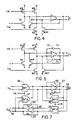
- FIG. 5 A circuit for implementing a DBT damped integrator is shown in Fig. 5.
- An inverting damped integrator is produced by means of a combination of the feedback elements of the devices shown in Figs. 3 and 4.
- the DBT damped integrator of Fig. 5 includes the feedback capacitors 10, 11, each with a capacitance value C f , of Fig. 3 in combina tion with the parallel arranged feedback transistors M1F and M2F of Fig. 4.
- the transfer function of this basic circuit can be shown to be
- any of the three above described inverting building blocks can be changed into a non-inverting equivalent building block by simply interchanging or reversing the two differential output nodes.
- the six basic DBT building blocks thus constitute a family of tunable elements which can be used to implement various monolithic analog filters, as well as other high frequency analog signal processing functions.
- the output waveform of the DBT integrator was again linear over at least a 6V swing.
- the RC time constant of the circuit was adjusted to give varying heights to the triangular output wave.
- the value of the drain voltage VX was adjusted to values of 0.2V, 0.35V, and 0.5 V. The experimental results achieved were very good.
- phase-locked loop PLL
- a source of clock voltage with a fixed frequency (f ext ) is applied to a first input of a phase comparator.
- the output of the phase comparator is applied to the input of a smoothing filter at whose output a common bias voltage (V B ) is developed for all of the tunable RC elements on a semiconductor chip.
- the bias voltage V B is also applied as a control input voltage to control the frequency of an RC oscillator, which can also be realized using a DBT element.
- the output voltage of the oscillator at a frequency f O is applied to a second input of the phase comparator.
- f O is equal to f ext and all of the RC values of the RC elements on the chip are proportional to 1/f ext . Since f ext is precisely controlled, all of the RC values are accurate.
- One drawback of the PLL technique is that it requires the conversion of the output of the phase comparator to a near DC value for V B . This places a high demand on the smoothing filter used in the PLL automatic tuning method.
- a new automatic tuning circuit shown in Fig. 6 provides an alternate method for automatic tuning that avoids the need for phase comparison and filtering, thus making it possible to use a smaller chip area than is possible with the PLL approach.
- the RC time constants of all of the DBT elements on the semiconductor chip are controlled simultaneously by means of an common bias voltage V B .
- the bias voltage generator in Fig. 6 includes first and second integrators, 12 and 13, respectively. Each integrator has one input that is connected to an external clock source via an input terminal 14. The external clock source has a period T ext . Each of the integrators has a second input conncted to a respective current source 15, 16 which supplies a current I k , which need not be precise. The integrators also include capacitors 17, 18 each of a capacitance value C k . The outputs of the integrators are connected via a switching device 19 to the gate electrodes of MOS transistors M1 k and K2 k , which are part of a DBT stage.
- Transistors M1 k and M2 k are connected in series with MOS transistors M3 k and M4 k , respectively, between a source of supply voltage and ground.
- a current source 20 supplies a current I k to the drain of transistor M1 k .
- the drain electrodes of transistors M1 k and M2 k are connected to the non-inverting (+) and inverting (-) inputs, respectively, of an op-amp 21.
- the output of the op-amp provides the bias voltage V B to the various other tunable DBT RC elements 22, 23 etc., which controls the bias currents I B of each of these RC elements.
- the output voltage V B is also coupled to the gate electrodes of transistors M3 k and M4 k to control the bias currents and thereby the drain voltages (VX) of the transistors M1 k and M2 k .
- the two integrators alternately charge and discharge the capacitors to provide continuous operation, thereby avoiding the need for a smoothing filter.
- Each integrator functions to charge up its respective capacitor 17, 18 via its respective current source 15, 16.
- T ext of the external clock source (not shown) coupled to terminal 14 the capacitor 17 or 18 of capacitance C k charges to a potential V k , where
- Fig. 7 shows a second order tunable bandpass/low pass elliptic filter.
- the filter comprises two differential op-amps 24, 25, four DBT elements 26-29, and four capacitors 30-33.
- Each op-amp contains a local feedback circuit that sets the output common mode voltage to V CM .
- the nominal band edge frequency of this filter is set at 20KHz.
- V B By adjusting the bias voltage V B , this frequency can be made to vary from about 10KHz to 40KHz.
- Bandpass and low pass responses are obtained from the outputs 34 (V OBP ) and 35 (V OLP ) respectively.
- V OBP V OBP
- the DBT device in accordance with the invention provides numerous advantages and unique features which will make it possible to generate accurate and controlled RC values in order to implement various high frequency analog signal processing functions, especially, but not limited to, high frequency continuous time analog filters. It will also be appreciated that various modifications and changes in the preferred embodiments disclosed above will occur to those skilled in the art without departing from the spirit and scope of the invention. Therefore, the appended Claims are intended to cover any and all modifications as fall within the spirit of the invention.
Landscapes
- Engineering & Computer Science (AREA)
- Power Engineering (AREA)
- Networks Using Active Elements (AREA)
- Amplifiers (AREA)
- Filters That Use Time-Delay Elements (AREA)
Applications Claiming Priority (2)
| Application Number | Priority Date | Filing Date | Title |
|---|---|---|---|
| US253794 | 1988-10-04 | ||
| US07/253,794 US4918338A (en) | 1988-10-04 | 1988-10-04 | Drain-biassed transresistance device for continuous time filters |
Publications (3)
| Publication Number | Publication Date |
|---|---|
| EP0362935A2 true EP0362935A2 (de) | 1990-04-11 |
| EP0362935A3 EP0362935A3 (en) | 1990-09-12 |
| EP0362935B1 EP0362935B1 (de) | 1995-03-08 |
Family
ID=22961732
Family Applications (1)
| Application Number | Title | Priority Date | Filing Date |
|---|---|---|---|
| EP89202433A Expired - Lifetime EP0362935B1 (de) | 1988-10-04 | 1989-09-28 | Transresistanzvorrichtung mit Drain-Vorspannung |
Country Status (6)
| Country | Link |
|---|---|
| US (1) | US4918338A (de) |
| EP (1) | EP0362935B1 (de) |
| JP (1) | JP3110430B2 (de) |
| KR (1) | KR0130466B1 (de) |
| DE (1) | DE68921532T2 (de) |
| HK (1) | HK76896A (de) |
Cited By (6)
| Publication number | Priority date | Publication date | Assignee | Title |
|---|---|---|---|---|
| EP0802415A1 (de) * | 1996-04-17 | 1997-10-22 | Silicon Systems, Inc. | Stossfühler |
| WO1998036492A1 (en) * | 1997-02-13 | 1998-08-20 | Koninklijke Philips Electronics N.V. | Tuning-range extension circuit for systems utilizing mosfets as tunable resistors |
| EP0818884A3 (de) * | 1996-07-12 | 1998-09-30 | Samsung Electronics Co., Ltd. | Einrichtung zur Stabilisierung der Grenzfrequenz unter Benutzung einer Transkonduktanz |
| WO1998035438A3 (en) * | 1997-02-07 | 1998-11-05 | Koninkl Philips Electronics Nv | Transistorized two-port variable-conductance network |
| US7265609B2 (en) | 2003-05-23 | 2007-09-04 | Koninklijke Philips Electronics N.V. | Transconductor circuits |
| CN101651452B (zh) * | 2009-09-07 | 2012-04-25 | 北京创毅视讯科技有限公司 | 一种rc积分电路 |
Families Citing this family (24)
| Publication number | Priority date | Publication date | Assignee | Title |
|---|---|---|---|---|
| EP0375790A1 (de) * | 1988-10-13 | 1990-07-04 | Siemens Aktiengesellschaft | Integrierbare Filterschaltung |
| US5093628A (en) * | 1990-02-26 | 1992-03-03 | Digital Equipment Corporation Of Canada, Ltd. | Current-pulse integrating circuit and phase-locked loop |
| US5006733A (en) * | 1990-05-11 | 1991-04-09 | Northern Telecom Limited | Filter control circuit |
| CA2100568C (en) * | 1991-01-22 | 2000-11-07 | Sakhawat Khan | Integrated mosfet resistance and oscillator frequency control and trim methods and apparatus |
| US5243239A (en) * | 1991-01-22 | 1993-09-07 | Information Storage Devices, Inc. | Integrated MOSFET resistance and oscillator frequency control and trim methods and apparatus |
| US5097155A (en) * | 1991-02-13 | 1992-03-17 | Industrial Technology Research Institute | Switched-current differentiators and filters |
| US5151662A (en) * | 1991-06-24 | 1992-09-29 | Motorola, Inc. | Circuit and method of signal differentiation |
| US5508570A (en) * | 1993-01-27 | 1996-04-16 | Micro Linear Corporation | Differential amplifier based integrator having a left-half plane pole |
| US5444414A (en) * | 1993-05-28 | 1995-08-22 | National Semiconductor Corporation | Low voltage filter transconductance cell |
| US5608665A (en) * | 1995-10-03 | 1997-03-04 | Wyszynski; Adam S. | Self-tuned, continuous-time active filter |
| JPH10126230A (ja) * | 1996-10-13 | 1998-05-15 | Nippon Steel Corp | 信号入力回路 |
| US5994951A (en) * | 1997-01-21 | 1999-11-30 | Vtc Inc. | Automatic-tuning circuit for integrated continuous-time MOSFET-C filters |
| US6097244A (en) * | 1998-12-17 | 2000-08-01 | Centillium Communications, Inc. | Highly-linear continuous-time filter for a 3-volt supply with PLL-controlled resistor and digitally-controlled capacitor |
| US6987816B1 (en) | 1999-11-23 | 2006-01-17 | Micro Linear Corporation | Iris data recovery algorithms |
| US6441682B1 (en) * | 1999-11-23 | 2002-08-27 | Micro Linear Corporation | Active polyphase filter with transconductor cross-coupling of filter sections |
| US6985541B1 (en) | 1999-11-23 | 2006-01-10 | Micor Linear Corporation | FM demodulator for a low IF receiver |
| US7027792B1 (en) | 1999-11-23 | 2006-04-11 | Micro Linear Corporation | Topology for a single ended input dual balanced mixer |
| US6445257B1 (en) | 1999-11-23 | 2002-09-03 | Micro Linear Corporation | Fuse-trimmed tank circuit for an integrated voltage-controlled oscillator |
| US7076217B1 (en) | 1999-11-23 | 2006-07-11 | Micro Linear Corporation | Integrated radio transceiver |
| US6384637B1 (en) | 2000-06-06 | 2002-05-07 | Rambus | Differential amplifier with selectable hysteresis and buffered filter |
| US9065408B2 (en) * | 2013-03-14 | 2015-06-23 | Rgb Systems, Inc. | Voltage controlled amplifier and method of using the same |
| CN104977450B (zh) * | 2014-04-03 | 2019-04-30 | 深圳市中兴微电子技术有限公司 | 一种电流采样电路及方法 |
| JP2020010088A (ja) * | 2018-07-03 | 2020-01-16 | エイブリック株式会社 | 差動増幅回路 |
| US12603419B2 (en) * | 2021-08-20 | 2026-04-14 | Kymeta Corporation | Driving methods to minimize the effect of leakage current in tunable elements |
Family Cites Families (9)
| Publication number | Priority date | Publication date | Assignee | Title |
|---|---|---|---|---|
| JPS5160432A (de) * | 1974-11-25 | 1976-05-26 | Hitachi Ltd | |
| US3987293A (en) * | 1975-08-04 | 1976-10-19 | Sperry Rand Corporation | Programmable general purpose analog filter |
| US4016481A (en) * | 1975-11-26 | 1977-04-05 | Gte Automatic Electric Laboratories Incorporated | Unmatched field effect transistors providing matched voltage-controlled resistances |
| US4047059A (en) * | 1976-05-24 | 1977-09-06 | Rca Corporation | Comparator circuit |
| US4241316A (en) * | 1979-01-18 | 1980-12-23 | Lawrence Kavanau | Field effect transconductance amplifiers |
| NL8001117A (nl) * | 1980-02-25 | 1981-09-16 | Philips Nv | Versterkertrap met regelbare versterkingsfaktor uitgevoerd met veldeffekttransistoren. |
| US4509019A (en) * | 1983-01-27 | 1985-04-02 | At&T Bell Laboratories | Tunable active filter |
| US4500845A (en) * | 1983-03-15 | 1985-02-19 | Texas Instruments Incorporated | Programmable attenuator |
| US4710726A (en) * | 1986-02-27 | 1987-12-01 | Columbia University In The City Of New York | Semiconductive MOS resistance network |
-
1988
- 1988-10-04 US US07/253,794 patent/US4918338A/en not_active Expired - Lifetime
-
1989
- 1989-09-28 EP EP89202433A patent/EP0362935B1/de not_active Expired - Lifetime
- 1989-09-28 DE DE68921532T patent/DE68921532T2/de not_active Expired - Fee Related
- 1989-09-30 KR KR1019890014080A patent/KR0130466B1/ko not_active Expired - Fee Related
- 1989-10-02 JP JP01257634A patent/JP3110430B2/ja not_active Expired - Fee Related
-
1996
- 1996-05-02 HK HK76896A patent/HK76896A/en not_active IP Right Cessation
Cited By (7)
| Publication number | Priority date | Publication date | Assignee | Title |
|---|---|---|---|---|
| EP0802415A1 (de) * | 1996-04-17 | 1997-10-22 | Silicon Systems, Inc. | Stossfühler |
| EP0818884A3 (de) * | 1996-07-12 | 1998-09-30 | Samsung Electronics Co., Ltd. | Einrichtung zur Stabilisierung der Grenzfrequenz unter Benutzung einer Transkonduktanz |
| CN1076143C (zh) * | 1996-07-12 | 2001-12-12 | 三星电子株式会社 | 利用跨导稳定截止频率的装置 |
| WO1998035438A3 (en) * | 1997-02-07 | 1998-11-05 | Koninkl Philips Electronics Nv | Transistorized two-port variable-conductance network |
| WO1998036492A1 (en) * | 1997-02-13 | 1998-08-20 | Koninklijke Philips Electronics N.V. | Tuning-range extension circuit for systems utilizing mosfets as tunable resistors |
| US7265609B2 (en) | 2003-05-23 | 2007-09-04 | Koninklijke Philips Electronics N.V. | Transconductor circuits |
| CN101651452B (zh) * | 2009-09-07 | 2012-04-25 | 北京创毅视讯科技有限公司 | 一种rc积分电路 |
Also Published As
| Publication number | Publication date |
|---|---|
| KR910007251A (ko) | 1991-04-30 |
| JPH02145009A (ja) | 1990-06-04 |
| DE68921532D1 (de) | 1995-04-13 |
| EP0362935A3 (en) | 1990-09-12 |
| JP3110430B2 (ja) | 2000-11-20 |
| EP0362935B1 (de) | 1995-03-08 |
| DE68921532T2 (de) | 1995-09-21 |
| KR0130466B1 (ko) | 1998-10-01 |
| HK76896A (en) | 1996-05-10 |
| US4918338A (en) | 1990-04-17 |
Similar Documents
| Publication | Publication Date | Title |
|---|---|---|
| EP0362935B1 (de) | Transresistanzvorrichtung mit Drain-Vorspannung | |
| US4823092A (en) | MOS transconductance amplifier for active filters | |
| EP0134221B1 (de) | Regelbarer aktivfilter | |
| Salama et al. | CMOS operational transresistance amplifier for analog signal processing | |
| US6304128B1 (en) | Continuous time capacitor-tuner integrator | |
| Liu et al. | Nonlinear circuit applications with current conveyors | |
| US5227681A (en) | Integration circuit | |
| JPH01129607A (ja) | 精密電圧−デューティサイクル・コンバータ及び低リプル高帯域幅電荷平衡復調器を含む絶縁増幅器 | |
| Veeravalli et al. | A CMOS transconductance amplifier architecture with wide tuning range for very low frequency applications | |
| US6335655B1 (en) | Filter circuit | |
| US4801827A (en) | Adjustable delay element for digital systems | |
| Chen et al. | A systematic realization of third-order quadrature oscillator with controllable amplitude | |
| Kumngern | Realization of electronically tunable first-order allpass filter using single-ended OTAs | |
| Yesil et al. | Electronically controllable bandpass filters with high quality factor and reduced capacitor value: An additional approach | |
| Centurelli et al. | A detailed model of the switched-resistor technique | |
| US7123083B2 (en) | Active filter circuit with operational amplifier | |
| US4763081A (en) | Reducing distortion in active MOSFET-C low pass filters | |
| JPH0542033B2 (de) | ||
| JPS6226606B2 (de) | ||
| JP2002198755A (ja) | 可変利得増幅回路 | |
| Kumngern et al. | Voltage-mode first-order allpass filter using single-ended OTAs and grounded capacitor | |
| Kumngern et al. | A capacitor-grounded current-tunable current mode all-pass network | |
| Mohieldin | High performance continuous-time filters for information transfer systems | |
| Visocchi et al. | The variable gain bootstrap active load: a new approach to amplifier voltage gain enhancement and control | |
| Salmeh | Quality factor tuning of continuous time lowpass filters using a modified LMS algorithm |
Legal Events
| Date | Code | Title | Description |
|---|---|---|---|
| PUAI | Public reference made under article 153(3) epc to a published international application that has entered the european phase |
Free format text: ORIGINAL CODE: 0009012 |
|
| AK | Designated contracting states |
Kind code of ref document: A2 Designated state(s): DE FR GB IT NL |
|
| PUAL | Search report despatched |
Free format text: ORIGINAL CODE: 0009013 |
|
| AK | Designated contracting states |
Kind code of ref document: A3 Designated state(s): DE FR GB IT NL |
|
| 17P | Request for examination filed |
Effective date: 19910308 |
|
| 17Q | First examination report despatched |
Effective date: 19930921 |
|
| GRAA | (expected) grant |
Free format text: ORIGINAL CODE: 0009210 |
|
| AK | Designated contracting states |
Kind code of ref document: B1 Designated state(s): DE FR GB IT NL |
|
| PG25 | Lapsed in a contracting state [announced via postgrant information from national office to epo] |
Ref country code: NL Free format text: LAPSE BECAUSE OF NON-PAYMENT OF DUE FEES Effective date: 19950308 |
|
| REF | Corresponds to: |
Ref document number: 68921532 Country of ref document: DE Date of ref document: 19950413 |
|
| ITF | It: translation for a ep patent filed | ||
| ET | Fr: translation filed | ||
| NLV1 | Nl: lapsed or annulled due to failure to fulfill the requirements of art. 29p and 29m of the patents act | ||
| PLBE | No opposition filed within time limit |
Free format text: ORIGINAL CODE: 0009261 |
|
| STAA | Information on the status of an ep patent application or granted ep patent |
Free format text: STATUS: NO OPPOSITION FILED WITHIN TIME LIMIT |
|
| 26N | No opposition filed | ||
| REG | Reference to a national code |
Ref country code: FR Ref legal event code: CD |
|
| PGFP | Annual fee paid to national office [announced via postgrant information from national office to epo] |
Ref country code: FR Payment date: 20010925 Year of fee payment: 13 |
|
| PGFP | Annual fee paid to national office [announced via postgrant information from national office to epo] |
Ref country code: GB Payment date: 20011001 Year of fee payment: 13 |
|
| PGFP | Annual fee paid to national office [announced via postgrant information from national office to epo] |
Ref country code: DE Payment date: 20011121 Year of fee payment: 13 |
|
| REG | Reference to a national code |
Ref country code: GB Ref legal event code: IF02 |
|
| PG25 | Lapsed in a contracting state [announced via postgrant information from national office to epo] |
Ref country code: GB Free format text: LAPSE BECAUSE OF NON-PAYMENT OF DUE FEES Effective date: 20020928 |
|
| PG25 | Lapsed in a contracting state [announced via postgrant information from national office to epo] |
Ref country code: DE Free format text: LAPSE BECAUSE OF NON-PAYMENT OF DUE FEES Effective date: 20030401 |
|
| GBPC | Gb: european patent ceased through non-payment of renewal fee |
Effective date: 20020928 |
|
| PG25 | Lapsed in a contracting state [announced via postgrant information from national office to epo] |
Ref country code: FR Free format text: LAPSE BECAUSE OF NON-PAYMENT OF DUE FEES Effective date: 20030603 |
|
| REG | Reference to a national code |
Ref country code: FR Ref legal event code: ST |
|
| PG25 | Lapsed in a contracting state [announced via postgrant information from national office to epo] |
Ref country code: IT Free format text: LAPSE BECAUSE OF NON-PAYMENT OF DUE FEES Effective date: 20050928 |