EP0362939A1 - Procédé pour la commande d'un dispositif d'affichage - Google Patents
Procédé pour la commande d'un dispositif d'affichage Download PDFInfo
- Publication number
- EP0362939A1 EP0362939A1 EP89202447A EP89202447A EP0362939A1 EP 0362939 A1 EP0362939 A1 EP 0362939A1 EP 89202447 A EP89202447 A EP 89202447A EP 89202447 A EP89202447 A EP 89202447A EP 0362939 A1 EP0362939 A1 EP 0362939A1
- Authority
- EP
- European Patent Office
- Prior art keywords
- voltage
- pixels
- selection
- switching element
- row
- Prior art date
- Legal status (The legal status is an assumption and is not a legal conclusion. Google has not performed a legal analysis and makes no representation as to the accuracy of the status listed.)
- Granted
Links
- 238000000034 method Methods 0.000 title claims description 23
- 230000005540 biological transmission Effects 0.000 claims description 6
- 238000007599 discharging Methods 0.000 claims description 6
- 239000002184 metal Substances 0.000 claims description 2
- 230000007704 transition Effects 0.000 claims description 2
- 239000004973 liquid crystal related substance Substances 0.000 description 6
- 239000004065 semiconductor Substances 0.000 description 4
- 230000015556 catabolic process Effects 0.000 description 2
- 238000006731 degradation reaction Methods 0.000 description 2
- 230000001419 dependent effect Effects 0.000 description 2
- 230000001627 detrimental effect Effects 0.000 description 1
- 230000008030 elimination Effects 0.000 description 1
- 238000003379 elimination reaction Methods 0.000 description 1
- 150000002500 ions Chemical class 0.000 description 1
- 230000014759 maintenance of location Effects 0.000 description 1
- 238000004519 manufacturing process Methods 0.000 description 1
- 239000000463 material Substances 0.000 description 1
- 239000011159 matrix material Substances 0.000 description 1
- 230000005012 migration Effects 0.000 description 1
- 238000013508 migration Methods 0.000 description 1
- 230000004048 modification Effects 0.000 description 1
- 238000012986 modification Methods 0.000 description 1
Images


Classifications
-
- G—PHYSICS
- G09—EDUCATION; CRYPTOGRAPHY; DISPLAY; ADVERTISING; SEALS
- G09G—ARRANGEMENTS OR CIRCUITS FOR CONTROL OF INDICATING DEVICES USING STATIC MEANS TO PRESENT VARIABLE INFORMATION
- G09G3/00—Control arrangements or circuits, of interest only in connection with visual indicators other than cathode-ray tubes
- G09G3/20—Control arrangements or circuits, of interest only in connection with visual indicators other than cathode-ray tubes for presentation of an assembly of a number of characters, e.g. a page, by composing the assembly by combination of individual elements arranged in a matrix no fixed position being assigned to or needed to be assigned to the individual characters or partial characters
- G09G3/34—Control arrangements or circuits, of interest only in connection with visual indicators other than cathode-ray tubes for presentation of an assembly of a number of characters, e.g. a page, by composing the assembly by combination of individual elements arranged in a matrix no fixed position being assigned to or needed to be assigned to the individual characters or partial characters by control of light from an independent source
- G09G3/36—Control arrangements or circuits, of interest only in connection with visual indicators other than cathode-ray tubes for presentation of an assembly of a number of characters, e.g. a page, by composing the assembly by combination of individual elements arranged in a matrix no fixed position being assigned to or needed to be assigned to the individual characters or partial characters by control of light from an independent source using liquid crystals
- G09G3/3611—Control of matrices with row and column drivers
- G09G3/367—Control of matrices with row and column drivers with a nonlinear element in series with the liquid crystal cell, e.g. a diode, or M.I.M. element
Definitions
- the invention relates to a method of driving a display device comprising an electro-optical display medium between two supporting plates, a system of pixels arranged in rows and columns, with each pixel being at least formed by picture electrodes arranged on the facing surfaces of the supporting plates, at least one picture electrode being connected to a row or column electrode via a non-linear switching element, a row of pixels being selected by means of the switching elements via the row electrodes during at least a part of a line period, while data signals are presented via the column electrodes.
- row electrode and column electrode in this application may be interchanged if desired, so that a column electrode may be meant where reference is made to a row electrode while simultaneously changing column electrode to row electrode.
- an auxiliary voltage across the pixels beyond or on the limit of the voltage range to be used for picture display, for example an auxiliary voltage (reference voltage) or reset voltage.
- a zener diode is arranged between a pixel and a row of column electrode.
- Such a zener diode has a strong asymmetrical current-voltage behaviour (IV-curve).
- a method according to the invention is characterized in that the switching element is at least approximately symmetrical and in that prior to presenting a selection signal, which together with the data signals provides the pixels with a pixel voltage of a certain voltage sign, the pixels are charged or discharged by means of the switching elements to an auxiliary voltage of said same voltage sign, the auxiliary voltage lying beyond or on the limit of the range to be used for picture display.
- the auxiliary voltage is preferably beyond or on the limit of the range of transition in the transmission/voltage characteristic of the electro-optical medium.
- a preferential embodiment of a method according to the invention is characterized in that at least during a number of successive selections, whether preceded by charging or discharging the pixels to an auxiliary voltage or not the current through the symmetrical switching elements has the same direction.
- At least approximately symmetrical switching elements are understood to mean switching elements which have the same or approximately the same current-voltage variation (with opposite sign for current and voltage) such as, for example a MIM (metal-isolator-metal) when reversing the voltage.
- a MIM metal-isolator-metal
- a completely identical variation in both directions is often made substantially impossible by the manufacturing method, in practice the current-voltage curves of such symmetrical switching elements have substantially the same shape in both directions and the on and off voltages in the positive part of the characteristic curve (with the exception of the sign) differ only little from those in the negative part, in contrast to, for example zener diodes.
- symmetrical switching elements are, for example back-to-back diodes and certain semiconductor switching elements such as a nin switching element or a pip switching element (alternately comprising an n (p)-doped semiconductor region, a substantially intrinsic semiconductor region and an n (p)-doped semiconductor region).
- semiconductor switching elements such as a nin switching element or a pip switching element (alternately comprising an n (p)-doped semiconductor region, a substantially intrinsic semiconductor region and an n (p)-doped semiconductor region).
- the symmetrical behaviour can also be obtained by means of a combination of sub-switching elements such as one or more diode rings, a combination of the above-mentioned switching elements, or otherwise.
- the said switching elements may have a considerable spread in, for example the forward voltage so that unwanted voltage components may be introduced resulting in non-uniformities (grey variations) occurring in the display device when conventionally driving the rows with periodical inversion of the polarity of both the selection signals and the non-selection signals (simultaneously with that of the data signals). It is found that these voltage components can be compensated for when used in the method according to the invention in such a way that they hardly influence or do not influence the voltage determining the transmission of the liquid crystal.
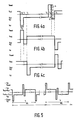
- Fig. 1a shows diagrammatically a device for use of a method according to the invention. Pixels 12 arranged in a matrix are located at the area of crossings of row electrodes 11 and column electrodes 8, while the pixels are connected to the column electrodes 8 via symmetrical non-linear switching elements 15, in this example MIMs.
- Vp1 Vd-Vs1-Vm (1) in which Vm is the forward voltage of the MIM which supplies sufficient current to charge the pixel to the correct voltage within the desired period of time.
- the DC component V DC which may be introduced by the fact that the MIM voltage Vm (or that of another approximately symmetrical switching element) is not identical throughout the surface of the display device and which results in a deviation of the voltage drop across an arbitrary MIM from the nominal value Vm appears to be compensated in practice by a movement of ions in the liquid crystal material so that after some time a direct voltage is only present over the insulating (orientation) layer covering the electrodes.
- the voltage Vampl is independent of the voltage drop across the MIM and possible variations therein. Variations due to nonuniform switching behaviour of the switching elements are therefore not found or are hardly found in the transmission behaviour of the device because possible DC components are compensated for. These DC components are independent of the data voltages (see (4)) so that no image retention or ghost pictures occur.
- a first selection voltage Vs1 is presented on a selection line 11 during a selection period t s while the information or data voltages V d are simultaneously presented on the column electrodes 8; this leads to, for example a positive voltage across a pixel 12 which represents the information presented.
- a negative voltage across the pixel 12 which represents the information presented, is achieved by presenting a second selection voltage Vs2 while simultaneously presenting inverted data voltages (-Vd) after having discharged the capacitance associated with the pixel 12 too far (or after having negatively charged it too far) via the MIM 15.
- Fig. 4 shows how the drive signals are chosen for a plurality of rows of pixels 12 in order to write them with picture information which changes sign during each field (for example in TV applications).
- a selection voltage Vs1 is presented on a row electrode 11 during a selection period ts (which in this example is chosen to be equal to a line period for TV applications, namely 64 ⁇ sec) while information voltages or data voltages Vd are simultaneously presented on the column electrodes 8.
- ts which in this example is chosen to be equal to a line period for TV applications, namely 64 ⁇ sec
- information voltages or data voltages Vd are simultaneously presented on the column electrodes 8.
- Vns1 This voltage is maintained until just before the next selection of the row of pixels 12.
- the reset voltage can then be chosen to be such that the pixels 12 are charged negatively to such an extent via the MIM 15 that the voltage across each associated pixel lies beyond the range to be used for picture display (up to a value of ⁇ -Vsat).
- a subsequent selection period from t4 they are then charged to the desired value determined by data voltages -Vd, via the MIM.
- the row electrodes receive the voltage Vs2 and after the selection period (after t5) has elapsed, they receive a non-selection voltage Vns2. In this way the voltage across the pixels is inverted during each field period.
- Fig. 4b shows the same voltage variation as Fig. 4a but is then shifted over a field period plus a selection period (in this case a line period). This provides the possibility of writing two successive rows of pixels with inverse data voltages with respect to each other.
- Fig. 4c is identical to Fig. 4a, but is shifted over two selection periods.
- the selection voltages Vs1 and Vs2 may of course also be chosen to be shorter than one line period (64 ⁇ sec). In this case the reset voltage may alternatively be presented during a part of the line period in which selection takes place, provided there is sufficient time left to charge the pixels 12.
- the voltage variation on the electrode 11 is then effected, for example in the way as is shown diagrammatically in Fig. 4a by means of the broken line 14.
- the device shown is very suitable for using a drive method in which are chosen for the average voltage across a pixel (see Fig. 2) so that the absolute value of the voltage for the purpose of picture display across the pixels 12 is substantially limited to the range between Vth and Vsat.
- 1/2(Vsat-Vth), i.e. : (1) -1/2(Vsat-Vth) ⁇ Vdmax ⁇ 1/2(VSat-Vth).
- Vs1 -V1-1/2(Vsat+Vth) in which V1 is the forward voltage of the MIM 15.
- Vd-V1-Vs1 the voltage across the pixel 12
- the requirement must be satisfied that the MIMs 15 cannot conduct, or convey such a low current Ioff that discharge via the MIMs 15 is substantially negligible.
- V Amin and V Amax Vns1+Vsat (8)
- V Amin and V Amax V Amax ⁇ -Vdmax+V3 (9) in which -V3 is the voltage at which charging via the MIM is substantially negligible.
- the pixels 12 are subsequently discharged to a value ⁇ -Vsat (see Fig. 4a) by giving the row electrode 11 a sufficiently high reset voltage.
- Vreset ⁇ Vdmax+Vsat+V4 in which -V4 is the voltage of the MIM 15 in the other direction at which sufficient conductance occurs or Vreset ⁇ 1/2(Vsat-Vth)+Vsat+V4 (15)
- V S2 1/2(Vsat+Vth)-V1 is presented on the row electrode 11 while simultaneously presenting data voltages on the column electrodes 8.
- Vns2 Vns2-Vth
- V Amin Vns2-Vsat
- Combination of (16) and (17) leads to: 1/2(Vsat-Vth)-V2+V sat ⁇ Vns2 ⁇ -1/2(Vsat-Vth)+Vth+V3 (18) so that it holds again that: V2+V3 ⁇ 2(Vsat-Vth) (14′)
- the invention is of course not limited to the example described hereinbefore, but it may alternatively be used in devices comprising different non-linear approximately symmetrical switching elements such as a back-to-back diode, a nin or a pip switching element.
- the switching element and the display element may also exchange positions as is shown diagrammmatically in Fig. 1b.
- a non-linear approximately symmetrical switching element may alternatively be assembled from different sub-switching elements as in the case of one or more diode rings or when providing redundancy, in a manner similar to that described in Netherlands Patent Application no. 8,800,204 (PHN 12.409).
- the row electrodes need not be connected directly to the picture electrodes but they may be capacitively coupled thereto, as has been described in greater detail in the non-prepublished Netherlands Patent Application no. 8,802,155 (PHN 12.651) in the name of the Applicant.
- An extra (storage) capacitance may be arranged parallel to the pixel between the column electrode and the row electrode.
- a second reset voltage can be presented to the row electrode 11 which in a manner known per se charges the pixels tyo an auxiliary voltage of a sign opposite to the voltage sign obtained during the selecting period following immediately thereafter.
- a second reset voltage can be presented to the row electrode 11 which in a manner known per se charges the pixels tyo an auxiliary voltage of a sign opposite to the voltage sign obtained during the selecting period following immediately thereafter.
Landscapes
- Engineering & Computer Science (AREA)
- Chemical & Material Sciences (AREA)
- Crystallography & Structural Chemistry (AREA)
- Physics & Mathematics (AREA)
- Computer Hardware Design (AREA)
- General Physics & Mathematics (AREA)
- Theoretical Computer Science (AREA)
- Liquid Crystal (AREA)
- Liquid Crystal Display Device Control (AREA)
- Control Of Indicators Other Than Cathode Ray Tubes (AREA)
- Selective Calling Equipment (AREA)
- Electrochromic Elements, Electrophoresis, Or Variable Reflection Or Absorption Elements (AREA)
Applications Claiming Priority (2)
| Application Number | Priority Date | Filing Date | Title |
|---|---|---|---|
| NL8802436A NL8802436A (nl) | 1988-10-05 | 1988-10-05 | Werkwijze voor het besturen van een weergeefinrichting. |
| NL8802436 | 1988-10-05 |
Publications (2)
| Publication Number | Publication Date |
|---|---|
| EP0362939A1 true EP0362939A1 (fr) | 1990-04-11 |
| EP0362939B1 EP0362939B1 (fr) | 1994-12-14 |
Family
ID=19852996
Family Applications (1)
| Application Number | Title | Priority Date | Filing Date |
|---|---|---|---|
| EP89202447A Expired - Lifetime EP0362939B1 (fr) | 1988-10-05 | 1989-09-29 | Procédé pour la commande d'un dispositif d'affichage |
Country Status (9)
| Country | Link |
|---|---|
| US (1) | US5159325A (fr) |
| EP (1) | EP0362939B1 (fr) |
| JP (1) | JP2582302B2 (fr) |
| KR (1) | KR970006861B1 (fr) |
| CN (1) | CN1018301B (fr) |
| AT (1) | ATE115757T1 (fr) |
| DE (1) | DE68919980T2 (fr) |
| HK (1) | HK164796A (fr) |
| NL (1) | NL8802436A (fr) |
Cited By (6)
| Publication number | Priority date | Publication date | Assignee | Title |
|---|---|---|---|---|
| EP0479291A3 (en) * | 1990-10-05 | 1992-09-30 | Kabushiki Kaisha Toshiba | Method and apparatus for driving liquid crystal display device |
| EP0448032A3 (en) * | 1990-03-20 | 1992-11-19 | Canon Kabushiki Kaisha | Method of driving ferroelectric liquid crystal element |
| US5227900A (en) * | 1990-03-20 | 1993-07-13 | Canon Kabushiki Kaisha | Method of driving ferroelectric liquid crystal element |
| US5428370A (en) * | 1991-07-17 | 1995-06-27 | U.S. Philips Corporation | Matrix display device and its method of operation |
| US5892504A (en) * | 1991-07-17 | 1999-04-06 | U.S. Philips Corporation | Matrix display device and its method of operation |
| EP1033902A3 (fr) * | 1999-03-04 | 2004-08-18 | Pioneer Corporation | Dispositif d'affichage à base des sources lumineuses capacitives |
Families Citing this family (23)
| Publication number | Priority date | Publication date | Assignee | Title |
|---|---|---|---|---|
| US5790089A (en) * | 1991-03-20 | 1998-08-04 | Seiko Epson Corporation | Method of driving an active matrix type liquid crystal display |
| TW200572B (fr) * | 1991-03-20 | 1993-02-21 | Seiko Epson Corp | |
| US6271817B1 (en) | 1991-03-20 | 2001-08-07 | Seiko Epson Corporation | Method of driving liquid crystal display device that reduces afterimages |
| JP2831518B2 (ja) * | 1992-10-30 | 1998-12-02 | シャープ株式会社 | 表示装置の駆動回路 |
| US5426447A (en) * | 1992-11-04 | 1995-06-20 | Yuen Foong Yu H.K. Co., Ltd. | Data driving circuit for LCD display |
| US5313222A (en) * | 1992-12-24 | 1994-05-17 | Yuen Foong Yu H. K. Co., Ltd. | Select driver circuit for an LCD display |
| US5510807A (en) * | 1993-01-05 | 1996-04-23 | Yuen Foong Yu H.K. Co., Ltd. | Data driver circuit and associated method for use with scanned LCD video display |
| GB9305608D0 (en) * | 1993-03-18 | 1993-05-05 | Philips Electronics Uk Ltd | Method of driving a matrix display device |
| EP0699332B1 (fr) * | 1994-03-18 | 2000-01-12 | Koninklijke Philips Electronics N.V. | Dispositif d'affichage a matrice active et son procede de commande |
| KR960702657A (ko) * | 1994-03-23 | 1996-04-27 | 프레데릭 얀 스미트 | 디스플레이 장치(Display device) |
| TW409928U (en) * | 1994-03-31 | 2000-10-21 | Flat Panel Display Co Fpd Bv | Display device |
| US5767829A (en) * | 1994-08-23 | 1998-06-16 | U.S. Philips Corporation | Liquid crystal display device including drive circuit for predetermining polarization state |
| US5644357A (en) * | 1994-12-15 | 1997-07-01 | Philips Electronics North America Corporation | Burst driving of single-panel display |
| US5805122A (en) * | 1994-12-16 | 1998-09-08 | Philips Electronics North America Corporation | Voltage driving waveforms for plasma addressed liquid crystal displays |
| WO1996021881A1 (fr) * | 1995-01-13 | 1996-07-18 | Flat Panel Display Co. (Fpd) B.V. | Dispositif d'affichage a cristaux liquides |
| JPH10509533A (ja) * | 1995-09-11 | 1998-09-14 | フラット パネル ディスプレイ カンパニー ベスローテン フェンノートシャップ エフペーデー | 液晶表示装置 |
| GB9524071D0 (en) * | 1995-11-24 | 1996-01-24 | Philips Electronics Nv | Active matrix diplay device |
| WO1997031362A1 (fr) * | 1996-02-22 | 1997-08-28 | Philips Electronics N.V. | Dispositif d'affichage a cristaux liquides |
| GB9704149D0 (en) | 1996-08-16 | 1997-04-16 | Philips Electronics Nv | Active matrix display devices and methods of driving such |
| JP3617206B2 (ja) * | 1996-08-16 | 2005-02-02 | セイコーエプソン株式会社 | 表示装置、電子機器及び駆動方法 |
| US7411573B2 (en) * | 2001-06-08 | 2008-08-12 | Thomson Licensing | LCOS column memory effect reduction |
| US7190008B2 (en) * | 2002-04-24 | 2007-03-13 | E Ink Corporation | Electro-optic displays, and components for use therein |
| KR101026802B1 (ko) * | 2003-11-18 | 2011-04-04 | 삼성전자주식회사 | 액정 표시 장치 및 그 구동 방법 |
Citations (7)
| Publication number | Priority date | Publication date | Assignee | Title |
|---|---|---|---|---|
| US4223308A (en) * | 1979-07-25 | 1980-09-16 | Northern Telecom Limited | LCDs (Liquid crystal displays) controlled by thin film diode switches |
| US4251136A (en) * | 1979-07-25 | 1981-02-17 | Northern Telecom Limited | LCDs (Liquid crystal displays) controlled by thin film diode switches |
| US4413883A (en) * | 1979-05-31 | 1983-11-08 | Northern Telecom Limited | Displays controlled by MIM switches of small capacitance |
| FR2533730A1 (fr) * | 1982-09-27 | 1984-03-30 | Citizen Watch Co Ltd | Procede de commande d'un dispositif d'affichage a matrice |
| FR2549265A1 (fr) * | 1983-07-13 | 1985-01-18 | Citizen Watch Co Ltd | Panneau de visualisation de type matrice |
| EP0217469A1 (fr) * | 1985-09-30 | 1987-04-08 | Koninklijke Philips Electronics N.V. | Dispositif d'affichage à commande d'attaque |
| US4667189A (en) * | 1984-04-25 | 1987-05-19 | Energy Conversion Devices, Inc. | Programmable semiconductor switch for a display matrix or the like and method for making same |
Family Cites Families (11)
| Publication number | Priority date | Publication date | Assignee | Title |
|---|---|---|---|---|
| US3654606A (en) * | 1969-11-06 | 1972-04-04 | Rca Corp | Alternating voltage excitation of liquid crystal display matrix |
| DE3019832C2 (de) * | 1979-05-28 | 1986-10-16 | Kabushiki Kaisha Suwa Seikosha, Shinjuku, Tokio/Tokyo | Treiberschaltung für eine Flüssigkristallanzeigematrix |
| NL8103376A (nl) * | 1981-07-16 | 1983-02-16 | Philips Nv | Weergeefinrichting. |
| JPS60203920A (ja) * | 1984-03-28 | 1985-10-15 | Canon Inc | 液晶光学素子の駆動法 |
| JP2572578B2 (ja) * | 1985-09-26 | 1997-01-16 | セイコーエプソン株式会社 | 画像表示装置及びその駆動方法 |
| JPS62150334A (ja) * | 1985-12-25 | 1987-07-04 | Canon Inc | 液晶装置 |
| NL8601373A (nl) * | 1986-05-29 | 1987-12-16 | Philips Nv | Weergeefinrichting met verbeterde aansturing. |
| JPS63198097A (ja) * | 1987-02-13 | 1988-08-16 | セイコーインスツルメンツ株式会社 | 非線形2端子型アクテイブマトリクス表示装置 |
| EP0288011A3 (fr) * | 1987-04-20 | 1991-02-20 | Hitachi, Ltd. | Dispositif d'affichage à cristaux liquides et méthode de commande pour ce dispositif |
| NL8701420A (nl) * | 1987-06-18 | 1989-01-16 | Philips Nv | Weergeefinrichting en werkwijze voor het besturen van een dergelijke weergeefinrichting. |
| EP0296662B1 (fr) * | 1987-06-18 | 1992-06-03 | Koninklijke Philips Electronics N.V. | Dispositif d'affichage et méthode de commande d'un tel dispositif |
-
1988
- 1988-10-05 NL NL8802436A patent/NL8802436A/nl not_active Application Discontinuation
-
1989
- 1989-09-28 JP JP1253700A patent/JP2582302B2/ja not_active Expired - Fee Related
- 1989-09-29 KR KR89014009A patent/KR970006861B1/ko not_active Expired - Fee Related
- 1989-09-29 EP EP89202447A patent/EP0362939B1/fr not_active Expired - Lifetime
- 1989-09-29 AT AT89202447T patent/ATE115757T1/de not_active IP Right Cessation
- 1989-09-29 US US07/414,565 patent/US5159325A/en not_active Expired - Fee Related
- 1989-09-29 DE DE68919980T patent/DE68919980T2/de not_active Expired - Fee Related
- 1989-10-02 CN CN89107722A patent/CN1018301B/zh not_active Expired
-
1996
- 1996-09-05 HK HK164796A patent/HK164796A/en not_active IP Right Cessation
Patent Citations (8)
| Publication number | Priority date | Publication date | Assignee | Title |
|---|---|---|---|---|
| US4413883A (en) * | 1979-05-31 | 1983-11-08 | Northern Telecom Limited | Displays controlled by MIM switches of small capacitance |
| US4413883B1 (fr) * | 1979-05-31 | 1991-06-04 | Northern Telecom Ltd | |
| US4223308A (en) * | 1979-07-25 | 1980-09-16 | Northern Telecom Limited | LCDs (Liquid crystal displays) controlled by thin film diode switches |
| US4251136A (en) * | 1979-07-25 | 1981-02-17 | Northern Telecom Limited | LCDs (Liquid crystal displays) controlled by thin film diode switches |
| FR2533730A1 (fr) * | 1982-09-27 | 1984-03-30 | Citizen Watch Co Ltd | Procede de commande d'un dispositif d'affichage a matrice |
| FR2549265A1 (fr) * | 1983-07-13 | 1985-01-18 | Citizen Watch Co Ltd | Panneau de visualisation de type matrice |
| US4667189A (en) * | 1984-04-25 | 1987-05-19 | Energy Conversion Devices, Inc. | Programmable semiconductor switch for a display matrix or the like and method for making same |
| EP0217469A1 (fr) * | 1985-09-30 | 1987-04-08 | Koninklijke Philips Electronics N.V. | Dispositif d'affichage à commande d'attaque |
Cited By (6)
| Publication number | Priority date | Publication date | Assignee | Title |
|---|---|---|---|---|
| EP0448032A3 (en) * | 1990-03-20 | 1992-11-19 | Canon Kabushiki Kaisha | Method of driving ferroelectric liquid crystal element |
| US5227900A (en) * | 1990-03-20 | 1993-07-13 | Canon Kabushiki Kaisha | Method of driving ferroelectric liquid crystal element |
| EP0479291A3 (en) * | 1990-10-05 | 1992-09-30 | Kabushiki Kaisha Toshiba | Method and apparatus for driving liquid crystal display device |
| US5428370A (en) * | 1991-07-17 | 1995-06-27 | U.S. Philips Corporation | Matrix display device and its method of operation |
| US5892504A (en) * | 1991-07-17 | 1999-04-06 | U.S. Philips Corporation | Matrix display device and its method of operation |
| EP1033902A3 (fr) * | 1999-03-04 | 2004-08-18 | Pioneer Corporation | Dispositif d'affichage à base des sources lumineuses capacitives |
Also Published As
| Publication number | Publication date |
|---|---|
| DE68919980T2 (de) | 1995-06-29 |
| CN1041840A (zh) | 1990-05-02 |
| KR970006861B1 (ko) | 1997-04-30 |
| US5159325A (en) | 1992-10-27 |
| JP2582302B2 (ja) | 1997-02-19 |
| EP0362939B1 (fr) | 1994-12-14 |
| JPH02125225A (ja) | 1990-05-14 |
| KR910006911A (ko) | 1991-04-30 |
| CN1018301B (zh) | 1992-09-16 |
| DE68919980D1 (de) | 1995-01-26 |
| ATE115757T1 (de) | 1994-12-15 |
| NL8802436A (nl) | 1990-05-01 |
| HK164796A (en) | 1996-09-12 |
Similar Documents
| Publication | Publication Date | Title |
|---|---|---|
| US5159325A (en) | Method of driving a display device | |
| EP0299546B1 (fr) | Dispositif d'affichage et méthode de commande d'un tel dispositif | |
| US5648794A (en) | Display device | |
| JP4567710B2 (ja) | ディスプレイ装置及びその行選択ラインスキャナ | |
| US5898416A (en) | Display device | |
| US4811006A (en) | Display arrangement with improved drive | |
| EP0489459B1 (fr) | Méthode de commande d'un dispositif d'affichage matriciel et un dispositif d'affichage matriciel commandé par cette méthode | |
| EP0269150B1 (fr) | Méthode de commande d'un dispositif d'affichage et dispositif d'affichage convenant à une telle méthode | |
| EP0296663A1 (fr) | Dispositif d'affichage | |
| US4810059A (en) | Display device with three-level drive | |
| US5032830A (en) | Electro-optical display device with non-linear switching units with auxiliary voltages and capacitively coupled row electrodes | |
| EP0296662B1 (fr) | Dispositif d'affichage et méthode de commande d'un tel dispositif | |
| EP0420340B1 (fr) | Dispositif de reproduction | |
| JP3243583B2 (ja) | アクティブマトリクス型液晶表示装置 | |
| WO1996016392A1 (fr) | Circuit de correction destine a compenser des changements de parametres dans un affichage a matrice active |
Legal Events
| Date | Code | Title | Description |
|---|---|---|---|
| PUAI | Public reference made under article 153(3) epc to a published international application that has entered the european phase |
Free format text: ORIGINAL CODE: 0009012 |
|
| AK | Designated contracting states |
Kind code of ref document: A1 Designated state(s): AT CH DE ES FR GB IT LI NL SE |
|
| 17P | Request for examination filed |
Effective date: 19901009 |
|
| 17Q | First examination report despatched |
Effective date: 19920727 |
|
| GRAA | (expected) grant |
Free format text: ORIGINAL CODE: 0009210 |
|
| AK | Designated contracting states |
Kind code of ref document: B1 Designated state(s): AT CH DE ES FR GB IT LI NL SE |
|
| PG25 | Lapsed in a contracting state [announced via postgrant information from national office to epo] |
Ref country code: NL Effective date: 19941214 Ref country code: LI Effective date: 19941214 Ref country code: ES Free format text: THE PATENT HAS BEEN ANNULLED BY A DECISION OF A NATIONAL AUTHORITY Effective date: 19941214 Ref country code: CH Effective date: 19941214 Ref country code: AT Effective date: 19941214 |
|
| REF | Corresponds to: |
Ref document number: 115757 Country of ref document: AT Date of ref document: 19941215 Kind code of ref document: T |
|
| REF | Corresponds to: |
Ref document number: 68919980 Country of ref document: DE Date of ref document: 19950126 |
|
| ITF | It: translation for a ep patent filed | ||
| PG25 | Lapsed in a contracting state [announced via postgrant information from national office to epo] |
Ref country code: SE Effective date: 19950314 |
|
| ET | Fr: translation filed | ||
| REG | Reference to a national code |
Ref country code: CH Ref legal event code: PL |
|
| ITPR | It: changes in ownership of a european patent |
Owner name: CAMBIO RAGIONE SOCIALE;PHILIPS ELECTRONICS N.V. |
|
| NLV1 | Nl: lapsed or annulled due to failure to fulfill the requirements of art. 29p and 29m of the patents act | ||
| REG | Reference to a national code |
Ref country code: FR Ref legal event code: CD |
|
| PGFP | Annual fee paid to national office [announced via postgrant information from national office to epo] |
Ref country code: GR Payment date: 19950728 Year of fee payment: 7 |
|
| PLBE | No opposition filed within time limit |
Free format text: ORIGINAL CODE: 0009261 |
|
| STAA | Information on the status of an ep patent application or granted ep patent |
Free format text: STATUS: NO OPPOSITION FILED WITHIN TIME LIMIT |
|
| 26N | No opposition filed | ||
| REG | Reference to a national code |
Ref country code: FR Ref legal event code: CD |
|
| REG | Reference to a national code |
Ref country code: GB Ref legal event code: IF02 |
|
| PGFP | Annual fee paid to national office [announced via postgrant information from national office to epo] |
Ref country code: FR Payment date: 20030926 Year of fee payment: 15 |
|
| PGFP | Annual fee paid to national office [announced via postgrant information from national office to epo] |
Ref country code: GB Payment date: 20030930 Year of fee payment: 15 |
|
| PGFP | Annual fee paid to national office [announced via postgrant information from national office to epo] |
Ref country code: DE Payment date: 20031126 Year of fee payment: 15 |
|
| PG25 | Lapsed in a contracting state [announced via postgrant information from national office to epo] |
Ref country code: GB Free format text: LAPSE BECAUSE OF NON-PAYMENT OF DUE FEES Effective date: 20040929 |
|
| PG25 | Lapsed in a contracting state [announced via postgrant information from national office to epo] |
Ref country code: DE Free format text: LAPSE BECAUSE OF NON-PAYMENT OF DUE FEES Effective date: 20050401 |
|
| GBPC | Gb: european patent ceased through non-payment of renewal fee |
Effective date: 20040929 |
|
| PG25 | Lapsed in a contracting state [announced via postgrant information from national office to epo] |
Ref country code: FR Free format text: LAPSE BECAUSE OF NON-PAYMENT OF DUE FEES Effective date: 20050531 |
|
| REG | Reference to a national code |
Ref country code: FR Ref legal event code: ST |
|
| PG25 | Lapsed in a contracting state [announced via postgrant information from national office to epo] |
Ref country code: IT Free format text: LAPSE BECAUSE OF NON-PAYMENT OF DUE FEES;WARNING: LAPSES OF ITALIAN PATENTS WITH EFFECTIVE DATE BEFORE 2007 MAY HAVE OCCURRED AT ANY TIME BEFORE 2007. THE CORRECT EFFECTIVE DATE MAY BE DIFFERENT FROM THE ONE RECORDED. Effective date: 20050929 |