EP0362961A1 - Verfahren zum Betrieb einer MOS-Struktur und MOS-Struktur dafür - Google Patents
Verfahren zum Betrieb einer MOS-Struktur und MOS-Struktur dafür Download PDFInfo
- Publication number
- EP0362961A1 EP0362961A1 EP89202497A EP89202497A EP0362961A1 EP 0362961 A1 EP0362961 A1 EP 0362961A1 EP 89202497 A EP89202497 A EP 89202497A EP 89202497 A EP89202497 A EP 89202497A EP 0362961 A1 EP0362961 A1 EP 0362961A1
- Authority
- EP
- European Patent Office
- Prior art keywords
- back gate
- volt
- voltage
- mos
- soi
- Prior art date
- Legal status (The legal status is an assumption and is not a legal conclusion. Google has not performed a legal analysis and makes no representation as to the accuracy of the status listed.)
- Granted
Links
Images


Classifications
-
- H—ELECTRICITY
- H10—SEMICONDUCTOR DEVICES; ELECTRIC SOLID-STATE DEVICES NOT OTHERWISE PROVIDED FOR
- H10D—INORGANIC ELECTRIC SEMICONDUCTOR DEVICES
- H10D48/00—Individual devices not covered by groups H10D1/00 - H10D44/00
- H10D48/387—Devices controllable only by the variation of applied heat
-
- H—ELECTRICITY
- H10—SEMICONDUCTOR DEVICES; ELECTRIC SOLID-STATE DEVICES NOT OTHERWISE PROVIDED FOR
- H10D—INORGANIC ELECTRIC SEMICONDUCTOR DEVICES
- H10D86/00—Integrated devices formed in or on insulating or conducting substrates, e.g. formed in silicon-on-insulator [SOI] substrates or on stainless steel or glass substrates
- H10D86/201—Integrated devices formed in or on insulating or conducting substrates, e.g. formed in silicon-on-insulator [SOI] substrates or on stainless steel or glass substrates the substrates comprising an insulating layer on a semiconductor body, e.g. SOI
Definitions
- the present invention relates to the field of MOS-structures, more particular to a SOI-nMOS (Silicon-on-Insulator-n type-Metal-Oxide-Semiconductor) structure.
- SOI-nMOS Silicon-on-Insulator-n type-Metal-Oxide-Semiconductor
- the present invention provides a method of operating a SOI-structure provided with a back gate, comprising the following steps: - cooling the SOI-structure; and - supplying and/or draining electrical charge in a cavity of the SOI-structure at predetermined times.
- bistable condition of such a transistor can be obtained.
- This bistable condition or behaviour can be advantageously used as an elegantly simple memory element.
- the present invention provides a semiconductor structure.
- a SOI-structure 1 (fig. 1 and 2) comprises a backgate 2, an insulating layer 3 and a N+ silicon film 4 provided thereto in which a so-called SOI cavity is included, in which a P ⁇ region 5 is provided.
- a front insulating layer 6 is provided to the Si-layer 4 and the P ⁇ region 5, to which layer 6 the front gate 7 is provided.
- the backgate 2 comprises silicon
- the layer 3 is formed of SiO2 by means of oxydation and the film 4 is formed by deposition, after which the film is crystallized preferably by a laser.
- such a cavity charge condition is maintained during a certain time period, as such structure is being cooled. Therefore a multistable or bistable condition of the semiconductor structure is obtained, by means of which e.g. a memory effect is to be obtained.
- the threshold voltage V T of the P-region 5 is adjustable such that the current characteristic of this region is controlable.
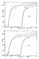
- Fig. 3 shows a graph of the drain current I d as function of the voltage to the front gate V gf , in which the SOI-NMOS-structure was held at 77 K.
- Curves A and C represent the situation in which a voltage of 3.5 Volt was supplied to the P ⁇ region 5, while in the situation of curves B and D a voltage of V D is 0.5 Volt was applied.
- the back gate 2 was pulsed starting from a DC-voltage of -20 Volt to 0, - 40 Volt resp. and vice versa, in which the difference between curves A and B on the one hand and curves C and D on the other hand was obtained.
- Curves A and B provide a threshold voltage V T of 1.2 Volt
- curves C and D provide a threshold voltage V T of 3 Volt.
- the graph of fig. 5 was obtained by cooling the structure to 4 K. Further, the circumstances for the curves E and F are similar to those for curves A and B and those of curves G and H to those for curves C and D, viz. pulses from -20 Volt to -40 Volt from -20 Volt to 0 Volt, resp.
- the pulses bias the junctions between N+- and P ⁇ region forwardly temporarily, whereby the amount of charge stored in the P ⁇ region (cavity) is influenced.
- the semiconductor element 1 according to the present invention is compact and may be driven at high rate.
- Fig. 6 shows a circuit diagram in which two transistors T1 and T2 are added to the semiconductor 1, which circuit is suited for RAM-like applications.
- terminals A, B and C By including terminals A, B and C in a matrix read/write/refresh-signals will be obtained.
- the desired voltages at terminals A, B and C are dependant on the W/L ratio of the semiconductor structure, as well as those of transistors T1 and T2.
- a typical embodiment of a SOI-NMOS-transistor com simplyprises e.g. an Si-layer 4 of 500 nm, a back oxide of e.g. 500 nm and a borium concentration of 1016 cm ⁇ 3.
- the threshold voltage V T can be influenced in this embodiments through the cavity charge Q cav , as well as through the front gate voltage V gb , which influence can be correlated. Bias voltages and pulse width(s) are dependant on the chosen thickness of the layers.
- a transistor according to the present invention is hardened to radiation influence.
- Each semiconductor element can be controlled (refreshed) through a separate back gate in future three dimensional integrated circuits.
Landscapes
- Thin Film Transistor (AREA)
- Semiconductor Memories (AREA)
- Metal-Oxide And Bipolar Metal-Oxide Semiconductor Integrated Circuits (AREA)
- Analysing Materials By The Use Of Radiation (AREA)
- Solid State Image Pick-Up Elements (AREA)
Priority Applications (1)
| Application Number | Priority Date | Filing Date | Title |
|---|---|---|---|
| AT89202497T ATE101753T1 (de) | 1988-10-03 | 1989-10-03 | Verfahren zum betrieb einer mos-struktur und mos- struktur dafuer. |
Applications Claiming Priority (2)
| Application Number | Priority Date | Filing Date | Title |
|---|---|---|---|
| NL8802423A NL8802423A (nl) | 1988-10-03 | 1988-10-03 | Werkwijze voor het bedrijven van een mos-structuur en daarvoor geschikte mos-structuur. |
| NL8802423 | 1988-10-03 |
Publications (2)
| Publication Number | Publication Date |
|---|---|
| EP0362961A1 true EP0362961A1 (de) | 1990-04-11 |
| EP0362961B1 EP0362961B1 (de) | 1994-02-16 |
Family
ID=19852988
Family Applications (1)
| Application Number | Title | Priority Date | Filing Date |
|---|---|---|---|
| EP89202497A Expired - Lifetime EP0362961B1 (de) | 1988-10-03 | 1989-10-03 | Verfahren zum Betrieb einer MOS-Struktur und MOS-Struktur dafür |
Country Status (7)
| Country | Link |
|---|---|
| EP (1) | EP0362961B1 (de) |
| JP (1) | JPH02150066A (de) |
| AT (1) | ATE101753T1 (de) |
| CA (1) | CA1323942C (de) |
| DE (1) | DE68913119T2 (de) |
| ES (1) | ES2049317T3 (de) |
| NL (1) | NL8802423A (de) |
Cited By (21)
| Publication number | Priority date | Publication date | Assignee | Title |
|---|---|---|---|---|
| US6873539B1 (en) | 2001-06-18 | 2005-03-29 | Pierre Fazan | Semiconductor device |
| WO2013026237A1 (zh) * | 2011-08-22 | 2013-02-28 | 中国科学院微电子研究所 | 半导体器件 |
| US8861247B2 (en) | 2009-04-27 | 2014-10-14 | Micron Technology, Inc. | Techniques for providing a direct injection semiconductor memory device |
| US8947965B2 (en) | 2009-07-27 | 2015-02-03 | Micron Technology Inc. | Techniques for providing a direct injection semiconductor memory device |
| US8964479B2 (en) | 2010-03-04 | 2015-02-24 | Micron Technology, Inc. | Techniques for sensing a semiconductor memory device |
| US8982633B2 (en) | 2009-05-22 | 2015-03-17 | Micron Technology, Inc. | Techniques for providing a direct injection semiconductor memory device |
| US9012963B2 (en) | 2011-08-22 | 2015-04-21 | Institute of Microelectronics, Chinese Academy of Sciences | Semiconductor device |
| US9019759B2 (en) | 2010-03-15 | 2015-04-28 | Micron Technology, Inc. | Techniques for providing a semiconductor memory device |
| US9019788B2 (en) | 2008-01-24 | 2015-04-28 | Micron Technology, Inc. | Techniques for accessing memory cells |
| US9064730B2 (en) | 2009-03-04 | 2015-06-23 | Micron Technology, Inc. | Techniques for forming a contact to a buried diffusion layer in a semiconductor memory device |
| US9093311B2 (en) | 2009-03-31 | 2015-07-28 | Micron Technology, Inc. | Techniques for providing a semiconductor memory device |
| US9142264B2 (en) | 2010-05-06 | 2015-09-22 | Micron Technology, Inc. | Techniques for refreshing a semiconductor memory device |
| US9240496B2 (en) | 2009-04-30 | 2016-01-19 | Micron Technology, Inc. | Semiconductor device with floating gate and electrically floating body |
| US9257155B2 (en) | 2007-05-30 | 2016-02-09 | Micron Technology, Inc. | Integrated circuit having voltage generation circuitry for memory cell array, and method of operating and/or controlling same |
| US9263133B2 (en) | 2011-05-17 | 2016-02-16 | Micron Technology, Inc. | Techniques for providing a semiconductor memory device |
| US9276000B2 (en) | 2007-03-29 | 2016-03-01 | Micron Technology, Inc. | Manufacturing process for zero-capacitor random access memory circuits |
| US9331083B2 (en) | 2009-07-10 | 2016-05-03 | Micron Technology, Inc. | Techniques for providing a semiconductor memory device |
| US9553186B2 (en) | 2008-09-25 | 2017-01-24 | Micron Technology, Inc. | Recessed gate silicon-on-insulator floating body device with self-aligned lateral isolation |
| US9812179B2 (en) | 2009-11-24 | 2017-11-07 | Ovonyx Memory Technology, Llc | Techniques for reducing disturbance in a semiconductor memory device |
| US10304837B2 (en) | 2007-11-29 | 2019-05-28 | Ovonyx Memory Technology, Llc | Integrated circuit having memory cell array including barriers, and method of manufacturing same |
| US10418091B2 (en) | 2005-09-07 | 2019-09-17 | Ovonyx Memory Technology, Llc | Memory cell and memory cell array having an electrically floating body transistor, and methods of operating same |
Families Citing this family (37)
| Publication number | Priority date | Publication date | Assignee | Title |
|---|---|---|---|---|
| EP1357603A3 (de) | 2002-04-18 | 2004-01-14 | Innovative Silicon SA | Halbleiterbauelement |
| EP1355316B1 (de) | 2002-04-18 | 2007-02-21 | Innovative Silicon SA | Datenspeichergerät sowie Verfahren zum Auffrischen der auf einem solchen Gerät gespeicherten Daten |
| US6912150B2 (en) | 2003-05-13 | 2005-06-28 | Lionel Portman | Reference current generator, and method of programming, adjusting and/or operating same |
| US7085153B2 (en) | 2003-05-13 | 2006-08-01 | Innovative Silicon S.A. | Semiconductor memory cell, array, architecture and device, and method of operating same |
| US20040228168A1 (en) | 2003-05-13 | 2004-11-18 | Richard Ferrant | Semiconductor memory device and method of operating same |
| US7335934B2 (en) | 2003-07-22 | 2008-02-26 | Innovative Silicon S.A. | Integrated circuit device, and method of fabricating same |
| US7184298B2 (en) | 2003-09-24 | 2007-02-27 | Innovative Silicon S.A. | Low power programming technique for a floating body memory transistor, memory cell, and memory array |
| US7476939B2 (en) | 2004-11-04 | 2009-01-13 | Innovative Silicon Isi Sa | Memory cell having an electrically floating body transistor and programming technique therefor |
| US7251164B2 (en) | 2004-11-10 | 2007-07-31 | Innovative Silicon S.A. | Circuitry for and method of improving statistical distribution of integrated circuits |
| US7301838B2 (en) | 2004-12-13 | 2007-11-27 | Innovative Silicon S.A. | Sense amplifier circuitry and architecture to write data into and/or read from memory cells |
| US7301803B2 (en) | 2004-12-22 | 2007-11-27 | Innovative Silicon S.A. | Bipolar reading technique for a memory cell having an electrically floating body transistor |
| US7355916B2 (en) | 2005-09-19 | 2008-04-08 | Innovative Silicon S.A. | Method and circuitry to generate a reference current for reading a memory cell, and device implementing same |
| US7683430B2 (en) | 2005-12-19 | 2010-03-23 | Innovative Silicon Isi Sa | Electrically floating body memory cell and array, and method of operating or controlling same |
| US7542345B2 (en) | 2006-02-16 | 2009-06-02 | Innovative Silicon Isi Sa | Multi-bit memory cell having electrically floating body transistor, and method of programming and reading same |
| US7492632B2 (en) | 2006-04-07 | 2009-02-17 | Innovative Silicon Isi Sa | Memory array having a programmable word length, and method of operating same |
| US7606098B2 (en) | 2006-04-18 | 2009-10-20 | Innovative Silicon Isi Sa | Semiconductor memory array architecture with grouped memory cells, and method of controlling same |
| US7933142B2 (en) | 2006-05-02 | 2011-04-26 | Micron Technology, Inc. | Semiconductor memory cell and array using punch-through to program and read same |
| US8069377B2 (en) | 2006-06-26 | 2011-11-29 | Micron Technology, Inc. | Integrated circuit having memory array including ECC and column redundancy and method of operating the same |
| US7542340B2 (en) | 2006-07-11 | 2009-06-02 | Innovative Silicon Isi Sa | Integrated circuit including memory array having a segmented bit line architecture and method of controlling and/or operating same |
| KR101406604B1 (ko) | 2007-01-26 | 2014-06-11 | 마이크론 테크놀로지, 인코포레이티드 | 게이트형 바디 영역으로부터 격리되는 소스/드레인 영역을 포함하는 플로팅-바디 dram 트랜지스터 |
| US8085594B2 (en) | 2007-06-01 | 2011-12-27 | Micron Technology, Inc. | Reading technique for memory cell with electrically floating body transistor |
| US8194487B2 (en) | 2007-09-17 | 2012-06-05 | Micron Technology, Inc. | Refreshing data of memory cells with electrically floating body transistors |
| US8349662B2 (en) | 2007-12-11 | 2013-01-08 | Micron Technology, Inc. | Integrated circuit having memory cell array, and method of manufacturing same |
| US8014195B2 (en) | 2008-02-06 | 2011-09-06 | Micron Technology, Inc. | Single transistor memory cell |
| US8189376B2 (en) | 2008-02-08 | 2012-05-29 | Micron Technology, Inc. | Integrated circuit having memory cells including gate material having high work function, and method of manufacturing same |
| US7957206B2 (en) | 2008-04-04 | 2011-06-07 | Micron Technology, Inc. | Read circuitry for an integrated circuit having memory cells and/or a memory cell array, and method of operating same |
| US7933140B2 (en) | 2008-10-02 | 2011-04-26 | Micron Technology, Inc. | Techniques for reducing a voltage swing |
| US7924630B2 (en) | 2008-10-15 | 2011-04-12 | Micron Technology, Inc. | Techniques for simultaneously driving a plurality of source lines |
| US8223574B2 (en) | 2008-11-05 | 2012-07-17 | Micron Technology, Inc. | Techniques for block refreshing a semiconductor memory device |
| US8213226B2 (en) | 2008-12-05 | 2012-07-03 | Micron Technology, Inc. | Vertical transistor memory cell and array |
| US8319294B2 (en) | 2009-02-18 | 2012-11-27 | Micron Technology, Inc. | Techniques for providing a source line plane |
| US8199595B2 (en) | 2009-09-04 | 2012-06-12 | Micron Technology, Inc. | Techniques for sensing a semiconductor memory device |
| US8310893B2 (en) | 2009-12-16 | 2012-11-13 | Micron Technology, Inc. | Techniques for reducing impact of array disturbs in a semiconductor memory device |
| US8416636B2 (en) | 2010-02-12 | 2013-04-09 | Micron Technology, Inc. | Techniques for controlling a semiconductor memory device |
| US8411513B2 (en) | 2010-03-04 | 2013-04-02 | Micron Technology, Inc. | Techniques for providing a semiconductor memory device having hierarchical bit lines |
| US8369177B2 (en) | 2010-03-05 | 2013-02-05 | Micron Technology, Inc. | Techniques for reading from and/or writing to a semiconductor memory device |
| US9559216B2 (en) | 2011-06-06 | 2017-01-31 | Micron Technology, Inc. | Semiconductor memory device and method for biasing same |
Citations (2)
| Publication number | Priority date | Publication date | Assignee | Title |
|---|---|---|---|---|
| EP0114061A2 (de) * | 1983-01-12 | 1984-07-25 | Hitachi, Ltd. | Halbleiteranordnung mit CMOS-Strukturen |
| EP0207619A1 (de) * | 1985-05-24 | 1987-01-07 | Fujitsu Limited | Halbleiterspeichervorrichtung |
-
1988
- 1988-10-03 NL NL8802423A patent/NL8802423A/nl not_active Application Discontinuation
-
1989
- 1989-09-29 CA CA000615003A patent/CA1323942C/en not_active Expired - Fee Related
- 1989-10-03 EP EP89202497A patent/EP0362961B1/de not_active Expired - Lifetime
- 1989-10-03 AT AT89202497T patent/ATE101753T1/de not_active IP Right Cessation
- 1989-10-03 DE DE68913119T patent/DE68913119T2/de not_active Expired - Fee Related
- 1989-10-03 JP JP1258654A patent/JPH02150066A/ja active Pending
- 1989-10-03 ES ES89202497T patent/ES2049317T3/es not_active Expired - Lifetime
Patent Citations (2)
| Publication number | Priority date | Publication date | Assignee | Title |
|---|---|---|---|---|
| EP0114061A2 (de) * | 1983-01-12 | 1984-07-25 | Hitachi, Ltd. | Halbleiteranordnung mit CMOS-Strukturen |
| EP0207619A1 (de) * | 1985-05-24 | 1987-01-07 | Fujitsu Limited | Halbleiterspeichervorrichtung |
Non-Patent Citations (3)
| Title |
|---|
| IEEE ELECTRON DEVICE LETTERS, vol. EDL-4, no. 6, June 1983, pages 193-195, IEEE; M. RODDER et al.: "Silicon-on-insulator bipolar transistors" * |
| IEEE ELECTRON DEVICE LETTERS, vol. EDL-4, no. 8, August 1983, pages 269-271, IEEE; B.-Y. TSAUR et al.: "Fully isolated lateral bipolar-MOS transistors fabricated in zone-melting-recrystallized Si films on SiO2" * |
| IEEE TRANSACTIONS ON ELECTRON DEVICES, vol. ED-32, no. 2, February 1985, pages 258-281, IEEE; S.D.S. MALHI et al.: "Characteristics and three-dimensional integration of MOSFET's in small-grain LPCVD polycrystalline silicon" * |
Cited By (36)
| Publication number | Priority date | Publication date | Assignee | Title |
|---|---|---|---|---|
| US7541616B2 (en) | 2001-06-18 | 2009-06-02 | Innovative Silicon Isi Sa | Semiconductor device |
| US7732816B2 (en) | 2001-06-18 | 2010-06-08 | Innovative Silicon Isi Sa | Semiconductor device |
| US6930918B2 (en) | 2001-06-18 | 2005-08-16 | Innovative Silicon S.A. | Semiconductor device |
| US6934186B2 (en) | 2001-06-18 | 2005-08-23 | Innovative Silicon S.A. | Semiconductor device |
| US6937516B2 (en) | 2001-06-18 | 2005-08-30 | Innovative Silicon S.A. | Semiconductor device |
| US6969662B2 (en) | 2001-06-18 | 2005-11-29 | Pierre Fazan | Semiconductor device |
| US6925006B2 (en) | 2001-06-18 | 2005-08-02 | Innovative Silicon S.A. | Semiconductor device |
| US7239549B2 (en) | 2001-06-18 | 2007-07-03 | Innovative Silicon S.A. | Semiconductor device |
| US6873539B1 (en) | 2001-06-18 | 2005-03-29 | Pierre Fazan | Semiconductor device |
| US7280399B2 (en) | 2001-06-18 | 2007-10-09 | Innovative Silicon S.A. | Semiconductor device |
| US11031069B2 (en) | 2005-09-07 | 2021-06-08 | Ovonyx Memory Technology, Llc | Memory cell and memory cell array having an electrically floating body transistor, and methods of operating same |
| US10418091B2 (en) | 2005-09-07 | 2019-09-17 | Ovonyx Memory Technology, Llc | Memory cell and memory cell array having an electrically floating body transistor, and methods of operating same |
| US9276000B2 (en) | 2007-03-29 | 2016-03-01 | Micron Technology, Inc. | Manufacturing process for zero-capacitor random access memory circuits |
| US9257155B2 (en) | 2007-05-30 | 2016-02-09 | Micron Technology, Inc. | Integrated circuit having voltage generation circuitry for memory cell array, and method of operating and/or controlling same |
| US11081486B2 (en) | 2007-11-29 | 2021-08-03 | Ovonyx Memory Technology, Llc | Integrated circuit having memory cell array including barriers, and method of manufacturing same |
| US10304837B2 (en) | 2007-11-29 | 2019-05-28 | Ovonyx Memory Technology, Llc | Integrated circuit having memory cell array including barriers, and method of manufacturing same |
| US9019788B2 (en) | 2008-01-24 | 2015-04-28 | Micron Technology, Inc. | Techniques for accessing memory cells |
| US9553186B2 (en) | 2008-09-25 | 2017-01-24 | Micron Technology, Inc. | Recessed gate silicon-on-insulator floating body device with self-aligned lateral isolation |
| US9064730B2 (en) | 2009-03-04 | 2015-06-23 | Micron Technology, Inc. | Techniques for forming a contact to a buried diffusion layer in a semiconductor memory device |
| US9093311B2 (en) | 2009-03-31 | 2015-07-28 | Micron Technology, Inc. | Techniques for providing a semiconductor memory device |
| US8861247B2 (en) | 2009-04-27 | 2014-10-14 | Micron Technology, Inc. | Techniques for providing a direct injection semiconductor memory device |
| US9425190B2 (en) | 2009-04-27 | 2016-08-23 | Micron Technology, Inc. | Techniques for providing a direct injection semiconductor memory device |
| US9240496B2 (en) | 2009-04-30 | 2016-01-19 | Micron Technology, Inc. | Semiconductor device with floating gate and electrically floating body |
| US8982633B2 (en) | 2009-05-22 | 2015-03-17 | Micron Technology, Inc. | Techniques for providing a direct injection semiconductor memory device |
| US9331083B2 (en) | 2009-07-10 | 2016-05-03 | Micron Technology, Inc. | Techniques for providing a semiconductor memory device |
| US8947965B2 (en) | 2009-07-27 | 2015-02-03 | Micron Technology Inc. | Techniques for providing a direct injection semiconductor memory device |
| US8964461B2 (en) | 2009-07-27 | 2015-02-24 | Micron Technology, Inc. | Techniques for providing a direct injection semiconductor memory device |
| US9679612B2 (en) | 2009-07-27 | 2017-06-13 | Micron Technology, Inc. | Techniques for providing a direct injection semiconductor memory device |
| US9812179B2 (en) | 2009-11-24 | 2017-11-07 | Ovonyx Memory Technology, Llc | Techniques for reducing disturbance in a semiconductor memory device |
| US8964479B2 (en) | 2010-03-04 | 2015-02-24 | Micron Technology, Inc. | Techniques for sensing a semiconductor memory device |
| US9524971B2 (en) | 2010-03-15 | 2016-12-20 | Micron Technology, Inc. | Techniques for providing a semiconductor memory device |
| US9019759B2 (en) | 2010-03-15 | 2015-04-28 | Micron Technology, Inc. | Techniques for providing a semiconductor memory device |
| US9142264B2 (en) | 2010-05-06 | 2015-09-22 | Micron Technology, Inc. | Techniques for refreshing a semiconductor memory device |
| US9263133B2 (en) | 2011-05-17 | 2016-02-16 | Micron Technology, Inc. | Techniques for providing a semiconductor memory device |
| US9012963B2 (en) | 2011-08-22 | 2015-04-21 | Institute of Microelectronics, Chinese Academy of Sciences | Semiconductor device |
| WO2013026237A1 (zh) * | 2011-08-22 | 2013-02-28 | 中国科学院微电子研究所 | 半导体器件 |
Also Published As
| Publication number | Publication date |
|---|---|
| EP0362961B1 (de) | 1994-02-16 |
| DE68913119D1 (de) | 1994-03-24 |
| NL8802423A (nl) | 1990-05-01 |
| DE68913119T2 (de) | 1994-05-26 |
| ES2049317T3 (es) | 1994-04-16 |
| CA1323942C (en) | 1993-11-02 |
| JPH02150066A (ja) | 1990-06-08 |
| ATE101753T1 (de) | 1994-03-15 |
Similar Documents
| Publication | Publication Date | Title |
|---|---|---|
| EP0362961A1 (de) | Verfahren zum Betrieb einer MOS-Struktur und MOS-Struktur dafür | |
| US3660827A (en) | Bistable electrical circuit with non-volatile storage capability | |
| US6249460B1 (en) | Dynamic flash memory cells with ultrathin tunnel oxides | |
| US6909138B2 (en) | P-channel dynamic flash memory cells with ultrathin tunnel oxides | |
| EP0844671B1 (de) | Halbleiterelement und Halbleiterspeicher-Bauelement, das dieses verwendet | |
| US6639835B2 (en) | Static NVRAM with ultra thin tunnel oxides | |
| EP0727822A2 (de) | Halbleiter-Speicheranordnung | |
| Sherony et al. | SOI MOSFET effective channel mobility | |
| US4084108A (en) | Integrated circuit device | |
| US7989867B2 (en) | Semiconductor memory device having a semiconductor layer disposed between first and second gate electrodes | |
| US3646527A (en) | Electronic memory circuit employing semiconductor memory elements and a method for writing to the memory element | |
| US4890011A (en) | On-chip substrate bias generating circuit having substrate potential clamp and operating method therefor | |
| US6147386A (en) | Semiconductor device and method of producing the same | |
| JPS59204275A (ja) | 薄膜トランジスタの製造方法 | |
| JPS6065571A (ja) | 半導体装置 | |
| JPH07302847A (ja) | Sramメモリセル | |
| US3922710A (en) | Semiconductor memory device | |
| Guan et al. | A thorough study of quasi-breakdown phenomenon of thin gate oxide in dual-gate CMOSFET's | |
| EP0504006A2 (de) | Halbleiterspeicheranordnung mit einem Dünnschichttransistor und Herstellungsmethode für selben | |
| JPH1187718A (ja) | 半導体装置 | |
| JPS6148976A (ja) | 薄膜トランジスタ | |
| JPH05226635A (ja) | 薄膜半導体装置 | |
| Schroder | Low power silicon devices | |
| JP3215729B2 (ja) | 半導体装置 | |
| Sorada et al. | A monolithically integrated Si interband tunneling diode (IBTD)/MOSFET memory for ultra low voltage operation below 0.5 V |
Legal Events
| Date | Code | Title | Description |
|---|---|---|---|
| PUAI | Public reference made under article 153(3) epc to a published international application that has entered the european phase |
Free format text: ORIGINAL CODE: 0009012 |
|
| AK | Designated contracting states |
Kind code of ref document: A1 Designated state(s): AT BE CH DE ES FR GB GR IT LI LU NL SE |
|
| 17P | Request for examination filed |
Effective date: 19900419 |
|
| 17Q | First examination report despatched |
Effective date: 19920303 |
|
| ITF | It: translation for a ep patent filed | ||
| GRAA | (expected) grant |
Free format text: ORIGINAL CODE: 0009210 |
|
| AK | Designated contracting states |
Kind code of ref document: B1 Designated state(s): AT BE CH DE ES FR GB GR IT LI LU NL SE |
|
| PG25 | Lapsed in a contracting state [announced via postgrant information from national office to epo] |
Ref country code: GR Free format text: LAPSE BECAUSE OF FAILURE TO SUBMIT A TRANSLATION OF THE DESCRIPTION OR TO PAY THE FEE WITHIN THE PRESCRIBED TIME-LIMIT Effective date: 19940216 |
|
| REF | Corresponds to: |
Ref document number: 101753 Country of ref document: AT Date of ref document: 19940315 Kind code of ref document: T |
|
| REF | Corresponds to: |
Ref document number: 68913119 Country of ref document: DE Date of ref document: 19940324 |
|
| ET | Fr: translation filed | ||
| REG | Reference to a national code |
Ref country code: ES Ref legal event code: FG2A Ref document number: 2049317 Country of ref document: ES Kind code of ref document: T3 |
|
| REG | Reference to a national code |
Ref country code: GR Ref legal event code: FG4A Free format text: 3011773 |
|
| PG25 | Lapsed in a contracting state [announced via postgrant information from national office to epo] |
Ref country code: GB Effective date: 19941003 Ref country code: AT Effective date: 19941003 |
|
| PG25 | Lapsed in a contracting state [announced via postgrant information from national office to epo] |
Ref country code: SE Effective date: 19941004 Ref country code: ES Free format text: LAPSE BECAUSE OF EXPIRATION OF PROTECTION Effective date: 19941004 |
|
| PG25 | Lapsed in a contracting state [announced via postgrant information from national office to epo] |
Ref country code: LU Free format text: LAPSE BECAUSE OF NON-PAYMENT OF DUE FEES Effective date: 19941031 Ref country code: LI Effective date: 19941031 Ref country code: CH Effective date: 19941031 Ref country code: BE Effective date: 19941031 |
|
| PLBE | No opposition filed within time limit |
Free format text: ORIGINAL CODE: 0009261 |
|
| STAA | Information on the status of an ep patent application or granted ep patent |
Free format text: STATUS: NO OPPOSITION FILED WITHIN TIME LIMIT |
|
| EAL | Se: european patent in force in sweden |
Ref document number: 89202497.7 |
|
| 26N | No opposition filed | ||
| BERE | Be: lapsed |
Owner name: INTERUNIVERSITAIR MICROELEKTRONICA CENTRUM VZW Effective date: 19941031 |
|
| PG25 | Lapsed in a contracting state [announced via postgrant information from national office to epo] |
Ref country code: NL Effective date: 19950501 |
|
| GBPC | Gb: european patent ceased through non-payment of renewal fee |
Effective date: 19941003 |
|
| NLV4 | Nl: lapsed or anulled due to non-payment of the annual fee | ||
| PG25 | Lapsed in a contracting state [announced via postgrant information from national office to epo] |
Ref country code: FR Effective date: 19950630 |
|
| REG | Reference to a national code |
Ref country code: CH Ref legal event code: PL Ref country code: GR Ref legal event code: MM2A Free format text: 3011773 |
|
| PG25 | Lapsed in a contracting state [announced via postgrant information from national office to epo] |
Ref country code: DE Effective date: 19950701 |
|
| EUG | Se: european patent has lapsed |
Ref document number: 89202497.7 |
|
| REG | Reference to a national code |
Ref country code: FR Ref legal event code: ST |
|
| REG | Reference to a national code |
Ref country code: ES Ref legal event code: FD2A Effective date: 19990601 |
|
| PG25 | Lapsed in a contracting state [announced via postgrant information from national office to epo] |
Ref country code: IT Free format text: LAPSE BECAUSE OF NON-PAYMENT OF DUE FEES;WARNING: LAPSES OF ITALIAN PATENTS WITH EFFECTIVE DATE BEFORE 2007 MAY HAVE OCCURRED AT ANY TIME BEFORE 2007. THE CORRECT EFFECTIVE DATE MAY BE DIFFERENT FROM THE ONE RECORDED. Effective date: 20051003 |