EP0363069A2 - Détecteur de radiation - Google Patents
Détecteur de radiation Download PDFInfo
- Publication number
- EP0363069A2 EP0363069A2 EP89309823A EP89309823A EP0363069A2 EP 0363069 A2 EP0363069 A2 EP 0363069A2 EP 89309823 A EP89309823 A EP 89309823A EP 89309823 A EP89309823 A EP 89309823A EP 0363069 A2 EP0363069 A2 EP 0363069A2
- Authority
- EP
- European Patent Office
- Prior art keywords
- wafer
- junction
- radiation detector
- layer
- detector according
- Prior art date
- Legal status (The legal status is an assumption and is not a legal conclusion. Google has not performed a legal analysis and makes no representation as to the accuracy of the status listed.)
- Withdrawn
Links
Images

Classifications
-
- H—ELECTRICITY
- H10—SEMICONDUCTOR DEVICES; ELECTRIC SOLID-STATE DEVICES NOT OTHERWISE PROVIDED FOR
- H10F—INORGANIC SEMICONDUCTOR DEVICES SENSITIVE TO INFRARED RADIATION, LIGHT, ELECTROMAGNETIC RADIATION OF SHORTER WAVELENGTH OR CORPUSCULAR RADIATION
- H10F30/00—Individual radiation-sensitive semiconductor devices in which radiation controls the flow of current through the devices, e.g. photodetectors
- H10F30/20—Individual radiation-sensitive semiconductor devices in which radiation controls the flow of current through the devices, e.g. photodetectors the devices having potential barriers, e.g. phototransistors
- H10F30/29—Individual radiation-sensitive semiconductor devices in which radiation controls the flow of current through the devices, e.g. photodetectors the devices having potential barriers, e.g. phototransistors the devices being sensitive to radiation having very short wavelengths, e.g. X-rays, gamma-rays or corpuscular radiation
- H10F30/295—Surface barrier or shallow PN junction radiation detectors, e.g. surface barrier alpha-particle detectors
- H10F30/2955—Shallow PN junction radiation detectors
-
- H—ELECTRICITY
- H10—SEMICONDUCTOR DEVICES; ELECTRIC SOLID-STATE DEVICES NOT OTHERWISE PROVIDED FOR
- H10F—INORGANIC SEMICONDUCTOR DEVICES SENSITIVE TO INFRARED RADIATION, LIGHT, ELECTROMAGNETIC RADIATION OF SHORTER WAVELENGTH OR CORPUSCULAR RADIATION
- H10F71/00—Manufacture or treatment of devices covered by this subclass
- H10F71/121—The active layers comprising only Group IV materials
Definitions
- the present invention relates to radiation detectors comprising a wafer of semiconductor material having at least one rectifying junction formed therein and contacts established thereto so that electrical signals can be generated and detected in response to the incidence of ionising radiation upon the detector.
- a known radiation detector of the above type comprises a circular wafer of silicon which has a n+p junction formed over one plane surface.
- the n+p junction also extends around the edge of the wafer and an annular region of the other plane surface of the wafer.
- Electrical contacts are made to the n+p annular region and the main body of the silicon wafer.
- both contacts are made on one side of the wafer, leaving the other surface contact-free so maximising the radiation-sensitive area of the device as well as providing a surface which easily can be kept clean.
- this configuration does have some undesirable aspects; the equivalent circuit is poor and the wrap-round junction structure leads to a high junction capacitance together with a high series resistance. This degrades the energy resolution through the increased loading at the input to an associated pre-amplifier, which increases the amplifier noise. Also, these existing devices are vulnerable to wafer edge damage.
- the present invention provides a radiation detector which has the same configuration as the above described device but avoids its shortcomings.
- a radiation detector comprising, a wafer of semiconductor material having a high-low junction formed on one planar surface, the high-low junction also continuing around the edge of the wafer and an annular region at the periphery of the reverse planar surface of the wafer, an electrically isolating region formed around the inner edge of the annular region of the reverse planar surface of the wafer, a rectifying junction formed over the remainder of the reverse surface of the wafer and means for making electrical contact to the high-low and rectifying junctions.
- the planar configuration of the rectifying junction eliminates the high junction capacitance and series resistance of the existing design of radiation detector so improving the energy resolution of the device. Also, the dark current will be small due to the high-low junction and the electrically isolating region between it and the edge of the rectifying junction. Furthermore, wafer handling in production and use is less critical because damage to the edge of the wafer will not greatly affect the performance of the device. This is because, in use, the edge of the wafer will not be depleted so that even in the event of a chipped area occurring at the edge of the wafer and having a large carrier generation rate, the injected diffusion current will still be small compared with the total dark current.
- the wafer is made of n-type silicon
- the high-low junction is an n+n junction
- the rectifying junction is a p+n junction
- the electrical isolation between the p+n and n+n junctions is formed by oxide passivation of the silicon.
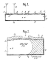
- a radiation detector embodying the invention consists of a circular wafer 1 of n-type silicon.
- One planar surface 2, the edge 3 and a peripheral annular region 4 of the other planar surface 5 are doped with phosphorus to produce a surface region 6 of n+ silicon and provide an n+n junction 6.
- the central region 7 of the surface 5 is doped with boron to produce a surface region 8 of p+ silicon and hence a p+n junction 8′.
- the annular region 9 between the peripheries of the n+n and p+n junctions is covered with an isolating annulus 10 of silicon dioxide.
- An annulus 11 and layer 12 of aluminium are deposited as shown to provide positive and negative contacts 13 and 14, respectively.
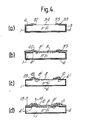
- the wafer 1 When the device is operated under conditions of reverse bias, the wafer 1 depletes from the surface 5 towards the surface 2, but as shown in figure 2, even when the main part of the wafer 1 is fully depleted, the region under the annular n+n region 4 does not deplete. As described previously, this renders the performance of the device insensitive to damage to the edge of the wafer 1.
- a wafer 1 of silicon is cleaned by any convenient process, such as are well known in the semiconductor art and therefore will not be described further, and is then oxidised in a dry/wet/dry oxidising process to produce an overall layer of silicon dioxide 31, as shown in figure 3(a). Again, such a process is well known in the semiconductor art.
- the layer 31 of silicon dioxide is then patterned by means of photolithography and wet chemical etching to leave a disk 32 of silicon dioxide, (as shown in figure 3b), on one face of the wafer 1 to act as a mask against phosphorus diffusion to create the low impedance wrap round n+n junction, which forms the next stage in the process.
- the phosphorus diffusion takes place from a layer of phosphosilicate glass 33 which is formed in situ by heating the wafer 1 to a temperature of 900°C in an atmosphere of phosphorus oxychloride (POCl3). This stage is illustrated in figure 3(c).
- the n+ layer 6 so formed will have a thickness of about 0.5 um and a sheet resistance of about 10 /square.
- a window 34 is then opened in the silicon dioxide mask 32 and the layer 33 of phosphosilicate glass 33 covering the surface 2, edge 3 and region 4 of the wafer 1 are removed in one wet chemical etching step, as shown in figure 3(d), after the annulus of silicon dioxide 32 which is to remain has been protected with photo-resist.
- the window 34 will have a bevelled edge 35 because the phosphosilicate glass 4 etches faster than silicon dioxide.
- the next step is to implant boron into the window region 34 defined by the annulus of silicon dioxide 32, as shown in figure 3(e).
- the bevelled edge 35 of the mask 32 has the beneficial effect of tapering the edge of the p+n junction 8′ which increases the junction breakdown voltage by reducing the electric field in the vicinity of the edge of the junction 8′ when the device is in use.
- the device is then annealed in dry nitrogen at 600°C for 30 minutes before a layer of aluminium is deposited on the whole of the back of the wafer 1. This layer of aluminium is then patterned by standard photolithographic techniques to leave an annulus 11 and a central disk 12 for the n+ silicon contact and the p+ silicon contact, respectively, as shown in figure 3(f).
- the device is then subjected to a final annealing stage in a mixture of nitrogen and hydrogen at 400°C.
- central aluminium disk 12 extends onto the silicon dioxide annulus 10 beyond the edge of the p+n junction 8′. This feature is an important factor in obtaining a high reverse breakdown voltage.
- FIG 4. A second process for the manufacture of a radiation detector embodying the invention is illustrated in figure 4.
- the first three stages in the process are as previously described and so will not be repeated. Instead of implanting boron to produce the rectifying junction, however, a spin-on dopant is used.
- First a window 41 is etched in the over-all layer of phosphosilicate glass 33 and the silicon dioxide mask 32 together, as shown in figure 4(a).
- the phosphosilicate glass layer 33 is left in place on the remainder of the wafer 1 to prevent counter doping of the edge 3 and annular region 4 of the wafer 1 with boron.
- a uniform layer of boric oxide is then deposited on the surface 5 of the wafer 1 by a spinning technique, again well-known in the semiconductor art, and fired to produce a layer 42 of borosilicate glass (figure 4(b).
- the layer 42 of borosilicate glass then acts as a source of boron to produce by diffusion of boron the heavily doped p+ surface region 8 and p+n junction 8′ in a manner analogous to that in which the n+ surface region 6 and n+n junction 6′ were produced.
- the wafer 1 is then heated to a temperature of 900°C for 60 minutes to produce a p+n junction depth of a few tenths of a micron and a p+ sheet resistance of about 100 /square.
- the boron drive-in stage above will also increase the depth of the high-low (n+n) junction 6′ under the layer of phosphosilicate glass 33 by a factor of 2.
- the majority of the layer of borosilicate glass 42 and the remainder of the layer of phosphosilicate glass 33 are then removed in a single wet etching step to leave the annulus of silicon dioxide 10 covered in both phosphosilicate and borosilicate glass, as shown in figure 4(c).
- the aluminium is deposited and patterned as before and the device annealed, also as before.
- Detectors made according to either of the above processes can be modified to make good alpha particle spectrometers. All that is required is to etch a window in the n+ layer of the surface 2 so as to remove this layer and then to implant arsenic to a dose of about 1013 ions per square millimetre at an energy of 30 keV. The device is then annealed to activate the implanted arsenic. This produces a shallow n+ layer which should represent a dead layer of about 50 nm only. Straggle of alpha particles through such a layer should produce an energy broadening of 4.5 keV fwhm.
- Detectors made by the second process which can withstand reverse bias voltages sufficient to produce an electric field strength of more than 103V mm ⁇ 1 throughout the depleted volume have potential for use as heavy ion detectors.
- the high value of electric field within the depleted volume of the wafer 1 is required to strip the dense electron-hole plasma created by highly ionising heavy ions before significant recombination of the electric charges so generated occurs.
Landscapes
- Light Receiving Elements (AREA)
- Measurement Of Radiation (AREA)
Applications Claiming Priority (2)
| Application Number | Priority Date | Filing Date | Title |
|---|---|---|---|
| GB888823246A GB8823246D0 (en) | 1988-10-04 | 1988-10-04 | Radiation detector |
| GB8823246 | 1988-10-04 |
Publications (2)
| Publication Number | Publication Date |
|---|---|
| EP0363069A2 true EP0363069A2 (fr) | 1990-04-11 |
| EP0363069A3 EP0363069A3 (fr) | 1990-09-12 |
Family
ID=10644675
Family Applications (1)
| Application Number | Title | Priority Date | Filing Date |
|---|---|---|---|
| EP19890309823 Withdrawn EP0363069A3 (fr) | 1988-10-04 | 1989-09-27 | Détecteur de radiation |
Country Status (3)
| Country | Link |
|---|---|
| EP (1) | EP0363069A3 (fr) |
| JP (1) | JPH02198176A (fr) |
| GB (2) | GB8823246D0 (fr) |
Cited By (2)
| Publication number | Priority date | Publication date | Assignee | Title |
|---|---|---|---|---|
| EP0581422A1 (fr) * | 1992-06-27 | 1994-02-02 | United Kingdom Atomic Energy Authority | Diode PIN utilisable comme dosimètre à neutrons |
| WO2013141700A3 (fr) * | 2012-03-20 | 2014-01-16 | Tempress Ip B.V. | Procédé de fabrication d'une cellule solaire |
Family Cites Families (3)
| Publication number | Priority date | Publication date | Assignee | Title |
|---|---|---|---|---|
| DE1764778A1 (de) * | 1968-08-03 | 1971-11-04 | Siemens Ag | Detektor zum Registrieren elektromagnetischer bzw. korpuskularer Strahlung und Verfahren zur Herstellung |
| US4361950A (en) * | 1980-03-24 | 1982-12-07 | Exxon Research & Engineering Co. | Method of making solar cell with wrap-around electrode |
| CA1182198A (fr) * | 1981-09-16 | 1985-02-05 | Paul P. Webb | Photodiode de si et methode d'obtention |
-
1988
- 1988-10-04 GB GB888823246A patent/GB8823246D0/en active Pending
-
1989
- 1989-09-26 GB GB8921685A patent/GB2223878B/en not_active Expired - Lifetime
- 1989-09-27 EP EP19890309823 patent/EP0363069A3/fr not_active Withdrawn
- 1989-10-04 JP JP1259870A patent/JPH02198176A/ja active Pending
Cited By (3)
| Publication number | Priority date | Publication date | Assignee | Title |
|---|---|---|---|---|
| EP0581422A1 (fr) * | 1992-06-27 | 1994-02-02 | United Kingdom Atomic Energy Authority | Diode PIN utilisable comme dosimètre à neutrons |
| WO2013141700A3 (fr) * | 2012-03-20 | 2014-01-16 | Tempress Ip B.V. | Procédé de fabrication d'une cellule solaire |
| US9224906B2 (en) | 2012-03-20 | 2015-12-29 | Tempress Ip B.V. | Method for manufacturing a solar cell |
Also Published As
| Publication number | Publication date |
|---|---|
| GB8823246D0 (en) | 1988-11-09 |
| GB2223878B (en) | 1992-01-02 |
| EP0363069A3 (fr) | 1990-09-12 |
| JPH02198176A (ja) | 1990-08-06 |
| GB8921685D0 (en) | 1989-11-08 |
| GB2223878A (en) | 1990-04-18 |
Similar Documents
| Publication | Publication Date | Title |
|---|---|---|
| US4104085A (en) | Method of manufacturing a semiconductor device by implanting ions through bevelled oxide layer in single masking step | |
| US3976511A (en) | Method for fabricating integrated circuit structures with full dielectric isolation by ion bombardment | |
| US4925807A (en) | Method of manufacturing a semiconductor device | |
| US4127932A (en) | Method of fabricating silicon photodiodes | |
| US3747203A (en) | Methods of manufacturing a semiconductor device | |
| US4201800A (en) | Hardened photoresist master image mask process | |
| US5719414A (en) | Photoelectric conversion semiconductor device with insulation film | |
| US4139402A (en) | Method of manufacturing a semiconductor device utilizing doped oxides and controlled oxidation | |
| US3849216A (en) | Method of manufacturing a semiconductor device and semiconductor device manufactured by using the method | |
| US5473184A (en) | Semiconductor device and method for fabricating same | |
| US4326211A (en) | N+PP-PP-P+ Avalanche photodiode | |
| US4018627A (en) | Method for fabricating semiconductor devices utilizing oxide protective layer | |
| EP0078725B1 (fr) | Procédé de fabrication de transistors bipolaires de dimensions inférieures au micron sans croissance épitaxiale et structure résultante | |
| CN110854222B (zh) | 一种漂移探测器的双面制备方法及漂移探测器 | |
| CN110854223B (zh) | 一种漂移探测器的制备方法及漂移探测器 | |
| EP0001139B1 (fr) | Diode à avalanche sensible aux rayonnements et son procédé de fabrication | |
| EP0363069A2 (fr) | Détecteur de radiation | |
| CA1078948A (fr) | Methode de fabrication de photodiodes au silicium | |
| US6225178B1 (en) | Radiation hardened field oxide for VLSI sub-micron MOS device | |
| JP3336734B2 (ja) | 素子分離領域の形成方法 | |
| US5021358A (en) | Semiconductor fabrication process using sacrificial oxidation to reduce tunnel formation during tungsten deposition | |
| CN108281480B (zh) | 一种同时产生电离和位移缺陷信号的器件及其制备方法 | |
| US4003759A (en) | Ion implantation of gold in mercury cadmium telluride | |
| EP0427285B1 (fr) | Procédé pour la fabrication d'un dispositif semi-conducteur à haute dureté de rayonnement | |
| US4353754A (en) | Thermo-sensitive switching element manufacturing method |
Legal Events
| Date | Code | Title | Description |
|---|---|---|---|
| PUAI | Public reference made under article 153(3) epc to a published international application that has entered the european phase |
Free format text: ORIGINAL CODE: 0009012 |
|
| AK | Designated contracting states |
Kind code of ref document: A2 Designated state(s): DE FR IT NL |
|
| PUAL | Search report despatched |
Free format text: ORIGINAL CODE: 0009013 |
|
| AK | Designated contracting states |
Kind code of ref document: A3 Designated state(s): DE FR IT NL |
|
| 17P | Request for examination filed |
Effective date: 19910312 |
|
| STAA | Information on the status of an ep patent application or granted ep patent |
Free format text: STATUS: THE APPLICATION IS DEEMED TO BE WITHDRAWN |
|
| 18D | Application deemed to be withdrawn |
Effective date: 19920401 |