EP0363084A2 - Déflecteur pour faisceau optique - Google Patents
Déflecteur pour faisceau optique Download PDFInfo
- Publication number
- EP0363084A2 EP0363084A2 EP89309919A EP89309919A EP0363084A2 EP 0363084 A2 EP0363084 A2 EP 0363084A2 EP 89309919 A EP89309919 A EP 89309919A EP 89309919 A EP89309919 A EP 89309919A EP 0363084 A2 EP0363084 A2 EP 0363084A2
- Authority
- EP
- European Patent Office
- Prior art keywords
- multiplicity
- window
- liquid crystal
- electrodes
- stripe electrodes
- Prior art date
- Legal status (The legal status is an assumption and is not a legal conclusion. Google has not performed a legal analysis and makes no representation as to the accuracy of the status listed.)
- Granted
Links
- 230000003287 optical effect Effects 0.000 title claims abstract description 77
- 239000004973 liquid crystal related substance Substances 0.000 claims abstract description 47
- 239000004020 conductor Substances 0.000 claims abstract description 19
- 229910052738 indium Inorganic materials 0.000 claims description 8
- APFVFJFRJDLVQX-UHFFFAOYSA-N indium atom Chemical compound [In] APFVFJFRJDLVQX-UHFFFAOYSA-N 0.000 claims description 8
- 238000005468 ion implantation Methods 0.000 claims description 7
- 210000002858 crystal cell Anatomy 0.000 abstract description 8
- 230000010363 phase shift Effects 0.000 abstract 1
- 239000010410 layer Substances 0.000 description 47
- 239000000758 substrate Substances 0.000 description 22
- 210000004027 cell Anatomy 0.000 description 21
- 238000000034 method Methods 0.000 description 14
- CURLTUGMZLYLDI-UHFFFAOYSA-N Carbon dioxide Chemical compound O=C=O CURLTUGMZLYLDI-UHFFFAOYSA-N 0.000 description 12
- JBRZTFJDHDCESZ-UHFFFAOYSA-N AsGa Chemical compound [As]#[Ga] JBRZTFJDHDCESZ-UHFFFAOYSA-N 0.000 description 7
- 238000000576 coating method Methods 0.000 description 7
- 229910052751 metal Inorganic materials 0.000 description 7
- 239000002184 metal Substances 0.000 description 7
- 229910002092 carbon dioxide Inorganic materials 0.000 description 6
- 239000001569 carbon dioxide Substances 0.000 description 6
- 239000010408 film Substances 0.000 description 6
- 230000008569 process Effects 0.000 description 6
- 229910001218 Gallium arsenide Inorganic materials 0.000 description 5
- 230000003667 anti-reflective effect Effects 0.000 description 5
- PCHJSUWPFVWCPO-UHFFFAOYSA-N gold Chemical group [Au] PCHJSUWPFVWCPO-UHFFFAOYSA-N 0.000 description 5
- 239000010931 gold Substances 0.000 description 5
- 229910052737 gold Inorganic materials 0.000 description 5
- WCUXLLCKKVVCTQ-UHFFFAOYSA-M Potassium chloride Chemical compound [Cl-].[K+] WCUXLLCKKVVCTQ-UHFFFAOYSA-M 0.000 description 4
- 239000005083 Zinc sulfide Substances 0.000 description 4
- 230000008878 coupling Effects 0.000 description 4
- 238000010168 coupling process Methods 0.000 description 4
- 238000005859 coupling reaction Methods 0.000 description 4
- 239000000463 material Substances 0.000 description 4
- 125000006850 spacer group Chemical group 0.000 description 4
- 229910052984 zinc sulfide Inorganic materials 0.000 description 4
- 239000006117 anti-reflective coating Substances 0.000 description 3
- 239000011248 coating agent Substances 0.000 description 3
- 229910003437 indium oxide Inorganic materials 0.000 description 3
- PJXISJQVUVHSOJ-UHFFFAOYSA-N indium(iii) oxide Chemical compound [O-2].[O-2].[O-2].[In+3].[In+3] PJXISJQVUVHSOJ-UHFFFAOYSA-N 0.000 description 3
- 230000000737 periodic effect Effects 0.000 description 3
- 239000004065 semiconductor Substances 0.000 description 3
- PFNQVRZLDWYSCW-UHFFFAOYSA-N (fluoren-9-ylideneamino) n-naphthalen-1-ylcarbamate Chemical compound C12=CC=CC=C2C2=CC=CC=C2C1=NOC(=O)NC1=CC=CC2=CC=CC=C12 PFNQVRZLDWYSCW-UHFFFAOYSA-N 0.000 description 2
- PNEYBMLMFCGWSK-UHFFFAOYSA-N aluminium oxide Inorganic materials [O-2].[O-2].[O-2].[Al+3].[Al+3] PNEYBMLMFCGWSK-UHFFFAOYSA-N 0.000 description 2
- 230000005540 biological transmission Effects 0.000 description 2
- 238000000151 deposition Methods 0.000 description 2
- 238000010586 diagram Methods 0.000 description 2
- 230000005684 electric field Effects 0.000 description 2
- 238000005516 engineering process Methods 0.000 description 2
- 229910052732 germanium Inorganic materials 0.000 description 2
- GNPVGFCGXDBREM-UHFFFAOYSA-N germanium atom Chemical compound [Ge] GNPVGFCGXDBREM-UHFFFAOYSA-N 0.000 description 2
- -1 halide salts Chemical class 0.000 description 2
- AMGQUBHHOARCQH-UHFFFAOYSA-N indium;oxotin Chemical compound [In].[Sn]=O AMGQUBHHOARCQH-UHFFFAOYSA-N 0.000 description 2
- 238000001465 metallisation Methods 0.000 description 2
- 235000011164 potassium chloride Nutrition 0.000 description 2
- 239000001103 potassium chloride Substances 0.000 description 2
- 238000003825 pressing Methods 0.000 description 2
- 239000002356 single layer Substances 0.000 description 2
- 238000001429 visible spectrum Methods 0.000 description 2
- DRDVZXDWVBGGMH-UHFFFAOYSA-N zinc;sulfide Chemical compound [S-2].[Zn+2] DRDVZXDWVBGGMH-UHFFFAOYSA-N 0.000 description 2
- 239000004593 Epoxy Substances 0.000 description 1
- 238000010521 absorption reaction Methods 0.000 description 1
- 230000001427 coherent effect Effects 0.000 description 1
- 238000013500 data storage Methods 0.000 description 1
- 230000008021 deposition Effects 0.000 description 1
- 239000003989 dielectric material Substances 0.000 description 1
- 238000005553 drilling Methods 0.000 description 1
- 238000000227 grinding Methods 0.000 description 1
- 150000004820 halides Chemical class 0.000 description 1
- 230000006872 improvement Effects 0.000 description 1
- 238000002329 infrared spectrum Methods 0.000 description 1
- 239000012212 insulator Substances 0.000 description 1
- 238000007737 ion beam deposition Methods 0.000 description 1
- 238000002955 isolation Methods 0.000 description 1
- 238000007648 laser printing Methods 0.000 description 1
- 239000007788 liquid Substances 0.000 description 1
- 238000004519 manufacturing process Methods 0.000 description 1
- 230000037230 mobility Effects 0.000 description 1
- 238000009304 pastoral farming Methods 0.000 description 1
- 229920002120 photoresistant polymer Polymers 0.000 description 1
- 238000001020 plasma etching Methods 0.000 description 1
- 230000010287 polarization Effects 0.000 description 1
- 239000000843 powder Substances 0.000 description 1
- 230000000644 propagated effect Effects 0.000 description 1
- 238000000992 sputter etching Methods 0.000 description 1
- 230000003068 static effect Effects 0.000 description 1
- 238000005728 strengthening Methods 0.000 description 1
- 239000010409 thin film Substances 0.000 description 1
- 239000012780 transparent material Substances 0.000 description 1
Images


Classifications
-
- G—PHYSICS
- G02—OPTICS
- G02F—OPTICAL DEVICES OR ARRANGEMENTS FOR THE CONTROL OF LIGHT BY MODIFICATION OF THE OPTICAL PROPERTIES OF THE MEDIA OF THE ELEMENTS INVOLVED THEREIN; NON-LINEAR OPTICS; FREQUENCY-CHANGING OF LIGHT; OPTICAL LOGIC ELEMENTS; OPTICAL ANALOGUE/DIGITAL CONVERTERS
- G02F1/00—Devices or arrangements for the control of the intensity, colour, phase, polarisation or direction of light arriving from an independent light source, e.g. switching, gating or modulating; Non-linear optics
- G02F1/29—Devices or arrangements for the control of the intensity, colour, phase, polarisation or direction of light arriving from an independent light source, e.g. switching, gating or modulating; Non-linear optics for the control of the position or the direction of light beams, i.e. deflection
- G02F1/292—Devices or arrangements for the control of the intensity, colour, phase, polarisation or direction of light arriving from an independent light source, e.g. switching, gating or modulating; Non-linear optics for the control of the position or the direction of light beams, i.e. deflection by controlled diffraction or phased-array beam steering
-
- G—PHYSICS
- G02—OPTICS
- G02F—OPTICAL DEVICES OR ARRANGEMENTS FOR THE CONTROL OF LIGHT BY MODIFICATION OF THE OPTICAL PROPERTIES OF THE MEDIA OF THE ELEMENTS INVOLVED THEREIN; NON-LINEAR OPTICS; FREQUENCY-CHANGING OF LIGHT; OPTICAL LOGIC ELEMENTS; OPTICAL ANALOGUE/DIGITAL CONVERTERS
- G02F1/00—Devices or arrangements for the control of the intensity, colour, phase, polarisation or direction of light arriving from an independent light source, e.g. switching, gating or modulating; Non-linear optics
- G02F1/01—Devices or arrangements for the control of the intensity, colour, phase, polarisation or direction of light arriving from an independent light source, e.g. switching, gating or modulating; Non-linear optics for the control of the intensity, phase, polarisation or colour
- G02F1/13—Devices or arrangements for the control of the intensity, colour, phase, polarisation or direction of light arriving from an independent light source, e.g. switching, gating or modulating; Non-linear optics for the control of the intensity, phase, polarisation or colour based on liquid crystals, e.g. single liquid crystal display cells
- G02F1/133—Constructional arrangements; Operation of liquid crystal cells; Circuit arrangements
- G02F1/1333—Constructional arrangements; Manufacturing methods
- G02F1/1345—Conductors connecting electrodes to cell terminals
-
- G—PHYSICS
- G02—OPTICS
- G02F—OPTICAL DEVICES OR ARRANGEMENTS FOR THE CONTROL OF LIGHT BY MODIFICATION OF THE OPTICAL PROPERTIES OF THE MEDIA OF THE ELEMENTS INVOLVED THEREIN; NON-LINEAR OPTICS; FREQUENCY-CHANGING OF LIGHT; OPTICAL LOGIC ELEMENTS; OPTICAL ANALOGUE/DIGITAL CONVERTERS
- G02F2201/00—Constructional arrangements not provided for in groups G02F1/00 - G02F7/00
- G02F2201/42—Arrangements for providing conduction through an insulating substrate
Definitions
- the present invention relates generally to optical systems and, more particularly, to an electrically tunable, optical phase shifter for use in an optical phased array antenna.
- a static deflector for deflecting a polarized infrared beam is disclosed in U.S. Patent No. 4,639,091, issued January 27, 1987, to J.-P. Huignard et al.
- the Huignard et al. deflector comprises a layered square plate having as a front layer a window on which stripe electrodes are disposed. Both the window and the stripe electrodes are transparent to an incident infrared beam.
- a middle layer of the deflector comprises an electro-optical liquid crystal layer.
- the bottom layer comprises a substrate having a common electrode adjacent the liquid crystal layer.
- the common electrode is preferably reflective at the beam wavelength, illustratively it is a gold film; alternatively, for a deflector operating by transmission, a transparent rear plate may be used.
- Huignard et al. discloses a periodic staircase waveform comprising N voltage steps which are applied to the stripe electrodes, thereby creating local variations of the refractive index in the liquid crystal layer in such a manner as to form a beam diffraction grating of adjustable period.
- the Huignard et al. patent discloses a deflector device comprising a plurality of stripe electrodes, but it fails to disclose an effective way of coupling control voltages to a very large number of stripe electrodes, wherein the electrodes are pitched in the order of the wavelength of light of interest, typically 0.2 to 14 micrometers. Applicants believe that, for the dimensions expressed in the Huignard et al. patent for stripe electrode widths and inter-electrode spacings, there does not currently exist a practical and realizable means for attaching independent control voltages to stripe electrodes which are spaced more densely than approximately 10-20 per millimeter.
- an optical phased array antenna used for rapid, phased-angle pointing and scanning of large diameter laser radar beams, as described earlier, would require a large multiplicity of stripe electrodes, and a correspondingly large plurality of means for coupling control voltages individually to those stripe electrodes.
- a one-half meter aperture phase shifter array operating on light having wavelength of 10 ⁇ meters, requires contacts for 100,000 electrodes, or 2,000 electrodes per centimeter. In order to operate the same phase shifter array at 1 ⁇ meter wavelength, contacts for one million electrodes would be required, or 20,000 electrodes per centimeter.
- the apparatus comprises an optical element including a first window having a transparent common electrode, a second window having a multiplicity of electrodes in the form of electrically-isolated parallel stripes, and a layer of liquid crystal molecules intermediate the first and second windows.
- the optical element is positioned so that the optical beam is incident on the first window, the beam being reflected from within the optical element.
- the apparatus further comprises means for generating a multiplicity of control signals, and means for applying the control signals individually between the multiplicity of stripe electrodes and the common electrode, thereby creating local variations of refractive index in the liquid crystal layer.
- the applying means preferably comprises an electrically-insulating layer affixed to the optical element opposite the first window; a multiplicity of electrically-conductive contact pads on an external surface of the insulating layer, each of the pads underlying a plurality of the stripe electrodes; and a multiplicity of conductors, each extending through the insulating layer for providing electrical conductivity between an individual stripe electrode and a corresponding contact pad.
- the parallel stripe electrodes are optically transparent, and the incident optical beam passes through these electrodes and the insulating layer, and is reflected from the closely-spaced, metallic contact pads thereunder.
- the parallel stripe electrodes are optically reflective, and the incident optical beam is reflected therefrom.
- the phase shifter includes an optical subsystem 10 and an electronics module 16.
- Optical subsystem 10 includes an optically-transparent common electrode 12, a multiplicity of stripe electrodes 14a, 14b, ..., 14j, and a layer of liquid crystal molecules 13 therebetween.
- Electronics module 16 supplies appropriate control signals to electrodes 14a, 14b, ..., 14j, referred to collectively as electrodes 14, via conductors 15a, 15b, ..., 15j, referred to collectively as conductors 15, respectively (only conductors 15a, 15e and 15i are visible in FIG. 1).
- the optical beam phase shifter of FIG. 1 is responsive to a light source and beam forming network (not shown) which provide a polarized, coherent light beam, typically in the infrared spectrum, having a typical wavelength in the range of 9 to 11.5 ⁇ meters ( ⁇ m), illustratively at 10.6 ⁇ m.
- the light beam represented in part by rays 18a, 18b and 18c, is directed obliquely onto the upper surface 11 of optical subsystem 10 such that its projection onto the plane formed by stripe electrodes 14 is parallel to the direction of electrodes 14.
- the longitudinal edges of stripe electrodes 14 are parallel to the planes of incidence of rays 18a, 18b and 18c.
- the potentials applied to the electrodes 14 onto which rays 18a, 18b and 18c are incident are such as to cause the greatest retardation to reflected ray 19c, and the least retardation to reflected ray 19a.
- the wavefront 17 of the beam reflected from within the optical beam deflector appears to be deflected from the normal plane of incidence/reflection. It is therefore seen that the optical beam deflector of FIG. 1 provides selective beam steering in accordance with the electrical potentials applied to stripe electrodes 14.
- control voltage signals to the individual stripe electrodes 14 for the purpose of beam steering is analogous to the methods used in conventional microwave radar beam steering as taught, for example, in Radar Handbook , M.I. Skolnik, ed., McGraw-Hill, New York, 1970, at chapter 11.
- a plurality of control voltage signals being periodic in space and having a continuous progression of voltage steps within each period between a minimum value and a maximum value, may be applied to the multiplicity of stripe electrodes l4.
- the parallel stripe electrodes are substantially optically transparent, and the incident light beam passes through these electrodes and is reflected by a discontinuous optically-reflective layer thereunder comprising a plane of closely-spaced metallic contact pads.
- the narrow spacing between the contact pads is minimized in order to minimize any extraneous grating patterns which may exist.
- the parallel stripe electrodes are optically reflective, and the incident light beam is reflected therefrom. In this second embodiment, the narrow spacing between the stripe electrodes is minimized in order to minimize a fixed secondary grating which may exist.
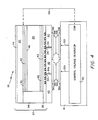
- FIGS. 2 and 3 there is shown, respectively, a plan view and a sectional view of the optical subsystem 10 of the optical beam deflector of FIG. 1. It will be recognized that no effort has been made to provide accurate scale to FIGS. 2 and 3, and that some dimensions are highly exaggerated in order to clearly depict all of the structural elements.
- the optical subsystem 10 of the optical phase shifter of the present embodiment comprises a liquid crystal cell 20 affixed to an electrically-insulating layer 40.
- Liquid crystal cell 20 comprises a first window 22, a second window 26, spacer 28 maintaining a fixed spacing between windows 22 and 26, and a layer 24 of liquid crystal molecules in the space between windows 22 and 26.
- Window 22 includes optically-transparent common electrode 30, and window 26 includes a plurality of optically-transparent electrodes 32a, 32b, ..., 32l, referred to collectively as electrodes 32, in the form of electrically-isolated parallel stripes.
- electrodes 32 may be 4-10 ⁇ meters in width, and spaced from one another by approximately one ⁇ meter.
- Electrically-insulating layer 40 which may illustratively be fabricated of a dielectric material such as zinc sulfide (ZnS) or semi-insulating gallium arsenide (GaAs), provides electrical isolation between electrodes 32 and the metallic contact pads (to be described below). It is a requirement that the material of insulating layer 40 be substantially optically transparent at the wavelength of the light as described.
- An anti-reflection coating 44 is affixed to the external surface of window 22, and anti-reflection coatings 42 and 43 are affixed, respectively, to the inner surfaces of windows 22 and 26.
- Alignment layers 46 and 48 are interposed between the layer 24 of liquid crystal molecules and cell windows 22 and 26, respectively, to properly align the liquid crystal molecules at the boundaries of layer 24.
- the alignment of the liquid crystal molecules is selected to be appropriate to the polarization of the incident light such that liquid crystal cell 20 functions properly as a switch. It has been determined that a preferable alignment of the liquid crystal molecules is orthogonal to the longitudinal edges of the stripe electrodes 32. The presence of the inevitable fringing fields between electrodes 32 will reinforce the original molecular alignment established by the alignment layers 46 and 48.
- Conductors 34a, 34b, ..., 34l, referred to collectively as conductors 34 provide electrical paths between electrodes 32 and pads 36a, 36b, ..., 36l, referred to collectively as pads 36 (only 36c and 36i are shown in FIG. 3), through insulating layer 40.
- Each individual pad 36 includes a protrusion or "bump" 38a, 38b, ..., 38l, referred to collectively as bumps 38 (only 38c and 38i are shown in FIG. 3), to be used for bonding to an individual source of control voltage, in a manner to be described hereinafter.
- cell windows 22 and 26 must exhibit low absorption of the infrared light having the wavelength emitted by a CO2 laser, typically at 10.6 ⁇ m.
- Typical candidates for the choice of cell windows 22 and 26 include semiconductors such as germanium, zinc selenide and gallium arsenide, and halide salts such as potassium chloride, all of which are relatively transparent to CO2 laser light.
- electrode 30, which provides electrical conductivity across cell window 22, and electrodes 32, which provide a multiplicity of individual zones of electrical conductivity on cell window 26, must also be substantially optically transparent at the above-mentioned wavelength.
- an optically transparent electrode by the deposition of a thin-film conductor, such as indium-tin oxide (ITO) or indium oxide (In2O3), on a surface of a plate of transparent material.
- ITO indium-tin oxide
- In2O3 indium oxide
- Such conductive films are inherently lossy in the infrared region, that is, they absorb the infrared energy, due to their high electron concentrations and low carrier mobilities.
- An indium-tin oxide film a few thousand Angstroms-thick transmits approximately 80-90 percent in the visible spectrum, and a 200 Angstrom-thick film transmits approximately 50 percent at a wavelength of 10.6 ⁇ m.
- lt has been reported that indium oxide provides 65-80 percent transmission at wavelengths between 8-12 ⁇ m with film sheet resistances of 20-50 ohms/square.
- optically transparent electrodes 30 and 32 are preferably provided on cell windows 22 and 26 by a process of ion implantation, as disclosed in European Patent Application No. 89302040.4, publication No. 0331462.
- Anti-reflective layers 42, 43 and 44 reduce the reflections when light passes from one optically-transmissive medium to another.
- Single layer and multiple anti-reflective coatings are well known in the art and are used to effectively eliminate reflections.
- a single layer anti-reflective coating comprises a material whose refractive index is the geometric mean of the refractive indices of the two media to be matched.
- the refractive indices of cell windows 22 and 26 and the liquid crystal molecules of layer 24 may be sufficiently close that inner anti-reflective layers 42 and 43 are not necessary.
- the liquid crystals In order to exhibit the desired birefringence in bulk devices, the liquid crystals must be properly and uniformly aligned. This is usually done by special treatment of the surfaces of cell windows 22 and 26 adjacent layer 24. If the inner surfaces of cell windows 22 and 26 have been "prepared” or striolated by, for example, rubbing unidirectionally with fine grinding powder to produce extremely fine, parallel striolae, the liquid crystal molecules of layer 24 adjacent to the inner surfaces of cell windows 22 and 26 will tend to align themselves along and in these minute grooves and thereby be preferentially aligned.
- the liquid crystal molecules of layer 24 within cell 20 are, illustratively, long, thin, rod-like organic molecules of the so-called "nematic" phase. These molecules exhibit long range molecular order in the liquid state.
- FIG. 2 shows most advantageously the relationships between electrodes 32, conductors 34 and pads 36. Since it is clear that for the widths of electrodes 32 expressed above, there exists no practical and realizable method in the state-of-the-art to affix individual leads to each of a great number of such electrodes, the present invention discloses relatively large contact pads 36 underlying stripe electrodes 32, and whose widths span a number of stripe electrodes 32, illustratively six in the present example. In the present embodiment, it is a requirement that contact pads 36 be as closely-spaced as is practicable, since the surface of the totality of pads adjacent insulating layer 40 forms the reflective surface for the reflection of the incident light beam.
- Contact pads 36 are preferably made of gold. Each pad 36 is electrically coupled to a single electrode 32 by a conductor 34, which may typically be deposited into a via hole. Conductors 34 are typically spaced apart in the staggered configuration as shown in FIG. 2. The via holes into which conductors 34 are deposited may typically have a diameter of 0.5-1.0 ⁇ meter.
- Bumps 38 typically substantially round, convex deposits of indium, are deposited on pads 36.
- Bumps 38 preferably have a diameter slightly less than the length of a side of pad 36, so that when bumps 38 are "welded" by the application of pressure between corresponding bumps, they may expand slightly without being shorted to one another.
- An illustrative process for fabricating the optical subsystem 10 according to this embodiment includes ion implantation of the stripe electrodes in a gallium arsenide wafer, typically in accordance with the teachings of Patent Application No. 89302040.4.
- the electrode side of the wafer is then coated with a dielectric, for example, ZnS or Y2O3, to a thickness of between a few hundred Angstroms and several ⁇ meters, i.e., just enough to provide a good insulator.
- Via holes are formed through the insulating layer using, for example, E-beam photoresist technology for best resolution.
- the external surface of the insulating layer is overcoated with a conductor, typically gold, ensuring that the conductor fills the via holes so as to make contact with the implanted electrodes.
- the gold is then etched to form the individual contact pads, and indium bumps are deposited on each contact pad.
- the wafer After “bumping" the GaAs wafer to the electronics module (as described hereinafter) and backfilling the assembly with strengthening epoxy, the wafer is turned over and the GaAs is lapped down to a very thin layer, illustratively one ⁇ meter. The lapped surface is polished and one or more anti-reflective coatings are applied. Over this, an alignment layer is applied, and the liquid crystal cell is then assembled, including spacers, the remaining cell window including the common electrode, anti-reflection coatings, and liquid crystal molecules, according to known techniques.
- Electronics module 16 includes a control voltage generator 50, which applies selectable voltages to each of a large plurality of output ports, which ports are coupled via signal leads (represented in FIG. 4 by leads 52c, 52i) to a corresponding large plurality of contact pads (represented in FIG. 4 by pads 56c, 56i) on an outer surface of electronics module 16.
- Each of the contact pads 56 on electronics module 16 corresponds in position to a contact pad 36 on optical subsystem 10.
- Each contact pad 56c, 56i on electronics module 16 includes a bump (represented in FIG. 4 by bumps 58c, 58i), typically a substantially round, convex deposit of indium, each bump 58c, 58i corresponding in position to a bump (represented in FIG. 4 by bumps 38c, 38i) on optical subsystem 10.
- Fabrication of the optical beam phase shifter of the present invention is completed by positioning optical subsystem 10 and electronics module 16 so that bumps 38 and 58 are aligned, and elements 10 and 16 are urged together under sufficient pressure to cause the pairs of indium bumps 38 and 58 to be welded.
- the control voltage circuit is completed by connection of the common voltage output port (COM) of control signal generator 50 to the common electrode 30 of optical subsystem 10 via lead 54.
- COM common voltage output port
- optical beam deflectors which relate the sizes of the substrate to the spacings between the metal contact pads.
- the substrate will contain 1250 electrode stripes.
- An array of approximately 35-by-35 contact pads will be required at the bottom surface of the substrate, which array will occur on 283 ⁇ meter centers in two dimensions.
- the substrate will contain 12,500 electrode stripes, for the same electrode pitch as above.
- an array of approximately 112-by-112 contact pads wi11 be required at the bottom of the substrate, which array will occur on 894 ⁇ meter centers in two dimensions. It is therefore seen that as the substrate size increases, the linear dimensions available for each contact pad increases by the square root of the linear factor of substrate size increase.
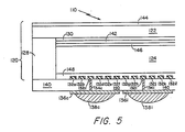
- FIG. 5 there is shown a cross-sectional view of a second embodiment of the optical subsystem of the optical beam deflector of the present invention.
- This embodiment is characterized in that the parallel stripe electrodes are optically reflective, and the incident light beams are reflected therefrom, obviating the need for a separate reflection layer, as in the FIGS. 2-3 embodiment.
- Optical subsystem 110 comprises a liquid crystal cell 120 including a window 122, spacer 128 maintaining a fixed spacing between window 122 and insulating substrate 140, and a layer 124 of liquid crystal molecules in the space between window 122 and insulating substrate 140.
- Window 122 includes an optically-transparent common electrode 130
- insulating substrate 140 includes a multiplicity of optically-reflective electrodes 132a, 132b, ..., 132l, referred to collectively as electrodes 132, in the form of closely-spaced electrically-isolated parallel stripes.
- electrodes 132 may be 4-10 ⁇ meters in width, and spaced from one another by approximately one ⁇ meter.
- Anti-reflection coatings 142 and 144 are affixed, respectively, to the internal and external surfaces of window 122.
- Alignment layers 146 and 148 are interposed between the layer 124 of liquid crystal molecules and cell window 122 and optically-reflective electrodes 132, respectively, to properly align the liquid crystal molecules at the boundaries of layer 124.
- Conductors 134 (only 134c and 134i are shown in the view of FIG. 5) provide electrical paths between electrodes 132 and contact pads 136 (only 136c and 136i are shown in FIG. 5), through insulating substrate 140.
- Each individual contact pad 136 includes a protrusion or bump 138 (only 138a and 138i are shown in FIG. 5), to be used for bonding to an individual source of control voltage, in a manner substantially identical to that described in relation to the embodiment of FIGS. 2-3.
- common electrode 130 is preferably fabricated according to the process described in the referenced patent application, Serial No. 162,922, and the metal reflective electrodes are illustratively fabricated using a metal deposition process.
- the use of anti-reflection layers 142 and 144, and alignment layers 146 and 148 is governed by the same principles described in relation to the embodiment of FIGS. 2-3.
- the process for fabricating the optical subsystem 110 includes providing metal contact pads to be used as the electrodes for the application of the individual control voltages on an insulating substrate, such as alumina or gallium arsenide (GaAs). Via holes are then formed through the substrate to the metal contact pads using, illustratively, laser drilling, for the case of an alumina substrate, or techniques such as ion milling and reactive ion etching, for the case of a GaAs substrate. The via holes may be filled using a selective metal deposition technique.
- an insulating substrate such as alumina or gallium arsenide (GaAs).
- Via holes are then formed through the substrate to the metal contact pads using, illustratively, laser drilling, for the case of an alumina substrate, or techniques such as ion milling and reactive ion etching, for the case of a GaAs substrate.
- the via holes may be filled using a selective metal deposition technique.
- Reflective, conductive metal stripe electrodes are then deposited on the surface of the insulating substrate opposite the surface having contact pads, each stripe making electrical contact with the fill metal of a single via hole.
- An alignment layer for the liquid crystal molecules is deposited over the stripe electrodes, and the liquid crystal cell is then assembled, including spacers, cell windows, anti-reflection coatings, and liquid crystal molecules, according to known techniques. It will be recognized that the indium bumps may be applied to the metal contact pads at virtually any point in this process.
Landscapes
- Physics & Mathematics (AREA)
- Nonlinear Science (AREA)
- General Physics & Mathematics (AREA)
- Optics & Photonics (AREA)
- Mathematical Physics (AREA)
- Chemical & Material Sciences (AREA)
- Crystallography & Structural Chemistry (AREA)
- Liquid Crystal (AREA)
Applications Claiming Priority (2)
| Application Number | Priority Date | Filing Date | Title |
|---|---|---|---|
| US07/253,021 US4964701A (en) | 1988-10-04 | 1988-10-04 | Deflector for an optical beam |
| US253021 | 1988-10-04 |
Publications (3)
| Publication Number | Publication Date |
|---|---|
| EP0363084A2 true EP0363084A2 (fr) | 1990-04-11 |
| EP0363084A3 EP0363084A3 (fr) | 1991-05-02 |
| EP0363084B1 EP0363084B1 (fr) | 1995-05-24 |
Family
ID=22958515
Family Applications (1)
| Application Number | Title | Priority Date | Filing Date |
|---|---|---|---|
| EP89309919A Expired - Lifetime EP0363084B1 (fr) | 1988-10-04 | 1989-09-28 | Déflecteur pour faisceau optique |
Country Status (2)
| Country | Link |
|---|---|
| US (1) | US4964701A (fr) |
| EP (1) | EP0363084B1 (fr) |
Cited By (6)
| Publication number | Priority date | Publication date | Assignee | Title |
|---|---|---|---|---|
| EP0642051A3 (fr) * | 1993-09-03 | 1995-09-20 | Hughes Aircraft Co | Séparateur optique reconfigurable et son procédé de fonctionnement. |
| WO1999024866A1 (fr) * | 1997-11-05 | 1999-05-20 | Zhu, Runshu | Dispositif a reseau de phase optique et procede de realisation |
| FR2788863A1 (fr) * | 1999-01-22 | 2000-07-28 | France Telecom | Support pour dispositif d'aiguillage optique |
| EP0977077A3 (fr) * | 1998-07-28 | 2001-04-04 | Nippon Telegraph and Telephone Corporation | Dispositif optique et appareil d'affichage |
| US6819393B1 (en) | 1998-07-28 | 2004-11-16 | Nippon Telegraph And Telephone Corporation | Optical device and display apparatus using light diffraction and light guide |
| CN109932850A (zh) * | 2018-03-29 | 2019-06-25 | 京东方科技集团股份有限公司 | 电子开关和遥控钥匙 |
Families Citing this family (87)
| Publication number | Priority date | Publication date | Assignee | Title |
|---|---|---|---|---|
| FR2650400B1 (fr) * | 1989-07-25 | 1991-10-04 | Thomson Csf | Deflecteur electro-optique a cristal liquide |
| US5126869A (en) * | 1990-12-03 | 1992-06-30 | Raytheon Company | Two-dimensional, phased-array optical beam steerer |
| US5107357A (en) * | 1991-01-18 | 1992-04-21 | General Electric Company | Low insertion loss optical beam steerer |
| US5093747A (en) * | 1991-02-28 | 1992-03-03 | Raytheon Company | Method for providing beam steering in a subaperture-addressed optical beam steerer |
| US5093740A (en) * | 1991-02-28 | 1992-03-03 | Raytheon Company | Optical beam steerer having subaperture addressing |
| EP0506422A1 (fr) * | 1991-03-29 | 1992-09-30 | Raytheon Company | Dispositif de transmission optique ayant des électrodes |
| JPH0764123A (ja) * | 1993-08-20 | 1995-03-10 | Internatl Business Mach Corp <Ibm> | 屈折率分布型光偏向器及び光偏向方法 |
| US5440654A (en) * | 1993-12-30 | 1995-08-08 | Raytheon Company | Fiber optic switching system |
| US6704474B1 (en) | 1994-05-24 | 2004-03-09 | Raytheon Company | Optical beam steering system |
| US5594565A (en) * | 1994-12-02 | 1997-01-14 | General Electric Company | Programmable liquid crystal wavefront device |
| US5827622A (en) * | 1995-11-02 | 1998-10-27 | International Business Machines Corporation | Reflective lithographic mask |
| US5943159A (en) * | 1996-05-14 | 1999-08-24 | Zhu; Tom Yuxin | Method and apparatus for optical beam steering |
| US6552321B1 (en) | 2000-09-01 | 2003-04-22 | Raytheon Company | Adaptive spectral imaging device and method |
| US6490076B2 (en) | 2001-01-11 | 2002-12-03 | Hrl Laboratories, Llc | Optical phased array for depolarized optical beam control |
| GB0121308D0 (en) | 2001-09-03 | 2001-10-24 | Thomas Swan & Company Ltd | Optical processing |
| US6832028B2 (en) * | 2002-10-08 | 2004-12-14 | Innovative Technology Licensing, Llc | Liquid crystal adaptive coupler for steering a light beam relative to a light-receiving end of an optical waveguide |
| JP2006085837A (ja) | 2004-09-16 | 2006-03-30 | Konica Minolta Opto Inc | 対物レンズユニット及びこれを用いた光ピックアップ装置 |
| US7372610B2 (en) | 2005-02-23 | 2008-05-13 | Sage Electrochromics, Inc. | Electrochromic devices and methods |
| GB0522968D0 (en) | 2005-11-11 | 2005-12-21 | Popovich Milan M | Holographic illumination device |
| GB0718706D0 (en) | 2007-09-25 | 2007-11-07 | Creative Physics Ltd | Method and apparatus for reducing laser speckle |
| US20080031627A1 (en) * | 2006-08-04 | 2008-02-07 | Smith Irl W | Optical communication system |
| US8116632B2 (en) * | 2007-11-30 | 2012-02-14 | Raytheon Company | Space-time division multiple-access laser communications system |
| US7940457B2 (en) * | 2008-05-30 | 2011-05-10 | The Board Of Trustees Of The University Of Illinois | Energy-efficient optoelectronic smart window |
| US8059254B1 (en) | 2008-06-04 | 2011-11-15 | Raytheon Company | Transparent heatsink/structure/interconnect for tiling space based optical components |
| US9335604B2 (en) | 2013-12-11 | 2016-05-10 | Milan Momcilo Popovich | Holographic waveguide display |
| US11726332B2 (en) | 2009-04-27 | 2023-08-15 | Digilens Inc. | Diffractive projection apparatus |
| US11204540B2 (en) | 2009-10-09 | 2021-12-21 | Digilens Inc. | Diffractive waveguide providing a retinal image |
| US20200057353A1 (en) | 2009-10-09 | 2020-02-20 | Digilens Inc. | Compact Edge Illuminated Diffractive Display |
| KR101147416B1 (ko) * | 2010-07-26 | 2012-05-23 | 삼성모바일디스플레이주식회사 | 표시 장치 |
| US8553225B2 (en) | 2010-07-29 | 2013-10-08 | Raytheon Company | Bandwidth tunable spectroscopic device |
| US8294879B2 (en) | 2010-11-15 | 2012-10-23 | Raytheon Company | Multi-directional active sensor |
| US9274349B2 (en) | 2011-04-07 | 2016-03-01 | Digilens Inc. | Laser despeckler based on angular diversity |
| US9045933B2 (en) | 2011-06-06 | 2015-06-02 | The Board Of Trustees Of The University Of Illinois | Energy-efficient smart window system |
| EP2748670B1 (fr) | 2011-08-24 | 2015-11-18 | Rockwell Collins, Inc. | Affichage de données portable |
| US10670876B2 (en) | 2011-08-24 | 2020-06-02 | Digilens Inc. | Waveguide laser illuminator incorporating a despeckler |
| WO2016020630A2 (fr) | 2014-08-08 | 2016-02-11 | Milan Momcilo Popovich | Illuminateur laser en guide d'ondes comprenant un dispositif de déchatoiement |
| US20150010265A1 (en) | 2012-01-06 | 2015-01-08 | Milan, Momcilo POPOVICH | Contact image sensor using switchable bragg gratings |
| EP2842003B1 (fr) | 2012-04-25 | 2019-02-27 | Rockwell Collins, Inc. | Affichage grand angle holographique |
| US9456744B2 (en) | 2012-05-11 | 2016-10-04 | Digilens, Inc. | Apparatus for eye tracking |
| WO2013177514A1 (fr) | 2012-05-24 | 2013-11-28 | Raytheon Company | Combinateur cohérent pour faisceaux de grande puissance |
| GB2504970A (en) | 2012-08-15 | 2014-02-19 | Swan Thomas & Co Ltd | Optical device and methods to reduce cross-talk |
| US9933684B2 (en) | 2012-11-16 | 2018-04-03 | Rockwell Collins, Inc. | Transparent waveguide display providing upper and lower fields of view having a specific light output aperture configuration |
| US10209517B2 (en) | 2013-05-20 | 2019-02-19 | Digilens, Inc. | Holographic waveguide eye tracker |
| NZ713761A (en) | 2013-05-24 | 2017-05-26 | Raytheon Co | Adaptive-optic having meander resistors |
| US9727772B2 (en) | 2013-07-31 | 2017-08-08 | Digilens, Inc. | Method and apparatus for contact image sensing |
| WO2016020632A1 (fr) | 2014-08-08 | 2016-02-11 | Milan Momcilo Popovich | Procédé pour gravure par pressage et réplication holographique |
| WO2016042283A1 (fr) | 2014-09-19 | 2016-03-24 | Milan Momcilo Popovich | Procédé et appareil de production d'images d'entrée pour affichages à guides d'ondes holographiques |
| EP3198192A1 (fr) | 2014-09-26 | 2017-08-02 | Milan Momcilo Popovich | Dispositif de poursuite optique à guide d'ondes holographique |
| US10437064B2 (en) | 2015-01-12 | 2019-10-08 | Digilens Inc. | Environmentally isolated waveguide display |
| EP3245551B1 (fr) | 2015-01-12 | 2019-09-18 | DigiLens Inc. | Afficheurs à champ lumineux et à guide d'ondes |
| CN107533137A (zh) | 2015-01-20 | 2018-01-02 | 迪吉伦斯公司 | 全息波导激光雷达 |
| US9632226B2 (en) | 2015-02-12 | 2017-04-25 | Digilens Inc. | Waveguide grating device |
| WO2016146963A1 (fr) | 2015-03-16 | 2016-09-22 | Popovich, Milan, Momcilo | Dispositif de guide d'onde incorporant un conduit de lumière |
| US10591756B2 (en) | 2015-03-31 | 2020-03-17 | Digilens Inc. | Method and apparatus for contact image sensing |
| US9620855B2 (en) | 2015-07-20 | 2017-04-11 | Elwha Llc | Electromagnetic beam steering antenna |
| US9577327B2 (en) * | 2015-07-20 | 2017-02-21 | Elwha Llc | Electromagnetic beam steering antenna |
| WO2017060665A1 (fr) | 2015-10-05 | 2017-04-13 | Milan Momcilo Popovich | Afficheur à guide d'ondes |
| EP3398007B1 (fr) | 2016-02-04 | 2024-09-11 | DigiLens, Inc. | Dispositif de poursuite optique de guide d'onde |
| JP6895451B2 (ja) | 2016-03-24 | 2021-06-30 | ディジレンズ インコーポレイテッド | 偏光選択ホログラフィー導波管デバイスを提供するための方法および装置 |
| EP3433658B1 (fr) | 2016-04-11 | 2023-08-09 | DigiLens, Inc. | Dispositif guide d'onde pour la projection de lumiere structuree |
| EP3548939A4 (fr) | 2016-12-02 | 2020-11-25 | DigiLens Inc. | Dispositif de guide d'ondes à éclairage de sortie uniforme |
| US10359623B2 (en) * | 2016-12-16 | 2019-07-23 | Wisconsin Alumni Research Foundation | Optical phase shifter |
| US10545346B2 (en) | 2017-01-05 | 2020-01-28 | Digilens Inc. | Wearable heads up displays |
| CN111386495B (zh) | 2017-10-16 | 2022-12-09 | 迪吉伦斯公司 | 用于倍增像素化显示器的图像分辨率的系统和方法 |
| CN114721242B (zh) | 2018-01-08 | 2025-08-15 | 迪吉伦斯公司 | 用于制造光学波导的方法 |
| JP7456929B2 (ja) | 2018-01-08 | 2024-03-27 | ディジレンズ インコーポレイテッド | 導波管セルを製造するためのシステムおよび方法 |
| JP7404243B2 (ja) | 2018-01-08 | 2023-12-25 | ディジレンズ インコーポレイテッド | 導波管セル内のホログラフィック格子の高スループット記録のためのシステムおよび方法 |
| WO2019136476A1 (fr) | 2018-01-08 | 2019-07-11 | Digilens, Inc. | Architectures de guides d'ondes et procédés de fabrication associés |
| US10690851B2 (en) | 2018-03-16 | 2020-06-23 | Digilens Inc. | Holographic waveguides incorporating birefringence control and methods for their fabrication |
| US11402801B2 (en) | 2018-07-25 | 2022-08-02 | Digilens Inc. | Systems and methods for fabricating a multilayer optical structure |
| US11121302B2 (en) | 2018-10-11 | 2021-09-14 | SeeQC, Inc. | System and method for superconducting multi-chip module |
| CN109164662B (zh) * | 2018-10-23 | 2023-08-22 | 长春理工大学 | 基于液晶光学相控阵的光束偏转控制方法 |
| WO2020149956A1 (fr) | 2019-01-14 | 2020-07-23 | Digilens Inc. | Affichage de guide d'ondes holographique avec couche de commande de lumière |
| US20200247017A1 (en) | 2019-02-05 | 2020-08-06 | Digilens Inc. | Methods for Compensating for Optical Surface Nonuniformity |
| EP3924759B1 (fr) | 2019-02-15 | 2025-07-30 | Digilens Inc. | Procédés et appareils pour fournir un affichage de guide d'ondes holographique à l'aide de réseaux intégrés |
| US20220283377A1 (en) | 2019-02-15 | 2022-09-08 | Digilens Inc. | Wide Angle Waveguide Display |
| JP2022525165A (ja) | 2019-03-12 | 2022-05-11 | ディジレンズ インコーポレイテッド | ホログラフィック導波管バックライトおよび関連する製造方法 |
| EP3980825A4 (fr) | 2019-06-07 | 2023-05-03 | Digilens Inc. | Guides d'ondes incorporant des réseaux transparents et réfléchissants et procédés de fabrication associés |
| JP2022543571A (ja) | 2019-07-29 | 2022-10-13 | ディジレンズ インコーポレイテッド | 画素化されたディスプレイの画像解像度および視野を乗算するための方法および装置 |
| JP2022546413A (ja) | 2019-08-29 | 2022-11-04 | ディジレンズ インコーポレイテッド | 真空回折格子および製造方法 |
| CN112731715B (zh) * | 2019-10-14 | 2022-11-11 | 京东方科技集团股份有限公司 | 液晶移相器及天线 |
| KR102778266B1 (ko) * | 2019-10-18 | 2025-03-11 | 현대자동차주식회사 | 액정 기반 광 편향기 및 이를 이용한 광 스캐너 |
| CN111290181B (zh) * | 2019-10-23 | 2022-08-19 | 南方科技大学 | 自动寻址激光扫描电极结构、控制方法以及制造方法 |
| CN113867019B (zh) * | 2020-06-30 | 2024-05-07 | 成都天马微电子有限公司 | 液晶移相器以及制作方法 |
| EP4252048A4 (fr) | 2020-12-21 | 2024-10-16 | Digilens Inc. | Suppression de la luminescence de l'oeil dans des affichages à base de guide d'ondes |
| WO2022150841A1 (fr) | 2021-01-07 | 2022-07-14 | Digilens Inc. | Structures de réseau pour guides d'ondes de couleur |
| KR20230153459A (ko) | 2021-03-05 | 2023-11-06 | 디지렌즈 인코포레이티드. | 진공 주기적 구조체 및 제조 방법 |
Family Cites Families (7)
| Publication number | Priority date | Publication date | Assignee | Title |
|---|---|---|---|---|
| FR2134160B1 (fr) * | 1971-04-22 | 1975-01-17 | Commissariat Energie Atomique | |
| US3915548A (en) * | 1973-04-30 | 1975-10-28 | Hughes Aircraft Co | Holographic lens and liquid crystal image source for head-up display |
| US4066334A (en) * | 1975-01-06 | 1978-01-03 | National Research Development Corporation | Liquid crystal light deflector |
| FR2541784B1 (fr) * | 1983-02-25 | 1986-05-16 | Thomson Csf | Dispositif de deflexion statique d'un faisceau infra-rouge |
| DE3851623T2 (de) * | 1987-08-19 | 1995-02-09 | Hughes Aircraft Co | Phasengesteuerter lichtablenker. |
| US4824215A (en) * | 1988-01-22 | 1989-04-25 | Xtalite Technology Limited/La Technologie Xtalite Limitee | Liquid crystal display apparatus |
| US4882235A (en) * | 1988-03-02 | 1989-11-21 | Raytheon Company | Liquid crystal cell window |
-
1988
- 1988-10-04 US US07/253,021 patent/US4964701A/en not_active Expired - Lifetime
-
1989
- 1989-09-28 EP EP89309919A patent/EP0363084B1/fr not_active Expired - Lifetime
Cited By (10)
| Publication number | Priority date | Publication date | Assignee | Title |
|---|---|---|---|---|
| EP0642051A3 (fr) * | 1993-09-03 | 1995-09-20 | Hughes Aircraft Co | Séparateur optique reconfigurable et son procédé de fonctionnement. |
| US5650835A (en) * | 1993-09-03 | 1997-07-22 | Hughes Electronics | Reconfigurable optical beam splitter and method |
| WO1999024866A1 (fr) * | 1997-11-05 | 1999-05-20 | Zhu, Runshu | Dispositif a reseau de phase optique et procede de realisation |
| EP0977077A3 (fr) * | 1998-07-28 | 2001-04-04 | Nippon Telegraph and Telephone Corporation | Dispositif optique et appareil d'affichage |
| US6618104B1 (en) | 1998-07-28 | 2003-09-09 | Nippon Telegraph And Telephone Corporation | Optical device having reverse mode holographic PDLC and front light guide |
| US6819393B1 (en) | 1998-07-28 | 2004-11-16 | Nippon Telegraph And Telephone Corporation | Optical device and display apparatus using light diffraction and light guide |
| US6836314B2 (en) | 1998-07-28 | 2004-12-28 | Nippon Telegraph And Telephone Corporation | Optical device and display apparatus having a plate-shaped light guide and an optical control surface thereon |
| FR2788863A1 (fr) * | 1999-01-22 | 2000-07-28 | France Telecom | Support pour dispositif d'aiguillage optique |
| CN109932850A (zh) * | 2018-03-29 | 2019-06-25 | 京东方科技集团股份有限公司 | 电子开关和遥控钥匙 |
| CN109932850B (zh) * | 2018-03-29 | 2022-06-03 | 京东方科技集团股份有限公司 | 电子开关和遥控钥匙 |
Also Published As
| Publication number | Publication date |
|---|---|
| EP0363084B1 (fr) | 1995-05-24 |
| EP0363084A3 (fr) | 1991-05-02 |
| US4964701A (en) | 1990-10-23 |
Similar Documents
| Publication | Publication Date | Title |
|---|---|---|
| EP0363084B1 (fr) | Déflecteur pour faisceau optique | |
| EP0377498B1 (fr) | Déflecteur pour faisceau de lumière comprenant des moyens réfractifs | |
| EP0501824B1 (fr) | Gouvernail de faisceau optique adressé par ouverture subdivisée | |
| EP0501825B1 (fr) | Procédé pour le guidage de faisceau dans un gouvernail de faisceau optique adressé par ouverture subdivisée | |
| US4786128A (en) | Device for modulating and reflecting electromagnetic radiation employing electro-optic layer having a variable index of refraction | |
| US5253033A (en) | Laser radar system with phased-array beam steerer | |
| US4813766A (en) | Optical time delay apparatus | |
| US5126869A (en) | Two-dimensional, phased-array optical beam steerer | |
| EP0021336B1 (fr) | Dispositifs d'affichage optique | |
| EP0331462B1 (fr) | Fenêtre pour une cellule à cristal liquide | |
| US6317251B1 (en) | Thin film electro-optic beam steering device | |
| US6373620B1 (en) | Thin film electro-optic beam steering device | |
| US4012119A (en) | Direct current liquid crystal display with highly reflecting dielectric mirror | |
| US4114991A (en) | Visible-to-infrared converter light valve | |
| US4693561A (en) | Amorphous silicon spatial light modulator | |
| US20050041919A1 (en) | Optical fiber coupling having liquid crystal adaptive coupler | |
| US12135405B2 (en) | Electrically-controlled dynamic optical component comprising a planar metasurface | |
| US4323901A (en) | Monolithic, voltage controlled, phased array | |
| US4093357A (en) | Cermet interface for electro-optical devices | |
| US4158201A (en) | Flat electro optic display panel and method of using same | |
| EP0352302B1 (fr) | Deflecteur de lumiere commande en phase | |
| US5155609A (en) | Spatial light modulator of polymer-dispersed liquid crystal | |
| US4088991A (en) | Visual display by electric control of scattering of light from a beam guided by an elastomer film | |
| US8089677B2 (en) | Dynamic optical grating device and associated method for modulating light | |
| US5220445A (en) | Optical image processor |
Legal Events
| Date | Code | Title | Description |
|---|---|---|---|
| PUAI | Public reference made under article 153(3) epc to a published international application that has entered the european phase |
Free format text: ORIGINAL CODE: 0009012 |
|
| AK | Designated contracting states |
Kind code of ref document: A2 Designated state(s): FR GB NL |
|
| PUAL | Search report despatched |
Free format text: ORIGINAL CODE: 0009013 |
|
| AK | Designated contracting states |
Kind code of ref document: A3 Designated state(s): FR GB NL |
|
| 17P | Request for examination filed |
Effective date: 19911022 |
|
| 17Q | First examination report despatched |
Effective date: 19930719 |
|
| GRAA | (expected) grant |
Free format text: ORIGINAL CODE: 0009210 |
|
| AK | Designated contracting states |
Kind code of ref document: B1 Designated state(s): FR GB NL |
|
| ET | Fr: translation filed | ||
| PLBE | No opposition filed within time limit |
Free format text: ORIGINAL CODE: 0009261 |
|
| STAA | Information on the status of an ep patent application or granted ep patent |
Free format text: STATUS: NO OPPOSITION FILED WITHIN TIME LIMIT |
|
| 26N | No opposition filed | ||
| REG | Reference to a national code |
Ref country code: GB Ref legal event code: IF02 |
|
| PGFP | Annual fee paid to national office [announced via postgrant information from national office to epo] |
Ref country code: FR Payment date: 20080811 Year of fee payment: 20 Ref country code: NL Payment date: 20080821 Year of fee payment: 20 |
|
| PGFP | Annual fee paid to national office [announced via postgrant information from national office to epo] |
Ref country code: GB Payment date: 20080822 Year of fee payment: 20 |
|
| REG | Reference to a national code |
Ref country code: GB Ref legal event code: PE20 Expiry date: 20090927 |
|
| PG25 | Lapsed in a contracting state [announced via postgrant information from national office to epo] |
Ref country code: GB Free format text: LAPSE BECAUSE OF EXPIRATION OF PROTECTION Effective date: 20090927 Ref country code: NL Free format text: LAPSE BECAUSE OF EXPIRATION OF PROTECTION Effective date: 20090928 |
|
| NLV7 | Nl: ceased due to reaching the maximum lifetime of a patent |