EP0363086B1 - Réseau de portes programmable au moyen d'un masque pour commande de bus - Google Patents
Réseau de portes programmable au moyen d'un masque pour commande de bus Download PDFInfo
- Publication number
- EP0363086B1 EP0363086B1 EP89309931A EP89309931A EP0363086B1 EP 0363086 B1 EP0363086 B1 EP 0363086B1 EP 89309931 A EP89309931 A EP 89309931A EP 89309931 A EP89309931 A EP 89309931A EP 0363086 B1 EP0363086 B1 EP 0363086B1
- Authority
- EP
- European Patent Office
- Prior art keywords
- ecl
- ttl
- communications
- logic
- gate array
- Prior art date
- Legal status (The legal status is an assumption and is not a legal conclusion. Google has not performed a legal analysis and makes no representation as to the accuracy of the status listed.)
- Expired - Lifetime
Links
Images


Classifications
-
- H—ELECTRICITY
- H03—ELECTRONIC CIRCUITRY
- H03K—PULSE TECHNIQUE
- H03K19/00—Logic circuits, i.e. having at least two inputs acting on one output; Inverting circuits
- H03K19/02—Logic circuits, i.e. having at least two inputs acting on one output; Inverting circuits using specified components
- H03K19/173—Logic circuits, i.e. having at least two inputs acting on one output; Inverting circuits using specified components using elementary logic circuits as components
- H03K19/1733—Controllable logic circuits
- H03K19/1735—Controllable logic circuits by wiring, e.g. uncommitted logic arrays
-
- G—PHYSICS
- G06—COMPUTING OR CALCULATING; COUNTING
- G06F—ELECTRIC DIGITAL DATA PROCESSING
- G06F13/00—Interconnection of, or transfer of information or other signals between, memories, input/output devices or central processing units
- G06F13/38—Information transfer, e.g. on bus
- G06F13/40—Bus structure
- G06F13/4004—Coupling between buses
- G06F13/4027—Coupling between buses using bus bridges
-
- H—ELECTRICITY
- H03—ELECTRONIC CIRCUITRY
- H03K—PULSE TECHNIQUE
- H03K19/00—Logic circuits, i.e. having at least two inputs acting on one output; Inverting circuits
- H03K19/0175—Coupling arrangements; Interface arrangements
- H03K19/018—Coupling arrangements; Interface arrangements using bipolar transistors only
- H03K19/01806—Interface arrangements
- H03K19/01812—Interface arrangements with at least one differential stage
Definitions
- the present invention relates to a bus control gate array and, more particularly, to a mask programmable communications bus control gate array that can be customized for use between two disparate communications channels.
- communications buses and channels generally allow components and devices having similar or identical electrical characteristics to communicate with one another. It is however also often necessary to allow devices or components that have predetermined electrical properties to communicate with other devices having other predetermined electrical properties.
- the apparatus used to allow devices on two disparate communications channels to communicate with one another has represented a unique, non-standardized approach for each application.
- the lack of standards obligated every computer manufacturer to solve this problem by devising a unique and individual solution.
- these solutions required a number of individual components and connections between them, which connections often lead to a degradation of data integrity.
- Physical size of the components and the number thereof were appreciable.
- the cost of producing an interface was high, due to the number of components and amount of spaced required to house them. Power requirements were also elevated.
- the amount of time required to translate data or information from one of the communications channels to a form compatible with another communications channel was also significant.
- a system for interfacing two disparate digital communication channels the system translating electrical signals passing between the two channels from a first standard logic associated with a first of the channels to a second standard logic associated with the second channel, characterised in that the system comprises an integrated circuit having a mask programmable array of logic gates and first and second customizable I/O interface means respectively connected between the array of logic gates and the first and second communication channels.
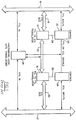
- a communications channel or communications bus 10 is part of a TTL system, not shown, to which are connected equipment, components or devices such as printers, mass storage devices and the like, having relatively slow data transfer rates.
- Another communications channel 12 is adapted for communications among higher performance components, such as computer processors that operate under the ECL electrical characteristics format or standard.
- Translator 14 is generally connected to communications bus 10 directly, although it is shown for clarity in the FIGURE as an electrical connection 16.
- an ECL to TTL translator 18 is connected directly to the ECL bus 12, but is shown in the FIGURE as electrically connected by means of lines 20.
- TTL control device 22 and ECL control device 24 Connected respectively to translators 14 and 18 are TTL control device 22 and ECL control device 24. Controllers 22 and 24 control the direction of the data path (i.e., from TTL side to ECL side or from ECL side to TTL side). Controllers 22 and 24 are connected to one another over lines 26 and are also connected directly and respectively to translators 14 and 18 over lines 28 and 30. Translators 14 and 18 are connected to one another internally in the chip by means of an electrical connection 32.
- a device 34 having logic for allowing storage and/or manipulation of data. Often data is transferred at a faster rate over the ECL communications channel 12 than it is over the TTL communications channel 10.
- logic device 34 is also connected to lines 26 between controllers 22 and 24 for the purpose of synchronizing disparate data flow rates therebetween.
- At least five components and a plurality of signal lines were required in the prior art to perform an interfacing function between communications buses 10 and 12.
- Data generated or transmitted by a device, not shown, connected to TTL communications bus 10 would be translated, stored or manipulated by the foregoing apparatus before being applied to a device, not shown, connected to ECL communications channel 12.
- FIGURE 2 there is shown an integrated circuit (IC) chip 50 in accordance with the present invention on which is located a plurality of bond pads 52 and 53.
- Bond pads 52 can be connected to one of the communications buses, not shown in this FIGURE.
- bond pads 53 can be connected to a second communications bus.
- data from the first communications bus is ported into the IC 50 by means of bond pads 52 and eventually is ported out to the second communications bus by means of bond pads 53.
- information initiated from the second communications bus can be ported into the IC 50 by means of bond pads 53 and applied to the first communications bus by means of bond pads 52.
- the gate array of the present invention integrates up to 410 ECL-equivalent gates to eliminate so-called "glue” logic. This results in reduced board space and improved reliability.
- the array is especially useful in systems that require ECL speeds with TTL compatability.
- a plurality of input/output (I/O) cells is identified by reference numeral 54.
- ten I/O cells form an interface between the first communications bus and a plurality of internal logic cells, hereinafter described.
- another ten I/O cells 56 are disposed adjacent bond pads 53 for cooperation with the second communications bus.
- I/O cells 54 and 56 Disposed between, the two banks of I/O cells 54 and 56 is a plurality of internal logic cells 58 arranged, in the preferred embodiment, in five banks of eight cells apiece, providing a total of 40 internal logic cells. This arrangement allows for the design of hard macros (multicell macros having fixed, predefined interconnect patterns) that are as large as eight cells long, filling an entire column.
- the I/O cells 54 and 56 are described in greater detail below, as are internal logic cells 58.
- FIGURE 2 Depicted in FIGURE 2 is the IC 50 configured in a so-called blank or uncustomized bus control gate array.
- This blank gate array can be customized according to specific requirements of a user by electrically connecting the bond pads 52 and 53 or any combination thereof to any one or more I/O cells 54 and 56 or any one or more internal logic cells 58, an example of which is described hereinbelow.
- Each internal logic cell 58 contains a fixed array of 19 transistors and 32 resistors that can be interconnected with a metal pattern to perform a wide variety of logic functions. These functions are known as macrocells. Functions as complex as a D flip flop can be implemented in one logic cell.
- a user having specific, predetermined requirements for transferring data from one communications bus to another communications bus or vice versa can configure his or her gate array IC 50 appropriately for that purpose.
- Parameters to be considered when configuring a gate array IC 50 include, but are not limited to:
- any configuration is possible within the limits of the number of bond pads 52 and 53, I/O cells 54 and 56 and internal logic cells 58 within one IC chip 50.
- Typical speed of the ECL gates is 280 ps, operating with typical power of 1.5 to 4.5 mW/gate. Power consumption depends on a number of factors: population of the array, specific macros used and programmable power/speed choices. A maximum of 1.5 Watts is available. Current switches are fixed and the Output Emitter Followers (OEFs) are programmable to low or medium options. Medium OEFs have greater speed than do low OEF's.
- OEFs Output Emitter Followers
- the gate array of the present invention can operate in four different modes of external logic levels: TTL, Pseudo ECL (PECL), True ECL (TECL), TTL & TECL, TTL & PECL.
- TTL mode ECL internal speeds are achieved while TTL I/O levels are supplied for interface with TTL systems.
- PECL mode a positive (+5 V) supply is used.
- TECL mode provides compatability with pure ECL systems.
- the TTL & TECL mode provides level translation capabilities for both TTL and True ECL, useful in mixed technology systems.
- TTL mode ECL internal circuits provide high performance in TTL-compatible systems.
- PECL mode reduces level translator delays between closely coupled blocks in a TTL environment.
- TTL & TECL mode provides level translation capabilities between TTL and True ECL functions.
- PECL & TTL provide translation between TTL and Psuedo ECL functions.
- FIGURE 3 there is shown an exploded view of a physical layout of a previously blank or uncustomized IC 50 that has been customized for a particular function.
- the customization of IC 50 is facilitated by individually programming the array mask by any suitable technique well known in the art.
- a plurality of lines connect individual internal logic cells 58 to one another, to selected I/O cells 54 and 56 and to selected bond pads 52 and 53.
- selected I/O cells 54 can be connected individually to one another as well as to selected bond pads 52 and 53 and, of course, to selected internal logic cells 58 and banks thereof.
- bond pads 52 and 53 can also be connected to one another.
- the configuration disclosed in FIGURE 3 represents a TTL/ECL bidirectional bus transceiver.
- ECL data is connected to bond pads ED0-ED7 at reference numeral 90.
- TTL data is connected to bond pads D0-D7 at reference numeral 92.
- the interconnection between the two aforementioned buses is by internal signal lines 94.
- Simple handshaking and control is facilitated by direction and enable pins 96.
- Internal logic to arbitrate data transfer is facilitated within the two internal cells and one I/O cell 98.
- the ECL output drivers are disposed in I/O cells 100.
- the TTL I/O translators are in I/O cells 102.
- An additional power pad for VCCO is shown at reference numeral 104.
- bias generation network is not shown in the FIGURES, although as a practical matter such bias generation network is normally required for a gate array with ECL capability.
- the bias generation network is used to provide reference levels for internal and external signals. The use of bias generation networks is well known in the art and need not be explained further here.
- FIGURE 4 there is shown a schematic diagram of a so-called blank internal logic cell 58 (FIGURE 2), in which no connections between components exist other than the hard wired device boundary connections.
- FIGURE 2 a schematic diagram of a so-called blank internal logic cell 58 (FIGURE 2), in which no connections between components exist other than the hard wired device boundary connections.
- nineteen transistors T1-T19 are shown generally disconnected, but can be connected to one another according to certain predetermined rules.
- resistors R1-R30 are shown connected to common contacts. They can be connected en say, however, to one another and to other components on the IC board 58.
- Each internal logic cell 58 can be customized (i.e., the components thereon can be connected to one another) according to certain predetermined desired functions and requirements. For example, if a particular internal logic cell 58 were to be configured as a D-latch with Reset circuit, the transistors and resistors are connected to one another in a predetermined, specified manner. Similarly, if an internal logic cell 58 were to function as a 2-to-1 inverting multiplexer, flip flop, gate or the like, the same transistors and resistors or other transistors and resistors would be connected to one another in a different manner in accordance with functions that such internal logic cell 58 were to perform.
- Each logic cell contains a 2-to-1 power selection system for the Output Emitter Follower (OEF).
- OEF controls output metal delays. This allows a trade-off between speed and power in critical paths at both the chip and system levels.
- Power supplies are connected to the internal logic cell 58 and are shown in this FIGURE as TTLVCC and TTLGND. Other power supplies, however, can be connected to the internal logic cell 58. A description of the power supplies is provided hereinbelow.
- the present invention can be used in several power modes to meet various applications.
- a 24-pin dual in-line package is suitable for the following power modes.
- ECLVCC is a positive power supply for the internal ECL circuitry. In TECL and ECL ONLY modes, it is 0 volts. In both PECL modes it is +5 volts.
- TTLVCC is a positive power supply for TTL compatible outputs. It is +5 volts in all modes with TTL outputs.
- VEE is a negative supply for the internal ECL circuitry. In both PECL modes it is 0 volts. In TECL and ECL ONLY modes it is -5.2 volts for 10K and -4.5 volts for 100K.
- VCCO is a supply that provides switching drive for ECL outputs. In TECL and ECL ONLY modes it is 0 volts and is physically connected internally to TTLGND. In both PECL modes it is +5 volts and is physically separate from TTLGND.
- TTLGND is a negative power supply that provides switching drive for TTL outputs. It is 0 volts in all modes that have TTL outputs. In TECL and ECL ONLY modes it is physically connected to VCCO. In both PECL modes it is physically separate from VCCO.
- FIGURE 5 there is shown a dual latch circuit configured from a blank input logic cell 58 (FIGURE 4).
- Other dual transistor configurations 2T7 and 2T8 form a basic logic gate 72.
- transistors 2T9 and 2T10 form another logic gate 74, the data input of which is shown as letter A.
- data input A is data input B for the second latch.
- a current mirror 76 comprises transistors 1T16-1T19. Current mirror 76 determines the amount of current used by the gates. Also shown in FIGURE 5 is a plurality of resistors (for example, 1R22-1R24, shown generally at reference numeral 78). The outputs of the latches are shown as reference letters YA and YB, respectively, in this FIGURE.
- the latch shown in FIGURE 5 is a typical latch known to those with ordinary skill in ECL technology and the gates are adapted for ECL operation.
- This internal logic cell 58 in ECL format can be found anywhere within the bank of internal logic cells 58 in the integrated circuit 50, due to the fact that TTL to ECL translators in I/O cells 54 and 56 (FIGURE 2) are used to convert TTL signals to ECL format.
- TTL to ECL translators in I/O cells 54 and 56 (FIGURE 2) are used to convert TTL signals to ECL format.
- all signals on the IC 50 downstream of the translators, not shown, are adapted for use with ECL.
- FIGURE 6 there is shown a schematic diagram of a blank I/O cell 54 (FIGURE 2), twenty of which reside on the array, and any of which can be used as input, output or bidirectional; true and complement outputs are available on-chip which eliminate inverter delays and reduce power and cell usage; 25 to 50 ohm ECL outputs are also available.
- the I/O cell 54 has transistors T1-T35 and resistors R1-R41.
- diodes D1-D6 are also part of the I/O cell 54 or 56. These components provide the capability of level shifting from internal ECL logic levels to various external signal levels. Any of the twenty I/O locations can be designated as input, output or bidirectional; TTL, TECL or PECL. Generally, ECL inputs are applied directly into the interface cells. However, I/O cells may be used as ECL inputs when necessary. There are no restrictions associating or confining specific I/O macrocells to specific I/O locations.
- power supplies are connected to the I/O cells 54 and 56 and are shown in this FIGURE as TTLVCC and TTLGND. Once again, other power supplies can be connected to the I/O cells 54.
- a description of the power supplies similar to the description provided above with regard to the internal logic cells (FIGURE 4), is provided hereinbelow.
- ECLVCC is a positive power supply for the internal ECL circuitry. In TECL and ECL ONLY modes, it is 0 volts. In both PECL modes it is +5 volts.
- TTLVCC is a positive power supply for TTL compatible outputs. It is +5 volts in all modes with TTL output.
- VEE is a negative supply for the internal ECL circuitry. In both PECL modes it is 0 volts. In TECL and ECL ONLY modes it is -5.2 volts for 10K and -4.5 volts for 100K.
- VCCO is a supply that provides switching drive for ECL outputs. In TECL and ECL ONLY modes it is 0 volts and is physically connected internally to TTLGND. In both PECL modes it is +5 volts and is physically separate from TTLGND.
- TTLGND is a negative power supply that provides switching drive for TTL outputs. It is 0 volts in all modes that have TTL outputs. In TECL and ECL ONLY modes it is physically connected to VCCO. In both PECL modes it is physically separate from VCCO.
- the I/O cells 54 and 56 can be customized by a user in order to fulfill specific requirements and functions. Sample functions that an I/O cell 54 and 56 can perform are: TTL to ECL translation; ECL to TTL translation; ECL input with ECL output; and TTL input with TTL output. I/O cells 54 and 56 can be programmed for I/O bus translation regardless of the bus protocol of either of the communications buses connected thereto.
- FIGURE 7 there is shown a schematic diagram of a customized I/O cell 54 or 56 (FIGURE 2), which is used to translate ECL formatted signals from an ECL communications, channel, not shown, to TTL formatted signals for use with a TTL communications channel, not shown.
- Output transistors are located adjacent the bond pads 52 (FIGURE 2).
- the ECL portion of I/O cell 54 is shown in phantom and identified as reference numeral 80.
- the remainder of I/O cell 54 shown in FIGURE 7 represents the TTL portion of the circuit.
- I/O cell 54 translates TECL formatted data to TTL formatted data
- I/O cells 54 for translating PECL formatted data to TTL formatted data
- complementary cells for translating in the reverse direction and other cells for handling different parameters such as three-state versus open collector devices, 8 milliamp versus 16 milliamp devices and the like.
- a separate I/O cell 54 is required for each translation possibility which, in turn, is dependent upon the aforementioned parameters.
- the drive requirement for external signals requires I/O cells to provide additional current drive for signals that are destined for off-chip destinations.
- I/O cells 54 and 58 may be required to convert internal ECL signals to external ECL signals, the latter usually having greater power requirements.
- the present invention residing on one IC chip 50 (FIGURE 2), is a direct replacement for the plurality of components commonly used in the prior art (FIGURE 1) and that such a replacement and substitution represents improved characteristics and a significant advance in the art in terms of power consumption, speed, geographical displacement, reduced parts inventory and cost.
Landscapes
- Engineering & Computer Science (AREA)
- Computer Hardware Design (AREA)
- General Engineering & Computer Science (AREA)
- Physics & Mathematics (AREA)
- Computing Systems (AREA)
- Mathematical Physics (AREA)
- Theoretical Computer Science (AREA)
- General Physics & Mathematics (AREA)
- Design And Manufacture Of Integrated Circuits (AREA)
- Logic Circuits (AREA)
- Paper (AREA)
- Electrotherapy Devices (AREA)
- Bus Control (AREA)
- Small-Scale Networks (AREA)
- Semiconductor Integrated Circuits (AREA)
Claims (10)
- Système pour raccorder deux canaux disparates de télécommunication numérique, ce système traduisant des signaux électriques passant entre les deux canaux (10, 12) d'une première logique associée au premier des canaux vers une seconde logique associée au second canal, caractérisé en ce qu'il comprend un circuit intégré (50) possédant une matrice de portes programmable par masquage des portes logiques (58) et un premier et un second moyen de raccordement à la demande entrée/sortie (54,56) respectivement connecté entre la matrice de portes logiques et les premier et second canaux de communication (10,12).
- Système selon la revendication 1, caractérisé en ce que les deux canaux de communication comprennent respectivement un premier bus (10) et un second bus (12).
- Système selon la revendication 1 ou la revendication 2 dans lequel la première logique est à transistor multiémetteur.
- Système selon l'une quelconque des revendications 1 à 3 dans lequel la seconde logique est à liaison par les émetteurs.
- Système selon l'une quelconque des revendications précédentes dans lequel les premier et second moyens de raccordement entrée/sortie (54, 56) sont aussi programmés par masquage.
- Système selon la revendication 4 dans lequel la logique à liaison par émetteurs est compatible à 10KHz.
- Système selon la revendication 4 dans lequel ladite logique à liaison par émetteurs est compatibles à 100KHz.
- Système selon l'une quelconque des revendications précédentes dans lequel la matrice de portes logiques (58) régule la performance électrique de chacun des moyens de raccordement entrée/sortie (54, 56).
- Système selon la revendication 8 dans lequel la matrice de portes logiques (58) régule en outre la direction et la cadence du flux d'informations entre les canaux de communication.
- Système selon la revendication 9 dans lequel la matrice de portes logiques (58) comprend en outre un moyen de stockage pour retenir temporairement l'information fournie par l'un des canaux de communication.
Applications Claiming Priority (2)
| Application Number | Priority Date | Filing Date | Title |
|---|---|---|---|
| US254751 | 1988-10-07 | ||
| US07/254,751 US4987578A (en) | 1988-10-07 | 1988-10-07 | Mask programmable bus control gate array |
Publications (3)
| Publication Number | Publication Date |
|---|---|
| EP0363086A2 EP0363086A2 (fr) | 1990-04-11 |
| EP0363086A3 EP0363086A3 (fr) | 1991-07-31 |
| EP0363086B1 true EP0363086B1 (fr) | 1996-06-12 |
Family
ID=22965459
Family Applications (1)
| Application Number | Title | Priority Date | Filing Date |
|---|---|---|---|
| EP89309931A Expired - Lifetime EP0363086B1 (fr) | 1988-10-07 | 1989-09-29 | Réseau de portes programmable au moyen d'un masque pour commande de bus |
Country Status (7)
| Country | Link |
|---|---|
| US (1) | US4987578A (fr) |
| EP (1) | EP0363086B1 (fr) |
| JP (1) | JPH02144650A (fr) |
| AT (1) | ATE139356T1 (fr) |
| DE (1) | DE68926649T2 (fr) |
| ES (1) | ES2087867T3 (fr) |
| GR (1) | GR3020218T3 (fr) |
Families Citing this family (12)
| Publication number | Priority date | Publication date | Assignee | Title |
|---|---|---|---|---|
| JPH03109767A (ja) * | 1989-09-25 | 1991-05-09 | Nec Corp | 半導体集積回路装置 |
| WO1991011870A1 (fr) * | 1990-02-02 | 1991-08-08 | Codex Corporation | Adaptateur d'interfaces |
| US5347181A (en) * | 1992-04-29 | 1994-09-13 | Motorola, Inc. | Interface control logic for embedding a microprocessor in a gate array |
| GB9209394D0 (en) * | 1992-04-30 | 1992-06-17 | Mini Agriculture & Fisheries | Data storage tags |
| US5691218A (en) * | 1993-07-01 | 1997-11-25 | Lsi Logic Corporation | Method of fabricating a programmable polysilicon gate array base cell structure |
| US5552333A (en) * | 1994-09-16 | 1996-09-03 | Lsi Logic Corporation | Method for designing low profile variable width input/output cells |
| US5758132A (en) * | 1995-03-29 | 1998-05-26 | Telefonaktiebolaget Lm Ericsson | Clock control system and method using circuitry operating at lower clock frequency for selecting and synchronizing the switching of higher frequency clock signals |
| US5970255A (en) * | 1995-10-16 | 1999-10-19 | Altera Corporation | System for coupling programmable logic device to external circuitry which selects a logic standard and uses buffers to modify output and input signals accordingly |
| US5760428A (en) * | 1996-01-25 | 1998-06-02 | Lsi Logic Corporation | Variable width low profile gate array input/output architecture |
| US5698873A (en) * | 1996-03-08 | 1997-12-16 | Lsi Logic Corporation | High density gate array base cell architecture |
| US6137340A (en) * | 1998-08-11 | 2000-10-24 | Fairchild Semiconductor Corp | Low voltage, high speed multiplexer |
| US7299203B1 (en) * | 2001-04-19 | 2007-11-20 | Xilinx, Inc. | Method for storing and shipping programmable ASSP devices |
Family Cites Families (8)
| Publication number | Priority date | Publication date | Assignee | Title |
|---|---|---|---|---|
| JPS57211248A (en) * | 1981-06-22 | 1982-12-25 | Hitachi Ltd | Semiconductor integrated circuit device |
| US4430582A (en) * | 1981-11-16 | 1984-02-07 | National Semiconductor Corporation | Fast CMOS buffer for TTL input levels |
| US4734592A (en) * | 1983-10-31 | 1988-03-29 | Texas Instruments Incorporated | Interface circuit for data processing system |
| US4614882A (en) * | 1983-11-22 | 1986-09-30 | Digital Equipment Corporation | Bus transceiver including compensation circuit for variations in electrical characteristics of components |
| EP0203700A3 (fr) * | 1985-04-19 | 1987-09-23 | Advanced Micro Devices, Inc. | Convertisseur de niveau logique |
| US4645954A (en) * | 1985-10-21 | 1987-02-24 | International Business Machines Corp. | ECL to FET interface circuit for field effect transistor arrays |
| US4719372A (en) * | 1986-02-03 | 1988-01-12 | International Business Machines Corporation | Multiplying interface circuit for level shifting between FET and TTL levels |
| FR2598871B1 (fr) * | 1986-05-14 | 1988-09-30 | Bendix Electronics Sa | Circuit d'interface bidirectionnel presentant un acces unipolaire et un acces bipolaire pour des signaux logiques |
-
1988
- 1988-10-07 US US07/254,751 patent/US4987578A/en not_active Expired - Lifetime
-
1989
- 1989-09-29 AT AT89309931T patent/ATE139356T1/de not_active IP Right Cessation
- 1989-09-29 ES ES89309931T patent/ES2087867T3/es not_active Expired - Lifetime
- 1989-09-29 DE DE68926649T patent/DE68926649T2/de not_active Expired - Fee Related
- 1989-09-29 EP EP89309931A patent/EP0363086B1/fr not_active Expired - Lifetime
- 1989-10-06 JP JP1262845A patent/JPH02144650A/ja active Pending
-
1996
- 1996-06-13 GR GR960401340T patent/GR3020218T3/el unknown
Also Published As
| Publication number | Publication date |
|---|---|
| GR3020218T3 (en) | 1996-09-30 |
| EP0363086A3 (fr) | 1991-07-31 |
| DE68926649D1 (de) | 1996-07-18 |
| US4987578A (en) | 1991-01-22 |
| ES2087867T3 (es) | 1996-08-01 |
| JPH02144650A (ja) | 1990-06-04 |
| DE68926649T2 (de) | 1997-01-02 |
| ATE139356T1 (de) | 1996-06-15 |
| EP0363086A2 (fr) | 1990-04-11 |
Similar Documents
| Publication | Publication Date | Title |
|---|---|---|
| US10700046B2 (en) | Multi-chip hybrid system-in-package for providing interoperability and other enhanced features to high complexity integrated circuits | |
| EP0363086B1 (fr) | Réseau de portes programmable au moyen d'un masque pour commande de bus | |
| EP0225715B1 (fr) | Cellule d'entrées/sorties programmable | |
| US6480025B1 (en) | Driver circuitry for programmable logic devices with hierarchical interconnection resources | |
| US6504399B2 (en) | Method and apparatus for universal program controlled bus architecture | |
| US5894228A (en) | Tristate structures for programmable logic devices | |
| US6472904B2 (en) | Double data rate input and output in a programmable logic device | |
| US7382156B2 (en) | Method and apparatus for universal program controlled bus architecture | |
| US5602494A (en) | Bi-directional programmable I/O cell | |
| US6239612B1 (en) | Programmable I/O cells with multiple drivers | |
| WO2002017081A1 (fr) | Procede et appareil permettant de combiner des architectures avec une option logique | |
| US4894563A (en) | Output macrocell for programmable logic device | |
| EP0448624B1 (fr) | Unitde de commande d'interface de bus pour systeme graphique d'ordinateur | |
| US5760719A (en) | Programmable I/O cell with data conversion capability | |
| US5869982A (en) | Programmable I/O cell with data conversion capability | |
| JPH02161820A (ja) | プログラマブル入出力回路及びプログラマブル論理素子 | |
| EP0897629B1 (fr) | Terminaison de ligne integree et commutable | |
| US5917337A (en) | Programmable I/O cell with data conversion capability | |
| KR100462437B1 (ko) | 선로수신기회로 | |
| Wirth | Bus Systems | |
| HK1017536B (en) | Integrated and switchable line termination | |
| CN87100464A (zh) | 多路异步通讯接口 | |
| WO1999059088A2 (fr) | Unite logique programmable munie d'une macrocellule controlee par un reseau logique programmable | |
| JP2006114116A (ja) | 半導体記憶装置の入出力回路、入出力方法、組立方法、及び半導体記憶装置 | |
| JPH0456514A (ja) | 半導体集積回路 |
Legal Events
| Date | Code | Title | Description |
|---|---|---|---|
| PUAI | Public reference made under article 153(3) epc to a published international application that has entered the european phase |
Free format text: ORIGINAL CODE: 0009012 |
|
| AK | Designated contracting states |
Kind code of ref document: A2 Designated state(s): AT BE CH DE ES FR GB GR IT LI LU NL SE |
|
| PUAL | Search report despatched |
Free format text: ORIGINAL CODE: 0009013 |
|
| AK | Designated contracting states |
Kind code of ref document: A3 Designated state(s): AT BE CH DE ES FR GB GR IT LI LU NL SE |
|
| 17P | Request for examination filed |
Effective date: 19920109 |
|
| 17Q | First examination report despatched |
Effective date: 19940405 |
|
| GRAH | Despatch of communication of intention to grant a patent |
Free format text: ORIGINAL CODE: EPIDOS IGRA |
|
| GRAA | (expected) grant |
Free format text: ORIGINAL CODE: 0009210 |
|
| AK | Designated contracting states |
Kind code of ref document: B1 Designated state(s): AT BE CH DE ES FR GB GR IT LI LU NL SE |
|
| REF | Corresponds to: |
Ref document number: 139356 Country of ref document: AT Date of ref document: 19960615 Kind code of ref document: T |
|
| REG | Reference to a national code |
Ref country code: ES Ref legal event code: BA2A Ref document number: 2087867 Country of ref document: ES Kind code of ref document: T3 |
|
| REF | Corresponds to: |
Ref document number: 68926649 Country of ref document: DE Date of ref document: 19960718 |
|
| ET | Fr: translation filed | ||
| REG | Reference to a national code |
Ref country code: ES Ref legal event code: FG2A Ref document number: 2087867 Country of ref document: ES Kind code of ref document: T3 |
|
| PGFP | Annual fee paid to national office [announced via postgrant information from national office to epo] |
Ref country code: FR Payment date: 19960808 Year of fee payment: 8 |
|
| ITF | It: translation for a ep patent filed | ||
| REG | Reference to a national code |
Ref country code: GR Ref legal event code: FG4A Free format text: 3020218 |
|
| PLBE | No opposition filed within time limit |
Free format text: ORIGINAL CODE: 0009261 |
|
| STAA | Information on the status of an ep patent application or granted ep patent |
Free format text: STATUS: NO OPPOSITION FILED WITHIN TIME LIMIT |
|
| 26N | No opposition filed | ||
| PGFP | Annual fee paid to national office [announced via postgrant information from national office to epo] |
Ref country code: GR Payment date: 19970725 Year of fee payment: 9 |
|
| PGFP | Annual fee paid to national office [announced via postgrant information from national office to epo] |
Ref country code: SE Payment date: 19970818 Year of fee payment: 9 |
|
| PGFP | Annual fee paid to national office [announced via postgrant information from national office to epo] |
Ref country code: AT Payment date: 19970821 Year of fee payment: 9 |
|
| PGFP | Annual fee paid to national office [announced via postgrant information from national office to epo] |
Ref country code: LU Payment date: 19970911 Year of fee payment: 9 |
|
| PG25 | Lapsed in a contracting state [announced via postgrant information from national office to epo] |
Ref country code: FR Free format text: THE PATENT HAS BEEN ANNULLED BY A DECISION OF A NATIONAL AUTHORITY Effective date: 19970930 |
|
| PGFP | Annual fee paid to national office [announced via postgrant information from national office to epo] |
Ref country code: BE Payment date: 19971007 Year of fee payment: 9 |
|
| PGFP | Annual fee paid to national office [announced via postgrant information from national office to epo] |
Ref country code: CH Payment date: 19971014 Year of fee payment: 9 |
|
| REG | Reference to a national code |
Ref country code: FR Ref legal event code: ST |
|
| PG25 | Lapsed in a contracting state [announced via postgrant information from national office to epo] |
Ref country code: LU Free format text: LAPSE BECAUSE OF NON-PAYMENT OF DUE FEES Effective date: 19980929 Ref country code: AT Free format text: LAPSE BECAUSE OF NON-PAYMENT OF DUE FEES Effective date: 19980929 |
|
| PG25 | Lapsed in a contracting state [announced via postgrant information from national office to epo] |
Ref country code: SE Free format text: LAPSE BECAUSE OF NON-PAYMENT OF DUE FEES Effective date: 19980930 Ref country code: LI Free format text: LAPSE BECAUSE OF NON-PAYMENT OF DUE FEES Effective date: 19980930 Ref country code: GR Free format text: LAPSE BECAUSE OF NON-PAYMENT OF DUE FEES Effective date: 19980930 Ref country code: CH Free format text: LAPSE BECAUSE OF NON-PAYMENT OF DUE FEES Effective date: 19980930 Ref country code: BE Free format text: LAPSE BECAUSE OF NON-PAYMENT OF DUE FEES Effective date: 19980930 |
|
| BERE | Be: lapsed |
Owner name: ADVANCED MICRO DEVICES INC. Effective date: 19980930 |
|
| REG | Reference to a national code |
Ref country code: CH Ref legal event code: PL |
|
| EUG | Se: european patent has lapsed |
Ref document number: 89309931.7 |
|
| REG | Reference to a national code |
Ref country code: GB Ref legal event code: IF02 |
|
| PGFP | Annual fee paid to national office [announced via postgrant information from national office to epo] |
Ref country code: NL Payment date: 20020618 Year of fee payment: 14 |
|
| PGFP | Annual fee paid to national office [announced via postgrant information from national office to epo] |
Ref country code: GB Payment date: 20020808 Year of fee payment: 14 |
|
| PGFP | Annual fee paid to national office [announced via postgrant information from national office to epo] |
Ref country code: ES Payment date: 20020924 Year of fee payment: 14 |
|
| PGFP | Annual fee paid to national office [announced via postgrant information from national office to epo] |
Ref country code: DE Payment date: 20020930 Year of fee payment: 14 |
|
| PG25 | Lapsed in a contracting state [announced via postgrant information from national office to epo] |
Ref country code: GB Free format text: LAPSE BECAUSE OF NON-PAYMENT OF DUE FEES Effective date: 20030929 |
|
| PG25 | Lapsed in a contracting state [announced via postgrant information from national office to epo] |
Ref country code: ES Free format text: LAPSE BECAUSE OF NON-PAYMENT OF DUE FEES Effective date: 20030930 |
|
| PG25 | Lapsed in a contracting state [announced via postgrant information from national office to epo] |
Ref country code: NL Free format text: LAPSE BECAUSE OF NON-PAYMENT OF DUE FEES Effective date: 20040401 Ref country code: DE Free format text: LAPSE BECAUSE OF NON-PAYMENT OF DUE FEES Effective date: 20040401 |
|
| GBPC | Gb: european patent ceased through non-payment of renewal fee |
Effective date: 20030929 |
|
| NLV4 | Nl: lapsed or anulled due to non-payment of the annual fee |
Effective date: 20040401 |
|
| REG | Reference to a national code |
Ref country code: ES Ref legal event code: FD2A Effective date: 20030930 |
|
| PG25 | Lapsed in a contracting state [announced via postgrant information from national office to epo] |
Ref country code: IT Free format text: LAPSE BECAUSE OF NON-PAYMENT OF DUE FEES;WARNING: LAPSES OF ITALIAN PATENTS WITH EFFECTIVE DATE BEFORE 2007 MAY HAVE OCCURRED AT ANY TIME BEFORE 2007. THE CORRECT EFFECTIVE DATE MAY BE DIFFERENT FROM THE ONE RECORDED. Effective date: 20050929 |