EP0363231A1 - Verfahren zur Übertragung von Nachrichten mittels einer bidirektionalen Strecke, und Gerät zu dessen Durchführung - Google Patents
Verfahren zur Übertragung von Nachrichten mittels einer bidirektionalen Strecke, und Gerät zu dessen Durchführung Download PDFInfo
- Publication number
- EP0363231A1 EP0363231A1 EP19890402244 EP89402244A EP0363231A1 EP 0363231 A1 EP0363231 A1 EP 0363231A1 EP 19890402244 EP19890402244 EP 19890402244 EP 89402244 A EP89402244 A EP 89402244A EP 0363231 A1 EP0363231 A1 EP 0363231A1
- Authority
- EP
- European Patent Office
- Prior art keywords
- station
- clock
- flip
- transmission
- central station
- Prior art date
- Legal status (The legal status is an assumption and is not a legal conclusion. Google has not performed a legal analysis and makes no representation as to the accuracy of the status listed.)
- Granted
Links
Images

Classifications
-
- H—ELECTRICITY
- H04—ELECTRIC COMMUNICATION TECHNIQUE
- H04L—TRANSMISSION OF DIGITAL INFORMATION, e.g. TELEGRAPHIC COMMUNICATION
- H04L5/00—Arrangements affording multiple use of the transmission path
- H04L5/14—Two-way operation using the same type of signal, i.e. duplex
- H04L5/1423—Two-way operation using the same type of signal, i.e. duplex for simultaneous baseband signals
-
- H—ELECTRICITY
- H04—ELECTRIC COMMUNICATION TECHNIQUE
- H04L—TRANSMISSION OF DIGITAL INFORMATION, e.g. TELEGRAPHIC COMMUNICATION
- H04L7/00—Arrangements for synchronising receiver with transmitter
- H04L7/0008—Synchronisation information channels, e.g. clock distribution lines
Definitions
- the present invention relates to a method of transmitting information in the form of electrical signals over a bidirectional link used in particular for the exchange of data between the central organs and the peripheral organs of a computer system.
- one or more peripheral stations are linked to a central station by one or more bidirectional transmission channels.
- an information signal received must be present on the one hand for a minimum time to be validated by the active edge of a clock signal (called pre-display time or “set up time” tsu) before the arrival of this active front, and on the other hand for another minimum time (called hold time or “hold time” th) after the arrival of this same active front.
- active edge is meant a transition between two electrical voltages, from a high state to a low state (falling edge) or the reverse (rising edge).
- the times tsu and th depend on the technology used for manufacturing the electronic components, and on the specific circuits implemented in the stations when information is received. These times are of the order of 10-15 ns for tsu and 0-5 ns for th in the case of a rocker / tri-state carrier sub-assembly using a so-called fast technology (“FAST”) .
- FAST fast technology
- a synchronous transmission which uses a synchronization clock sent by the central station, is carried out either in single-phase mode (the circuits of the Transmitter and Receiver stations are then synchronized on the same rising [or falling] edge of the clock signal. ) or in two-phase mode (The circuits of the Transmitter and Receiver stations are then synchronized on different rising and falling edges of the clock signal).
- bidirectional links require resynchronization from the local clock of the receiver via a circuit called a unifier which, in addition to the increase in the number of components (use of two clocks and unifying circuit), also introduces a delay. It is customary to consider that the increase in flow occurs always balance by a delay in the routing of information (speed favored at the expense of transmission time).
- the invention provides a method of transmitting information in the form of electrical signals over a bidirectional link comprising a central station and a peripheral station connected to the central station by a bidirectional transmission channel, said central station being provided with a clock delivering a synchronization signal to said peripheral station, the method being characterized in that synchronization is carried out, on the one hand in biphase mode during transmission from the central station, on the other hand by single-phase mode when transmitting from the peripheral station.
- the peripheral station is synchronized to the transmission and to the reception on the same edge of the clock signal.
- the central station transmits on the falling edge of the clock signal and receives on the rising edge of said signal.
- the invention also relates to a device for implementing the method according to the invention of the type comprising a central station, a peripheral station connected to the central station by a bidirectional transmission channel, said central station being provided with a clock delivering a synchronization signal to said peripheral station via a clock signal transmission line, said device being characterized in that it furthermore comprises means allowing synchronization on the one hand in biphase mode during broadcasts from the station on the other hand in single-phase mode when transmitting from the peripheral station.
- the device comprises at least one elementary circuit provided with transmission / reception flip-flops, disposed in the central station and connected by a bidirectional transmission line to another elementary circuit provided with transmission / reception flip-flops reception and disposed in the peripheral station, said flip-flops having the same triggering characteristics from an input H capable of receiving a clock signal generated by means of said clock, said device being characterized in that said means of synchronization include an inverter gate arranged between the clock output and the input H of one of the two flip-flops constituted by the transmission flip-flop of the central station and the reception flip-flop of the peripheral station, the input H of the other of said two flip-flops being attacked by the clock output signal, the inputs H of flip-flops receiving from the central station and sending from the peripheral station being attacked by the same signal generated from the clock.
- said means of synchronization include an inverter gate arranged between the clock output and the input H of one of the two flip-flops constituted by the transmission flip-flop of the central station and the reception flip-flop of the peripheral station
- the device for implementing the invention presented below shows a simple structure with few complementary components and therefore inexpensive.
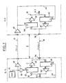
- the bidirectional link consists of a central station SC connected to a peripheral station SP by a bidirectional channel 10.
- This bidirectional channel 10 of length 1 is constituted for example by a parallel transmission channel of width 1 byte.
- Each line of the parallel channel carries a signal / XADi / where i is an integer between 0 and 7.
- the width of the channel can be increased to 16 or 32 bits and even to -of the.
- the bidirectional link is used for example in a computer system to convey information, in the form of electrical signals, such as data and / or addresses, from a central subsystem to a peripheral subsystem.
- the various subsystems are neither shown nor described, with the exception of their transmission stations SC and SP.
- a unidirectional clock signal transmission line, line 12 capable of delivering to the station SP a clock signal / XCL / generated by a transmission synchronization clock 14 belonging to the station SC.
- FAST rapid technology
- the central station SC comprises, in addition to the clock 14, a separator-amplifier 16 of the F245 type working in transmission mounted between the clock 14 and the clock line 12, and a circuit of the 29F52 type consisting of 8 elementary circuits 18 (one bit circuit to be transmitted).
- Each of the elementary circuits 18 includes storage flip-flops 20, 26 mounted two by two in parallel to work one on transmission (flip-flop 20) and the other on reception (flip-flop 26). If we consider Figure 1 where only an elementary circuit 18 is represented, we can notice the transmission flip-flop 20 of type D with its data input E1 connected to one of the lines BC of an internal bidirectional bus of the central subsystem and its data output S1 connected through a three-state gate 22 to junction 24 located at the end SC side of line i of channel 10.
- the receiving flip-flop 26 also of the type D, is mounted in parallel with the flip-flop 20, with its input E0 connected to junction 24, its output S0 connected through a three-state carrier 28 to the line BC.
- the clock input H0 of the reception flip-flop 26 is connected directly to the output of the clock 14 by line 29 while the clock input H1 of the transmission flip-flop 20 is connected to the output of the clock 14 through a type F reversing door 30 04.
- the reception flip-flop 34 has its data input E2 connected to the junction 36 located at the side end SP of line i of channel 10 and its data output S2 connected through a three-state carrier 38 to a line BP of an internal bidirectional bus of the peripheral subsystem.
- the transmission flip-flop 40 has its input E3 connected to the bus BP and its output S3 connected to the junction 36 through a three-state gate 42.
- the clock inputs H2 and H3 flip-flops 34 and 40 are directly connected by a line 44 to the output of a separator-amplifier 46 of the F245 type, the input of which is connected to the clock line 12 to receive the signal / XCL / from the clock 14 .
- the clock signal / XCL / has two essential parameters, its frequency and its duty cycle (ie the ratio of the pulse duration to the total period T of the signal). The choice of these parameters depends on the technology used and the construction characteristics of the circuits, in this case the length 1 of the bidirectional link defined between the two junctions 24 and 36 of track 10.
- the duty cycle of the signal clock is chosen in the form 1 / N where N is an integer, preferably 1/3 with "FAST" technology.
- line 10 is then conditioned in this direction of transmission by sending control signals to the validation inputs of the three-state gates 28 and 42
- the outputs of these doors are said to be disconnected by placing these same doors in a high impedance state.
- the gates 22 and 38 are kept in the low impedance state allowing them to deliver the input signal at their output.
- the signal / XADi / then passes over the corresponding line i of channel 10 to attack the input E2 of the reception flip-flop 34 itself triggered by the rising edge of the clock signal at its input H2.
- This data signal passes through the three-state gate 38 to appear on the corresponding line of the BP bus. It should be noted that thanks to the presence of the inverter 30, the transmission was carried out synchronously in biphase mode. .
- the device In the event of data transmission from the peripheral station to the central station, the device operates in a similar manner with inversion of the states high / low impedance of three-state gates. However, the transmission is carried out synchronously in single-phase mode.
- the timing diagram of Figure 2 illustrates the advantages provided by the invention.
- the left part of Figure 2 illustrates a data transmission in biphase mode from the central station SC to the peripheral station SP while the right part of Figure 2 illustrates a data transmission in single-phase mode from the peripheral station SP to the station central SC
- the timing diagram represents the clock signals / XCL / and data / XADi / at each end SC and SP of the bidirectional link.
- the clock signal / XCL / of period T has a general rectangular shape with a duty cycle of 1/3.
- this signal appears with its rising edges MC0, MC1, MCn and its falling edges DC0, DC1, ... DCn.
- the clock signal appears shifted in time by a duration dc and appears with its rising edges MP0, MP1, ... MPn and its falling edges DP0, DP1, ... DPn.
- the data signals / XADi / are synchronized by the clock 14, either from a falling edge DC from / XCL / (transmission from SC to SP) or from a rising edge MP from / XCL / (l 'transmission from SP to SC).
- the cycle has a duration equal to a clock period T.
- the duration of validity of the data signal is equal to a period T (the transmission flip-flops are triggered at each active edge of the clock signal).
- the data signal appears offset in time by a duration da and disappears offset by a duration db.
- condition (3) imposes a limitation on dc + da which is therefore linked at length 1 of the bidirectional link.
- condition (3) links the performance of the link to its length.
- the lower limit of T is reduced to twice the transmission time in the link lines.
- the transmission method according to the invention and its implementation device make it possible to significantly increase the performance of bidirectional links with a reduced number of additional components, without however requiring resynchronization from the local clock of the Receiver station.
- the method according to the invention can be used in various types of synchronous transmission, serial or parallel, in particular in message mode, without particular adaptation difficulty.
Landscapes
- Engineering & Computer Science (AREA)
- Signal Processing (AREA)
- Computer Networks & Wireless Communication (AREA)
- Bidirectional Digital Transmission (AREA)
- Synchronisation In Digital Transmission Systems (AREA)
- Small-Scale Networks (AREA)
- Communication Control (AREA)
Applications Claiming Priority (2)
| Application Number | Priority Date | Filing Date | Title |
|---|---|---|---|
| FR8811389A FR2635933B1 (fr) | 1988-08-31 | 1988-08-31 | Procede de transmission d'information sur une liaison bidirectionnelle et dispositif de mise en oeuvre de ce procede |
| FR8811389 | 1988-08-31 |
Publications (2)
| Publication Number | Publication Date |
|---|---|
| EP0363231A1 true EP0363231A1 (de) | 1990-04-11 |
| EP0363231B1 EP0363231B1 (de) | 1993-10-27 |
Family
ID=9369611
Family Applications (1)
| Application Number | Title | Priority Date | Filing Date |
|---|---|---|---|
| EP89402244A Expired - Lifetime EP0363231B1 (de) | 1988-08-31 | 1989-08-09 | Verfahren zur Übertragung von Nachrichten mittels einer bidirektionalen Strecke, und Gerät zu dessen Durchführung |
Country Status (6)
| Country | Link |
|---|---|
| US (1) | US5048061A (de) |
| EP (1) | EP0363231B1 (de) |
| JP (1) | JPH0795738B2 (de) |
| DE (1) | DE68910265T2 (de) |
| ES (1) | ES2047692T3 (de) |
| FR (1) | FR2635933B1 (de) |
Families Citing this family (4)
| Publication number | Priority date | Publication date | Assignee | Title |
|---|---|---|---|---|
| US5864592A (en) * | 1992-11-03 | 1999-01-26 | Pairgain Technologies, Inc. | Timing recovery system for digital subscriber line transceivers |
| KR20000027466A (ko) * | 1998-10-28 | 2000-05-15 | 구자홍 | 양방향 통신 장치 |
| FI19992230A7 (fi) * | 1999-10-15 | 2001-04-16 | James Casserly | Ilmoitusten toimitusmekanismi |
| US6772251B1 (en) * | 2001-05-04 | 2004-08-03 | Cypress Semiconductor Corporation | Bit interleaved data serial interface |
Citations (1)
| Publication number | Priority date | Publication date | Assignee | Title |
|---|---|---|---|---|
| CH646826A5 (en) * | 1979-10-15 | 1984-12-14 | Siemens Ag Albis | Data transmission method |
Family Cites Families (9)
| Publication number | Priority date | Publication date | Assignee | Title |
|---|---|---|---|---|
| JPS5451340A (en) * | 1977-09-29 | 1979-04-23 | Mitsubishi Electric Corp | Data transmitter |
| US4375103A (en) * | 1980-09-17 | 1983-02-22 | International Business Machines Corp. | Method and apparatus of signalling request to send clear to send delay |
| US4475191A (en) * | 1982-12-10 | 1984-10-02 | At&T Bell Laboratories | Distributed time division multiplexing bus |
| GB8322992D0 (en) * | 1983-08-26 | 1983-09-28 | Gen Electric Co Plc | Line transmission systems |
| JPS60130235A (ja) * | 1983-12-16 | 1985-07-11 | Fujitsu Ltd | デ−タ・音声伝送装置 |
| US4757521A (en) * | 1984-05-17 | 1988-07-12 | Tie/Communications, Inc. | Synchronization method and apparatus for a telephone switching system |
| US4637016A (en) * | 1985-05-09 | 1987-01-13 | Northern Telecom Limited | Frame synchronization circuit for digital transmission system |
| JPS62168415A (ja) * | 1986-01-20 | 1987-07-24 | Fujitsu Ltd | ラツチ間伝送方式 |
| DE3751608T2 (de) * | 1986-09-01 | 1996-06-27 | Nippon Electric Co | Serielles Busschnittstellensystem zur Datenübertragung mit einer Zweidrahtleitung als Taktbus und Datenbus. |
-
1988
- 1988-08-31 FR FR8811389A patent/FR2635933B1/fr not_active Expired - Lifetime
-
1989
- 1989-08-09 ES ES89402244T patent/ES2047692T3/es not_active Expired - Lifetime
- 1989-08-09 DE DE89402244T patent/DE68910265T2/de not_active Expired - Fee Related
- 1989-08-09 EP EP89402244A patent/EP0363231B1/de not_active Expired - Lifetime
- 1989-08-29 US US07/400,136 patent/US5048061A/en not_active Expired - Lifetime
- 1989-08-30 JP JP22432289A patent/JPH0795738B2/ja not_active Expired - Fee Related
Patent Citations (1)
| Publication number | Priority date | Publication date | Assignee | Title |
|---|---|---|---|---|
| CH646826A5 (en) * | 1979-10-15 | 1984-12-14 | Siemens Ag Albis | Data transmission method |
Non-Patent Citations (2)
| Title |
|---|
| PATENT ABSTRACTS OF JAPAN, vol. 12, no. 7 (E-571)[2854], 9 janvier 1988; & JP-A-62 168 415 (FUJITSU LTD.) 24.07.1987 * |
| PATENT ABSTRACTS OF JAPAN, vol. 3, no. 71 (E-118), 20 juin 1979; & JP-A-54 51 340 (MITSUBISHI DENKI K.K.) 23.04.1979 * |
Also Published As
| Publication number | Publication date |
|---|---|
| FR2635933A1 (fr) | 1990-03-02 |
| JPH02262739A (ja) | 1990-10-25 |
| DE68910265T2 (de) | 1994-03-03 |
| DE68910265D1 (de) | 1993-12-02 |
| US5048061A (en) | 1991-09-10 |
| EP0363231B1 (de) | 1993-10-27 |
| ES2047692T3 (es) | 1994-03-01 |
| JPH0795738B2 (ja) | 1995-10-11 |
| FR2635933B1 (fr) | 1990-10-12 |
Similar Documents
| Publication | Publication Date | Title |
|---|---|---|
| EP0108028B1 (de) | System zur Synchronisation digitaler Paketmultiplexe | |
| EP0407279B1 (de) | Kommunikationsnetz zwischen Teilnehmereinrichtungen | |
| EP0187067B1 (de) | Umschaltungssystem für ein digitales Übertragungsnetz | |
| WO1985001849A1 (fr) | Systeme de multiplexage numerique temporel asynchrone a bus distribue | |
| EP0621703B1 (de) | Verfahren und Vorrichtung zur Taktrückgewinnung und Synchronisierung für den Empfang über ein ATM-Netz übertragener Daten | |
| EP0108692B1 (de) | Verfahren und Einrichtung zur Übertragung von digitalen Daten | |
| EP0363231B1 (de) | Verfahren zur Übertragung von Nachrichten mittels einer bidirektionalen Strecke, und Gerät zu dessen Durchführung | |
| EP0120172B1 (de) | Businterfacevorrichtung für ein Datenverarbeitungssystem | |
| EP0340841B1 (de) | Koppelpunktschaltungselement zwischen zwei Daten-Sammelleitungen | |
| EP1004079B1 (de) | Verfahren und vorrichtung zur rückgewinnung von zeitverschobenen daten auf einem parallelen bus | |
| CA2046242C (fr) | Dispositif d'echantillonnage de donnees et systeme de transmission numerique de donnees en resultant | |
| EP0253281A1 (de) | Verfahren und Anordnung zur Phaseneinstellung digitalsynchroner Datenflüsse | |
| EP0056748B1 (de) | Verfahren zur empfangsseitigen Synchronisation paketweise übertragener, digitaler Signale | |
| FR2661578A1 (fr) | Dispositif de commutation dynamique pour le masquage d'erreurs dans un systeme a doublement du conduit numerique. | |
| EP0242915A1 (de) | Einrichtung zur Taktwiedergewinnung für ein Nachrichtenübertragungssystem, welche in einer Übertragungsrichtung mit dem Vielfachzugriff im Zeitmultiplexprinzip arbeitet | |
| EP0251854B1 (de) | Verfahren und Schaltungsanordnung zur digitalen Übertragung von digitalen Datensignalen über Übertragungsleitungen mit höherer Bitfolgefrequenz | |
| FR2505582A1 (fr) | Systeme de mise en phase de trains numeriques et son application a la commutation desdits trains | |
| FR2625056A1 (fr) | Systeme de commutation de paquets | |
| EP1011051A1 (de) | Busverbindungsprotokoll und -system zwischen Elementen eines Mikroprozessors | |
| EP1355453B1 (de) | Anlage zur zentralisierten Vermittlung und Routing | |
| FR2480049A1 (fr) | Systeme de transmission de donnees numeriques par paquets de synchronisation | |
| EP0006798A1 (de) | Digitales Kommunikationssystem mit hohem Datenfluss in einem Maschennetzwerk | |
| FR2598869A1 (fr) | Detecteur de phase et de frequence, et son utilisation dans une boucle a verrouillage de phase | |
| FR2527029A1 (fr) | Emetteur et recepteur de donnees en mode paquet | |
| EP1710710A1 (de) | Schaltkreisschnittstelle in einem integrierten elektronischen Schaltkreis |
Legal Events
| Date | Code | Title | Description |
|---|---|---|---|
| PUAI | Public reference made under article 153(3) epc to a published international application that has entered the european phase |
Free format text: ORIGINAL CODE: 0009012 |
|
| AK | Designated contracting states |
Kind code of ref document: A1 Designated state(s): BE CH DE ES FR GB IT LI LU NL SE |
|
| 17P | Request for examination filed |
Effective date: 19900309 |
|
| 17Q | First examination report despatched |
Effective date: 19920706 |
|
| RAP3 | Party data changed (applicant data changed or rights of an application transferred) |
Owner name: BULL S.A. |
|
| GRAA | (expected) grant |
Free format text: ORIGINAL CODE: 0009210 |
|
| AK | Designated contracting states |
Kind code of ref document: B1 Designated state(s): BE CH DE ES FR GB IT LI LU NL SE |
|
| GBT | Gb: translation of ep patent filed (gb section 77(6)(a)/1977) |
Effective date: 19931102 |
|
| REF | Corresponds to: |
Ref document number: 68910265 Country of ref document: DE Date of ref document: 19931202 |
|
| ITF | It: translation for a ep patent filed | ||
| REG | Reference to a national code |
Ref country code: ES Ref legal event code: FG2A Ref document number: 2047692 Country of ref document: ES Kind code of ref document: T3 |
|
| PLBE | No opposition filed within time limit |
Free format text: ORIGINAL CODE: 0009261 |
|
| STAA | Information on the status of an ep patent application or granted ep patent |
Free format text: STATUS: NO OPPOSITION FILED WITHIN TIME LIMIT |
|
| EPTA | Lu: last paid annual fee | ||
| 26N | No opposition filed | ||
| EAL | Se: european patent in force in sweden |
Ref document number: 89402244.1 |
|
| REG | Reference to a national code |
Ref country code: GB Ref legal event code: IF02 |
|
| PGFP | Annual fee paid to national office [announced via postgrant information from national office to epo] |
Ref country code: LU Payment date: 20050725 Year of fee payment: 17 |
|
| PGFP | Annual fee paid to national office [announced via postgrant information from national office to epo] |
Ref country code: CH Payment date: 20050726 Year of fee payment: 17 |
|
| PGFP | Annual fee paid to national office [announced via postgrant information from national office to epo] |
Ref country code: DE Payment date: 20050727 Year of fee payment: 17 Ref country code: GB Payment date: 20050727 Year of fee payment: 17 Ref country code: SE Payment date: 20050727 Year of fee payment: 17 Ref country code: BE Payment date: 20050727 Year of fee payment: 17 |
|
| PGFP | Annual fee paid to national office [announced via postgrant information from national office to epo] |
Ref country code: ES Payment date: 20050809 Year of fee payment: 17 |
|
| PG25 | Lapsed in a contracting state [announced via postgrant information from national office to epo] |
Ref country code: SE Free format text: LAPSE BECAUSE OF NON-PAYMENT OF DUE FEES Effective date: 20060810 |
|
| PG25 | Lapsed in a contracting state [announced via postgrant information from national office to epo] |
Ref country code: BE Free format text: LAPSE BECAUSE OF NON-PAYMENT OF DUE FEES Effective date: 20060831 Ref country code: LI Free format text: LAPSE BECAUSE OF NON-PAYMENT OF DUE FEES Effective date: 20060831 Ref country code: CH Free format text: LAPSE BECAUSE OF NON-PAYMENT OF DUE FEES Effective date: 20060831 |
|
| PGFP | Annual fee paid to national office [announced via postgrant information from national office to epo] |
Ref country code: IT Payment date: 20060831 Year of fee payment: 18 Ref country code: FR Payment date: 20060831 Year of fee payment: 18 |
|
| PG25 | Lapsed in a contracting state [announced via postgrant information from national office to epo] |
Ref country code: DE Free format text: LAPSE BECAUSE OF NON-PAYMENT OF DUE FEES Effective date: 20070301 |
|
| REG | Reference to a national code |
Ref country code: CH Ref legal event code: PL |
|
| EUG | Se: european patent has lapsed | ||
| GBPC | Gb: european patent ceased through non-payment of renewal fee |
Effective date: 20060809 |
|
| REG | Reference to a national code |
Ref country code: ES Ref legal event code: FD2A Effective date: 20060810 |
|
| PG25 | Lapsed in a contracting state [announced via postgrant information from national office to epo] |
Ref country code: GB Free format text: LAPSE BECAUSE OF NON-PAYMENT OF DUE FEES Effective date: 20060809 |
|
| BERE | Be: lapsed |
Owner name: S.A. *BULL Effective date: 20060831 |
|
| PG25 | Lapsed in a contracting state [announced via postgrant information from national office to epo] |
Ref country code: ES Free format text: LAPSE BECAUSE OF NON-PAYMENT OF DUE FEES Effective date: 20060810 |
|
| PGFP | Annual fee paid to national office [announced via postgrant information from national office to epo] |
Ref country code: NL Payment date: 20070726 Year of fee payment: 19 |
|
| REG | Reference to a national code |
Ref country code: FR Ref legal event code: ST Effective date: 20080430 |
|
| PG25 | Lapsed in a contracting state [announced via postgrant information from national office to epo] |
Ref country code: LU Free format text: LAPSE BECAUSE OF NON-PAYMENT OF DUE FEES Effective date: 20060809 |
|
| PG25 | Lapsed in a contracting state [announced via postgrant information from national office to epo] |
Ref country code: FR Free format text: LAPSE BECAUSE OF NON-PAYMENT OF DUE FEES Effective date: 20070831 |
|
| NLV4 | Nl: lapsed or anulled due to non-payment of the annual fee |
Effective date: 20090301 |
|
| PG25 | Lapsed in a contracting state [announced via postgrant information from national office to epo] |
Ref country code: NL Free format text: LAPSE BECAUSE OF NON-PAYMENT OF DUE FEES Effective date: 20090301 |
|
| PG25 | Lapsed in a contracting state [announced via postgrant information from national office to epo] |
Ref country code: IT Free format text: LAPSE BECAUSE OF NON-PAYMENT OF DUE FEES Effective date: 20070809 |