EP0363467B1 - Detecteur de guide d'ondes - Google Patents
Detecteur de guide d'ondes Download PDFInfo
- Publication number
- EP0363467B1 EP0363467B1 EP89904169A EP89904169A EP0363467B1 EP 0363467 B1 EP0363467 B1 EP 0363467B1 EP 89904169 A EP89904169 A EP 89904169A EP 89904169 A EP89904169 A EP 89904169A EP 0363467 B1 EP0363467 B1 EP 0363467B1
- Authority
- EP
- European Patent Office
- Prior art keywords
- waveguide
- radiation
- grating
- ligand
- region
- Prior art date
- Legal status (The legal status is an assumption and is not a legal conclusion. Google has not performed a legal analysis and makes no representation as to the accuracy of the status listed.)
- Expired - Lifetime
Links
- 230000005855 radiation Effects 0.000 claims abstract description 77
- 238000003556 assay Methods 0.000 claims abstract description 37
- 238000000034 method Methods 0.000 claims abstract description 26
- 230000003287 optical effect Effects 0.000 claims abstract description 22
- 230000001902 propagating effect Effects 0.000 claims abstract description 6
- 239000003446 ligand Substances 0.000 claims description 26
- 230000009870 specific binding Effects 0.000 claims description 14
- 239000003153 chemical reaction reagent Substances 0.000 claims description 9
- 230000009918 complex formation Effects 0.000 claims description 8
- 238000010168 coupling process Methods 0.000 claims description 8
- 238000005859 coupling reaction Methods 0.000 claims description 8
- 230000008878 coupling Effects 0.000 claims description 5
- 239000007850 fluorescent dye Substances 0.000 claims description 4
- 239000000463 material Substances 0.000 claims description 4
- 230000027455 binding Effects 0.000 claims description 3
- 238000001914 filtration Methods 0.000 claims description 2
- 230000010287 polarization Effects 0.000 claims 1
- 230000026683 transduction Effects 0.000 abstract description 17
- 238000010361 transduction Methods 0.000 abstract description 17
- 230000005284 excitation Effects 0.000 abstract description 5
- OKKJLVBELUTLKV-UHFFFAOYSA-N Methanol Chemical compound OC OKKJLVBELUTLKV-UHFFFAOYSA-N 0.000 description 6
- 238000010521 absorption reaction Methods 0.000 description 6
- 239000011521 glass Substances 0.000 description 6
- 238000002360 preparation method Methods 0.000 description 5
- 239000000243 solution Substances 0.000 description 5
- 239000000126 substance Substances 0.000 description 5
- 238000012360 testing method Methods 0.000 description 5
- UIIMBOGNXHQVGW-UHFFFAOYSA-M Sodium bicarbonate Chemical compound [Na+].OC([O-])=O UIIMBOGNXHQVGW-UHFFFAOYSA-M 0.000 description 4
- 239000012491 analyte Substances 0.000 description 4
- 230000008901 benefit Effects 0.000 description 4
- 238000013461 design Methods 0.000 description 4
- 238000003018 immunoassay Methods 0.000 description 4
- 239000010409 thin film Substances 0.000 description 4
- SGAOZXGJGQEBHA-UHFFFAOYSA-N 82344-98-7 Chemical compound C1CCN2CCCC(C=C3C4(OC(C5=CC(=CC=C54)N=C=S)=O)C4=C5)=C2C1=C3OC4=C1CCCN2CCCC5=C12 SGAOZXGJGQEBHA-UHFFFAOYSA-N 0.000 description 3
- 239000000427 antigen Substances 0.000 description 3
- 102000036639 antigens Human genes 0.000 description 3
- 108091007433 antigens Proteins 0.000 description 3
- 238000001514 detection method Methods 0.000 description 3
- 239000010408 film Substances 0.000 description 3
- 230000003993 interaction Effects 0.000 description 3
- 238000000206 photolithography Methods 0.000 description 3
- 239000000758 substrate Substances 0.000 description 3
- NBIIXXVUZAFLBC-UHFFFAOYSA-N Phosphoric acid Chemical compound OP(O)(O)=O NBIIXXVUZAFLBC-UHFFFAOYSA-N 0.000 description 2
- 150000001875 compounds Chemical class 0.000 description 2
- 230000001419 dependent effect Effects 0.000 description 2
- 230000000694 effects Effects 0.000 description 2
- 230000005670 electromagnetic radiation Effects 0.000 description 2
- WBJZTOZJJYAKHQ-UHFFFAOYSA-K iron(3+) phosphate Chemical compound [Fe+3].[O-]P([O-])([O-])=O WBJZTOZJJYAKHQ-UHFFFAOYSA-K 0.000 description 2
- VCJMYUPGQJHHFU-UHFFFAOYSA-N iron(3+);trinitrate Chemical compound [Fe+3].[O-][N+]([O-])=O.[O-][N+]([O-])=O.[O-][N+]([O-])=O VCJMYUPGQJHHFU-UHFFFAOYSA-N 0.000 description 2
- 229910000399 iron(III) phosphate Inorganic materials 0.000 description 2
- 238000004519 manufacturing process Methods 0.000 description 2
- 238000005259 measurement Methods 0.000 description 2
- 230000035945 sensitivity Effects 0.000 description 2
- 229910000030 sodium bicarbonate Inorganic materials 0.000 description 2
- 235000017557 sodium bicarbonate Nutrition 0.000 description 2
- 241000894007 species Species 0.000 description 2
- 239000007858 starting material Substances 0.000 description 2
- 230000004936 stimulating effect Effects 0.000 description 2
- JJAHTWIKCUJRDK-UHFFFAOYSA-N succinimidyl 4-(N-maleimidomethyl)cyclohexane-1-carboxylate Chemical compound C1CC(CN2C(C=CC2=O)=O)CCC1C(=O)ON1C(=O)CCC1=O JJAHTWIKCUJRDK-UHFFFAOYSA-N 0.000 description 2
- OALHHIHQOFIMEF-UHFFFAOYSA-N 3',6'-dihydroxy-2',4',5',7'-tetraiodo-3h-spiro[2-benzofuran-1,9'-xanthene]-3-one Chemical compound O1C(=O)C2=CC=CC=C2C21C1=CC(I)=C(O)C(I)=C1OC1=C(I)C(O)=C(I)C=C21 OALHHIHQOFIMEF-UHFFFAOYSA-N 0.000 description 1
- 206010003445 Ascites Diseases 0.000 description 1
- SXRSQZLOMIGNAQ-UHFFFAOYSA-N Glutaraldehyde Chemical compound O=CCCCC=O SXRSQZLOMIGNAQ-UHFFFAOYSA-N 0.000 description 1
- 101000945318 Homo sapiens Calponin-1 Proteins 0.000 description 1
- 101000652736 Homo sapiens Transgelin Proteins 0.000 description 1
- 241000276498 Pollachius virens Species 0.000 description 1
- BLRPTPMANUNPDV-UHFFFAOYSA-N Silane Chemical compound [SiH4] BLRPTPMANUNPDV-UHFFFAOYSA-N 0.000 description 1
- CZMRCDWAGMRECN-UGDNZRGBSA-N Sucrose Chemical compound O[C@H]1[C@H](O)[C@@H](CO)O[C@@]1(CO)O[C@@H]1[C@H](O)[C@@H](O)[C@H](O)[C@@H](CO)O1 CZMRCDWAGMRECN-UGDNZRGBSA-N 0.000 description 1
- 229930006000 Sucrose Natural products 0.000 description 1
- 102100031013 Transgelin Human genes 0.000 description 1
- 230000009471 action Effects 0.000 description 1
- 238000013019 agitation Methods 0.000 description 1
- 229910000147 aluminium phosphate Inorganic materials 0.000 description 1
- 238000004458 analytical method Methods 0.000 description 1
- 230000002238 attenuated effect Effects 0.000 description 1
- ZYGHJZDHTFUPRJ-UHFFFAOYSA-N benzo-alpha-pyrone Natural products C1=CC=C2OC(=O)C=CC2=C1 ZYGHJZDHTFUPRJ-UHFFFAOYSA-N 0.000 description 1
- 230000015572 biosynthetic process Effects 0.000 description 1
- 239000000872 buffer Substances 0.000 description 1
- 239000007853 buffer solution Substances 0.000 description 1
- 238000011088 calibration curve Methods 0.000 description 1
- 239000005018 casein Substances 0.000 description 1
- BECPQYXYKAMYBN-UHFFFAOYSA-N casein, tech. Chemical compound NCCCCC(C(O)=O)N=C(O)C(CC(O)=O)N=C(O)C(CCC(O)=N)N=C(O)C(CC(C)C)N=C(O)C(CCC(O)=O)N=C(O)C(CC(O)=O)N=C(O)C(CCC(O)=O)N=C(O)C(C(C)O)N=C(O)C(CCC(O)=N)N=C(O)C(CCC(O)=N)N=C(O)C(CCC(O)=N)N=C(O)C(CCC(O)=O)N=C(O)C(CCC(O)=O)N=C(O)C(COP(O)(O)=O)N=C(O)C(CCC(O)=N)N=C(O)C(N)CC1=CC=CC=C1 BECPQYXYKAMYBN-UHFFFAOYSA-N 0.000 description 1
- 235000021240 caseins Nutrition 0.000 description 1
- 210000004027 cell Anatomy 0.000 description 1
- 229960004407 chorionic gonadotrophin Drugs 0.000 description 1
- 238000005253 cladding Methods 0.000 description 1
- 230000000536 complexating effect Effects 0.000 description 1
- 235000001671 coumarin Nutrition 0.000 description 1
- 150000004775 coumarins Chemical class 0.000 description 1
- 239000003431 cross linking reagent Substances 0.000 description 1
- 239000003599 detergent Substances 0.000 description 1
- 230000002708 enhancing effect Effects 0.000 description 1
- IINNWAYUJNWZRM-UHFFFAOYSA-L erythrosin B Chemical compound [Na+].[Na+].[O-]C(=O)C1=CC=CC=C1C1=C2C=C(I)C(=O)C(I)=C2OC2=C(I)C([O-])=C(I)C=C21 IINNWAYUJNWZRM-UHFFFAOYSA-L 0.000 description 1
- 239000012530 fluid Substances 0.000 description 1
- 238000007429 general method Methods 0.000 description 1
- 239000003292 glue Substances 0.000 description 1
- 229910052734 helium Inorganic materials 0.000 description 1
- 239000001307 helium Substances 0.000 description 1
- SWQJXJOGLNCZEY-UHFFFAOYSA-N helium atom Chemical compound [He] SWQJXJOGLNCZEY-UHFFFAOYSA-N 0.000 description 1
- 210000004408 hybridoma Anatomy 0.000 description 1
- 238000007567 mass-production technique Methods 0.000 description 1
- 229910052754 neon Inorganic materials 0.000 description 1
- GKAOGPIIYCISHV-UHFFFAOYSA-N neon atom Chemical compound [Ne] GKAOGPIIYCISHV-UHFFFAOYSA-N 0.000 description 1
- 239000013307 optical fiber Substances 0.000 description 1
- 239000008055 phosphate buffer solution Substances 0.000 description 1
- 108060006184 phycobiliprotein Proteins 0.000 description 1
- 230000008569 process Effects 0.000 description 1
- 238000000159 protein binding assay Methods 0.000 description 1
- 229910000077 silane Inorganic materials 0.000 description 1
- 238000009987 spinning Methods 0.000 description 1
- 238000010561 standard procedure Methods 0.000 description 1
- 239000012086 standard solution Substances 0.000 description 1
- 239000005720 sucrose Substances 0.000 description 1
- BPSIOYPQMFLKFR-UHFFFAOYSA-N trimethoxy-[3-(oxiran-2-ylmethoxy)propyl]silane Chemical compound CO[Si](OC)(OC)CCCOCC1CO1 BPSIOYPQMFLKFR-UHFFFAOYSA-N 0.000 description 1
- 238000005406 washing Methods 0.000 description 1
Images




Classifications
-
- G—PHYSICS
- G01—MEASURING; TESTING
- G01N—INVESTIGATING OR ANALYSING MATERIALS BY DETERMINING THEIR CHEMICAL OR PHYSICAL PROPERTIES
- G01N21/00—Investigating or analysing materials by the use of optical means, i.e. using sub-millimetre waves, infrared, visible or ultraviolet light
- G01N21/75—Systems in which material is subjected to a chemical reaction, the progress or the result of the reaction being investigated
- G01N21/77—Systems in which material is subjected to a chemical reaction, the progress or the result of the reaction being investigated by observing the effect on a chemical indicator
- G01N21/7703—Systems in which material is subjected to a chemical reaction, the progress or the result of the reaction being investigated by observing the effect on a chemical indicator using reagent-clad optical fibres or optical waveguides
Definitions
- This invention relates to waveguide sensors. More particularly this invention relates to waveguides for use in optical assay techniques for the qualitative or quantitative determination of chemical, biological or biochemical substances.
- the invention is particularly relevant to optical assay techniques using evanescent field excitation and/or detection.
- the present invention involves the use of grating structures to provide signal enhancement functions not available in the prior art.
- the invention provides a waveguide sensor having two optical grating structures characterised in that at least one of said grating structures is capable of reflecting radiation travelling along the waveguide such that it traverses the region between the two grating structures at least twice. Additional optical grating structure(s) may optionally also be present on the waveguide.
- This invention concerns the use of grating structures to provide various functions for signal enhancement which were not available in the prior
- the principles of coupling gratings to low- order waveguides are known in the art.
- Gratings on optical waveguides of this type will typically have a pitch of 0.5 to 1.0 micrometre and a depth of the order of 100 nm.
- Such gratings will ideally have a sawtooth profile, but may have other profiles: for example, a substantially sinusoidal profile.
- the functions that can be performed by the grating structures include input/output-coupling, spatial deformation of wavefronts and filtering according to differences in wavelength, polarisation or mode.
- the waveguide sensors of the present invention can employ two or more grating structures with the same or differing functions to produce a system capable of operating in the desired manner.
- the invention provides for great flexibility in the design of the sensor systems.
- the sensor system design may be optimised so as, for example, to provide maximum sensitivity or reliability.
- the use of grating structures to provide optical functions such as described above also allows the optical systems which are required to recover data signals from the sensor to be reduced in complexity and cost.
- the grating structures may be provided by a number of methods including, for example, modulation of the thickness or refractive index of the waveguide or its cladding. Some of such methods are particularly suited to low cost mass production techniques.
- the grating structures can give rise to a large number of optical functions and it is envisaged that the interaction mentioned above between the electromagnetic radiation and the grating structures includes all such functions.
- a given optical function may be performed by different grating configurations and the invention includes the use of all configurations which may be used to provide the desired optical function. Suitable configurations of grating structures for achieving a variety of functions will be apparent to those skilled in the art.
- the invention is applicable to many different sorts of waveguide (e.g. a microscope slide) but according to a preferred feature of the invention the waveguide is a thin-film waveguide (e.g. having a thickness of 0.2-10 micron).
- a thin-film waveguide e.g. having a thickness of 0.2-10 micron.
- Such thin-film waveguides have the advantage of having fewer possible modes thus making easier the control of the electromagnetic radiation propagating along the waveguide.
- thin-film waveguides In use, thin-film waveguides generally give rise to a more uniform evanescent field.
- the waveguide When used in assays of chemical, biological or biochemical substances the waveguide will have at least one region between the two grating structures upon which is immobilised, directly or indirectly, a material which is capable of specifically binding with a species to be assayed.
- a material which is capable of specifically binding with a species to be assayed examples include antibodies and antigens but the devices of the present invention are not restricted to devices for use in immunoassays. Also included are devices for use in other assays of biological, biochemical or chemical substances; the material immobilised on the region between the gratings will be an appropriate binding partner for the ligand under assay.
- waveguide gratings which act as filters and/or reflectors are known in the art; see, for example, D. Flanders et al , Appl. Phys. Letts. 1974, 194-196.
- the waveguides of the invention are such that at least one grating structure is capable of reflecting radiation travelling along the waveguide such that it traverses the region between the two grating structures at least twice, thereby increasing the intensity of said radiation within said region and reducing variation in the intensity of said radiation within said region.
- Such a configuration improves the performance of the sensor.
- At least one grating structure filters said radiation in dependence upon the wavelength, polarisation or mode of said radiation.
- an optical function increases the number of possible configurations of the sensor.
- An example of the use of such an optical function arises when using a waveguide in which the interaction of the radiation in the region between the two grating structures causes fluorescence and at least one grating structure differentiates between the stimulating radiation and the fluorescence. Since the wavelength of the output signal radiation is different from the stimulating radiation such a sensor has enhanced sensitivity.
- Various compounds which display fluorescence and may be disposed on or adjacent to the region between the two gratings will be generally known to those skilled in the art. Examples of such compounds include coumarins, fluoresceins, lucifer yellows, rhodamines, phycobiliproteins and erythrosin.
- At least one grating structure In use, it is also possible for at least one grating structure to input- or output-couple said radiation. This feature is of advantage as it simplifies, makes more reliable, and makes less expensive to fabricate the means by which radiation is coupled to the sensor.
- the waveguides may be such that, in use, at least one grating structure spatially deforms the wave-fronts of said radiation.
- the grating structures may be such that, in use, at least one grating structure focuses, defocuses or collimates said radiation. By using an appropriate grating structure a large variety of deformations may be produced. The details of the methods of design of such grating structures are known in the art (see, for example, S.Ura et al , Proc. Optical Fibre Sensors Conference 1986, 171-174 and S.Ura et al , J. Lightwave Technoloyy 1028-1033 (1988)).
- a particularly advantageous embodiment is one in which, in use, at least one grating structure input-or output-couples the radiation to a focal point outside the waveguide.
- Such an embodiment has the advantage of removing the need for a number of additional optical elements external to the sensor.
- the waveguide is configured such that, in use, the focusing of said radiation serves to reduce variation in the intensity of said radiation between illuminated points, thus enhancing the performance of the sensor.
- Another possible feature is that, in use, different wavelengths of said radiation are input- or output-coupled at different angles to said waveguide. This feature allows light of differing wavelengths to be simply and effectively separated.
- the waveguide may be planar and also possibly circular.
- the planar circular geometry lends itself to the provision of multiple testing regions and can also be used to exploit the intensity profile of a focused beam to even out variations in radiation intensity due to absorption effects.
- the invention is not restricted to such geometries and also extends to non-planar waveguides.
- a single grating structure may be used to provide more than one of the various optical functions described above.
- the invention also extends to the use in an assay of a waveguide according to the invention.
- an appropriate assay reagent will be immobilised on the surface of the appropriate region(s) of the waveguide between the two grating structures. This reagent will be such that during the course of the assay, it inter-reacts with another component of the assay in such a way as to give an optically measurable result.
- the immobilised reagent may be a specific binding partner to the sample ligand.
- ligand-analogue labelled with a fluorophore
- a competition assay can be effected in which the amount of ligand analogue (and therefore the amount of sample ligand) can be determined by detection and measurement of the fluorophore label which becomes immobilised as a result of complex formation.
- a sandwich assay may be performed by incubating the sample together with a specific binding partner (immobilised on the surface of the transducer) for the liqand under assay and together also with a second specific binding partner, the second specific binding partner being labelled with a fluorophore. On complex formation, the fluorophore label can be detected and the assay thereby determined.
- a specific binding partner immobilised on the surface of the transducer
- the waveguides of the present invention have particular applicability to immunoassays, in particular to the assay of antigens, including haptens, but also may find use in other specific binding assay procedures.
- the invention also provides a method of assay for a ligand in a sample which method comprises incubating, simultaneously or in any desired sequence, the sample together with
- the invention further provides a method of assay for a ligand in a sample which method comprises incubating, simultaneously or in any desired sequence, the sample together with (a) a specific binding partner for the ligand it is desired to detect and (b) a further reagent, being either a ligand analogue or a specific binding partner of said ligand, one of components (a) and (b) being immobilised, directly or indirectly, on the surface of the region between the two grating structures of a waveguide as described hereinbefore and the immobilised component (a) or (b) or the surface of the said region carrying a fluorophore; and the other of components (a) and (b) being such that on complex formation the fluorescence of said fluorophore is quenched; which method includes the step of determining whether, and if desired the extent to which and/or rate at which, the fluorescence of said fluorophore is quenched as a result of complex formation.
- the fluorescence may be filtered and/or collimated, if desired, before being detected by conventional means, for example one or more photomultiplier tubes.
- Figure 1(a) shows a waveguide with grating structures serving to input-couple radiation into the waveguide and reflect radiation propagating along the waveguide.
- Figure 1(b) shows a graph of radiation intensity versus position along the transduction region of the device of Fig. 1(a).
- Figure 2 shows a waveguide with grating structures providing both input-and output-coupling and wavelength selective reflection.
- Figures 3(a),(b) and (c) show waveguides with grating structures which focus the radiation.
- Figure 4 shows a waveguide with simplified input/output coupling using a wavefront-deforming grating structure.
- Figure 5 shows a waveguide using intrawaveguide focusing and incident signal direction discrimination
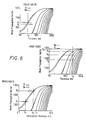
- Figure 6 shows the variation of the mode propagation vector of radiation propagating along a waveguide with waveguide thickness for differing polarisations, mode orders and wavelengths.
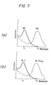
- Figure 7 shows schematic absorption peaks for assays involving two different wavelengths of exciting radiation
- Figure 8 shows a waveguide with a planar, circular geometry.
- Figure 9 shows (a) a profile of a photolithography mask and (b) the grating profile which results according to the method exemplified hereinafter in Example 1.
- Figure 10 shows schematically an apparatus suitable for carrying out an assay in connection with the present invention, as exemplified hereinafter in Example 2.
- Figure 1(a) shows a waveguide 2 with a grating 4 at one end providing input coupling of the exciting radiation 6.
- the grating 4 exhibits angular discrimination of wavelength and mode order thereby permitting a high degree of control over the excitation process.
- a transduction region 8 is disposed on the surface of the waveguide 2.
- a grating 10 provides selective reflection of the exciting radiation.
- the exciting radiation traverses the transduction region 8 twice, thereby increasing and making more uniform the radiation intensity in the transduction region.
- the radiation is attenuated by absorption as it propagates along the waveguide 2 as is shown in the graph of radiation intensity versus position along transduction region in Figure 1 (b). This graph shows the attenuation for both the first pass 12 and second pass 14 of the radiation together with the resulting total intensity 16.
- FIG. 2 illustrates another waveguide configuration.
- a grating 20 input-couples the exciting radiation 22 into the waveguide 24.
- the transduction region 26 is such that signal radiation 28 of a different wavelength to the exciting radiation 22 is coupled into the waveguide 24.
- a second grating 30 selectively reflects the exciting radiation 22 and as described above increases and makes more uniform the intensity of the exciting radiation of the transduction region 26.
- Another grating 32 selectively reflects the signal radiation 28.
- a further grating 34 output-couples the signal radiation from the waveguide 24.
- Grating 32 serves to increase the amount of signal radiation 28 reaching grating 34 and thus being output-coupled from the waveguide 24.
- Grating 20 also serves to reduce the amount of exciting radiation 22 reaching the grating 34.
- gratings 30 and 32 could be used to reflect specific polarisations or modes of the radiation.
- Grating 32 could also incorporate an output-coupling function for the exciting radiation 22. If, say, 5% of the exciting radiation 22 within the waveguide 24 were output-coupled by grating 32 then this could be used as a reference signal for calibration/scaling.
- Figures 3(a),(b) and (c) The use of gratings to deform spatially the radiation within the waveguide is illustrated in Figures 3(a),(b) and (c). These figures illustrate how it is possible to achieve angular discrimination between wavelengths, polarisations, mode orders and the incidence direction of radiation.
- Figure 3a shows angular discrimination in the plane perpendicular to the waveguide.
- Figure 3b shows angular discrimination in the plane parallel to the waveguide.
- Figure 3c shows how radiation of differing wavelength/mode/polarisation may be focused to different points outside the waveguide. Radiation may also be focused to a point within the waveguide as is shown in Figure 5.
- FIG 4 illustrates a simple application of the property shown in figure 3.
- Grating 40 is used to input-couple exciting radiation originating from a point source 42 into a waveguide 44 (no external optics are needed). The exciting radiation then traverses the transduction region 46 and reflects off grating 48.
- Figure 5 shows a waveguide using intra-waveguide focusing.
- Exciting radiation from point source 50 is input-coupled to the waveguide 52 by grating 54.
- Grating 54 also has the function of causing the radiation to converge.
- the radiation then traverses transduction region 56.
- the radiation reflects off grating 58, the radiation having a focal point within the waveguide 52 at a point which also happens to be within grating 58.
- the radiation then once more traverses the transduction region 56 to reach grating 60.
- Grating 60 serves to output-couple the radiation from the grating 58 and focus it to a point 62.
- Figure 6 shows the variation in mode propagation vector of radiation propagating along a waveguide with waveguide thickness for differing polarisations, mode orders and wavelengths.
- the discrimination of the grating structures described above is achieved by exploiting the phenomena illustrated in these graphs so that the grating structures selectively interact with radiation having certain propagation characteristics.
- the interaction in the transduction region is dependent on mode order/polarisation/wavelength then the differential analysis of the signals for a set of modes is a useful method of detection when the waveguide modes can be accurately controlled.
- a waveguide according to the invention may employ two different wavelengths of exciting radiation.
- exciting radiation with wavelength ⁇ 1 is input-coupled at a first angle by a first grating whilst exciting radiation with a different wavelength ⁇ 2 is input-coupled at a second angle by the same grating.
- the radiation then propagates along the waveguide, is reflected by a second grating such that it traverses the transduction region twice, and is output-coupled by a third grating at an angle dependent on wavelength.
- Absorption peaks at different wavelengths for use in multiple analyte assays are shown in Figure 7(a).
- a shift in absorption of a single analyte could be monitored as illustrated in Figure 7(b).
- Figure 8 shows a waveguide with a circular planar geometry.
- Figure 8(a) is an elevation;
- Figure 8(b) is a plan view.
- Strips 88 which may be made of glue, separate the different transduction regions.
- This waveguide is particularly suited to the use of multiple transduction regions and can also benefit from the intensity profile of focused radiation to reduce the effect of absorption as described above.
- Example although not itself an illustration of the invention, illustrates how one may fabricate a grating such as those which may be found on a waveguide of the present invention.
- a solution of 1M iron (III) nitrate (BDH, Poole, UK), 1M phosphoric acid (BDH, Poole, UK) and methanol (BDH, Poole, UK) was applied to a large face of a glass microscope slide having dimensions 52mm x 75mm x 1.5mm (Gallenkamp, UK).
- the coated slide was spun at 1000 rpm for 2 minutes.
- a photolithography mask having a rectangular grating profile of pitch approximately 21 micrometres and depth 70nm (RAL, Daresbury, UK) was pressed using finger pressure into the iron (III) phosphate film, which was still soft, on the glass side.
- the coated slide was then baked for 1 hour at 200°C.
- the resulting hard glassy film on the slide was found to have a refractive index of 1.72.
- the surface profile (Taly step trace) of a grating fabricated by this method is shown diagrammatically in Figure 9(b), below a profile of the photolithography mask described hereinabove, for comparison, Figure 9(a).
- Embossed iron (III) phosphate films of the type described may be used either as overlays on a waveguide surface or as intrinsic waveguides when deposited on substrates having a refractive index less than 1.72 (e.g. Permabloc, Pilkington Glass Ltd., St. Helens, UK).
- An appropriate reagent can be immobilised on a region of the waveguide in conventional manner.
- a waveguide incorporating gratings fabricated according to Example 1 may be used in the assay to be described, wherein fluorescently labelled antibody becomes bound as a result of formation of a sandwich complex with the analyte ligand (hCG) and a second antibody already immobilised at the test region of the waveguide surface.
- test region of a waveguide incorporating gratings fabricated according to the method of Example 1 is activated with a silane (8% 3-glycidoxypropyltrimethoxysilane) at pH 3.5 for 2 hours.
- silane 8% 3-glycidoxypropyltrimethoxysilane
- an appropriate crosslinking agent e.g. SMCC, succinimidyl 4-(N-maleimidomethyl)cyclohexane-1-carboxylate, or glutaraldehyde
- the waveguide is then spin-coated with a 10% sucrose, 0.1% casein layer and stored under dry conditions at 4°C until use.
- Monoclonal anti-hCG antibodies are obtained from mouse ascites fluid by the method of Milstein and Kohler in Nature 256 , 495-497 (1975). Antibodies from individual hybridoma cell lines are screened to identify those producing antibody to discrete antigen determinants. Antibodies having the highest affinities to hCG are selected for use in the assay. 20 mg of XRITC are dissolved in 2 ml of methanol and the resulting solution is made up to 20 ml with a buffer solution of 0.2 M sodium bicarbonate (pH9). This solution is then mixed with 2 mg of anti-hCG antibody and left to react for 19.5 hours. Finally, the solution is purified using a Pharmacia PD10 column and employing 0.2 M sodium bicarbonate buffer.
- a freeze-dried preparation of hCG, calibrated against the first international reference preparation (75/537) is diluted in a phosphate buffer solution (pH 7.3) to the desired concentration.
- the light source 91 is a 1 mW helium/neon laser (Melles Griot, USA) producing a beam of radiation at 543.5 nm.
- the beam passes through an interference filter 92 (546.1 nm, bandwidth 10 nm) and then through a polariser 93, in order selectively to excite the TE mode of the optical waveguide 94, which is present on the surface of a substrate 95.
- Mounted on the waveguide is a prism 96 (an equilateral prism of LAF788474 glass having a refractive index of 1.792 at 543.5 nm (IC Optical Systems, Beckenham, UK)).
- Fluorescence signal produced during the assay is filtered by a long-pass collection filter 97 with a cut-on at 600.2 nm (Ealing Electro-optics, Ealing, UK) and is then detected by a Hakuto R928 photomultiplier tube 98 (Hakuto, Waltham Cross, UK).
- An EG and G 5207 lock-in amplifier 99 is used to retrieve the signal from the photomultiplier tube and is connected to a chopper 100 which modulates the laser output.
- a glass cover 101 is used to form a cell cavity of sufficiently small dimensions to enable sample to be drawn into contact with the test region of the waveguide by capillary action.
- the apparatus is calibrated by recording the signal from the photomultiplier tube 98 at 30 second intervals over a period of 8 minutes for zero and known concentrations of hCG and at a fixed, known concentration (excess) of XRITC-conjugated anti-hCG antibody. Assays are then carried out by following the same procedure, but using analyte solutions in which the concentrations of hCG are unknown, and comparing the results with the calibration curves.
Landscapes
- Physics & Mathematics (AREA)
- Chemical & Material Sciences (AREA)
- Pathology (AREA)
- General Physics & Mathematics (AREA)
- Plasma & Fusion (AREA)
- Health & Medical Sciences (AREA)
- Life Sciences & Earth Sciences (AREA)
- Analytical Chemistry (AREA)
- Biochemistry (AREA)
- General Health & Medical Sciences (AREA)
- Engineering & Computer Science (AREA)
- Immunology (AREA)
- Chemical Kinetics & Catalysis (AREA)
- Investigating, Analyzing Materials By Fluorescence Or Luminescence (AREA)
- Geophysics And Detection Of Objects (AREA)
- Investigating Or Analysing Materials By Optical Means (AREA)
- Investigating Or Analyzing Materials By The Use Of Fluid Adsorption Or Reactions (AREA)
- Investigating Or Analyzing Materials By The Use Of Ultrasonic Waves (AREA)
- Fire-Detection Mechanisms (AREA)
- Measuring Fluid Pressure (AREA)
- Cable Accessories (AREA)
- Air Bags (AREA)
- Photoreceptors In Electrophotography (AREA)
- Investigating Or Analysing Materials By The Use Of Chemical Reactions (AREA)
- Optical Integrated Circuits (AREA)
Claims (13)
- Détecteur de guide d'ondes comportant deux structures de grille optique, caractérisé en ce qu'au moins une des structures de grille est capable de réfléchir un rayonnement se déplaçant le long du guide d'ondes, de sorte que ce rayonnement parcourt au moins deux fois la région comprise entre les deux structures de grille.
- Guide d'ondes suivant la revendication 1, ayant une épaisseur comprise entre 0,2 et 10,0 µm.
- Guide d'ondes suivant la revendication 1 ou la revendication 2, caractérisé en ce qu'il comporte au moins une autre structure de grille optique.
- Guide d'ondes suivant une quelconque des revendications précédentes, qui est sensiblement plan.
- Guide d'ondes suivant la revendication 4, qui est sensiblement circulaire et dans lequel les structures de grille sont disposées concentriquement.
- Guide d'ondes suivant la revendication 5, dans lequel il est prévu des bandes radiales.
- Guide d'ondes suivant une quelconque des revendications 1 à 6, dans lequel au moins une structure de grille est capable de filtrer ledit rayonnement en fonction des différences de longueur d'onde, de polarisation ou de mode dudit rayonnement.
- Guide d'ondes suivant une quelconque des revendications 1 à 6, dans lequel au moins une structure de grille est capable de coupler ledit rayonnement à la sortie dudit guide d'ondes, et/ou est capable de coupler le rayonnement appliqué à l'entrée dans ledit guide d'ondes.
- Guide d'ondes suivant une quelconque des revendications 1 à 6, dans lequel au moins une structure de grille est capable de provoquer la convergence, la divergence ou la collimation du rayonnement qui est appliqué à ladite structure de grille ou du rayonnement qui se propage le long dudit guide d'ondes.
- Guide d'ondes suivant la revendication 1 ou la revendication 2, pour l'utilisation dans une analyse, dans lequel une matière, qui peut se lier spécifiquement à un élément à analyser, est immobilisée directement ou indirectement sur la région comprise entre les deux structures de grille.
- Utilisation dans une analyse d'un guide d'ondes suivant une quelconque des revendications précédentes.
- Méthode d'analyse pour un ligand dans un échantillon, ladite méthode comprenant l'incubation, simultanément ou dans toute séquence désirée, de l'échantillon en association avec :(a) un partenaire de liaison spécifique pour le ligand qu'on désire détecter, et(b) un autre réactif qui est un ligand analogue ou un partenaire de liaison spécifique dudit ligand,un des composants (a) et (b) étant immobilisé, directement ou indirectement, sur la surface de la région comprise entre les deux structures de grille d'un guide d'ondes suivant une quelconque des revendications 1 à 10, et l'autre des composants (a) et (b) portant un marqueur fluorescent ;
et la détermination de ce que le marqueur fluorescent devient ou non indirectement immobilisé sur ladite région comme résultat de la formation d'un complexe et, si on le désire, de l'étendue et/ou de la vitesse auxquelles cela se produit. - Méthode d'analyse pour un ligand dans un échantillon, ladite méthode comprenant l'incubation, simultanément ou dans toute séquence désirée, de l'échantillon en association avec :(a) un partenaire de liaison spécifique pour le ligand qu'on désire détecter, et(b) un autre réactif, qui est un ligand analogue ou un partenaire de liaison spécifique dudit ligand,un des composants (a) et (b) étant immobilisé, directement ou indirectement, sur la surface de la région comprise entre les deux structures de grille d'un guide d'ondes suivant une quelconque des revendications 1 à 10, le composant immobilisé (a) ou (b) ou la surface de la dite région portant un fluorophore, et l'autre des composants (a) et (b) étant tel que, lors de la formation d'un complexe, la fluorescence dudit fluorophore est éteinte ;
et ladite méthode comprenant l'étape de détermination de ce que la fluorescence dudit fluorophore est éteinte comme résultat de la formation d'un complexe, et, si on le désire, de l'étendue et/ou de la vitesse auxquelles cela se produit.
Applications Claiming Priority (3)
| Application Number | Priority Date | Filing Date | Title |
|---|---|---|---|
| GB8807486 | 1988-03-29 | ||
| GB888807486A GB8807486D0 (en) | 1988-03-29 | 1988-03-29 | Waveguide sensor |
| PCT/GB1989/000321 WO1989009394A1 (fr) | 1988-03-29 | 1989-03-28 | Detecteur de guide d'ondes |
Publications (2)
| Publication Number | Publication Date |
|---|---|
| EP0363467A1 EP0363467A1 (fr) | 1990-04-18 |
| EP0363467B1 true EP0363467B1 (fr) | 1994-10-05 |
Family
ID=10634313
Family Applications (1)
| Application Number | Title | Priority Date | Filing Date |
|---|---|---|---|
| EP89904169A Expired - Lifetime EP0363467B1 (fr) | 1988-03-29 | 1989-03-28 | Detecteur de guide d'ondes |
Country Status (10)
| Country | Link |
|---|---|
| US (1) | US5081012A (fr) |
| EP (1) | EP0363467B1 (fr) |
| JP (1) | JPH087139B2 (fr) |
| AT (1) | ATE112626T1 (fr) |
| AU (1) | AU612827B2 (fr) |
| CA (1) | CA1314743C (fr) |
| DE (1) | DE68918659T2 (fr) |
| GB (1) | GB8807486D0 (fr) |
| NO (1) | NO178708C (fr) |
| WO (1) | WO1989009394A1 (fr) |
Families Citing this family (80)
| Publication number | Priority date | Publication date | Assignee | Title |
|---|---|---|---|---|
| US5082629A (en) * | 1989-12-29 | 1992-01-21 | The Board Of The University Of Washington | Thin-film spectroscopic sensor |
| US5407829A (en) * | 1990-03-27 | 1995-04-18 | Avl Medical Instruments Ag | Method for quality control of packaged organic substances and packaging material for use with this method |
| EP0455067B1 (fr) * | 1990-05-03 | 2003-02-26 | F. Hoffmann-La Roche Ag | Capteur microoptique |
| GB9019999D0 (en) * | 1990-09-13 | 1990-10-24 | Amersham Int Plc | Biological sensors |
| DE4128846C2 (de) * | 1991-08-30 | 1994-07-14 | Rainer Dr Klein | Integriert optischer Stoffsensor |
| ATE226320T1 (de) * | 1993-03-26 | 2002-11-15 | Hoffmann La Roche | Optisches verfahren und vorrichtung zur analyse von substanzen an sensoroberflächen |
| US5919712A (en) | 1993-05-18 | 1999-07-06 | University Of Utah Research Foundation | Apparatus and methods for multi-analyte homogeneous fluoro-immunoassays |
| US5512492A (en) * | 1993-05-18 | 1996-04-30 | University Of Utah Research Foundation | Waveguide immunosensor with coating chemistry providing enhanced sensitivity |
| US5677196A (en) * | 1993-05-18 | 1997-10-14 | University Of Utah Research Foundation | Apparatus and methods for multi-analyte homogeneous fluoro-immunoassays |
| MXPA96005828A (es) * | 1994-05-27 | 2005-07-15 | Novartis Ag Tambien Denominada | Proceso para detectar luminescencia excitada evanescentemente. |
| SE510733C2 (sv) | 1995-01-03 | 1999-06-21 | Chemel Ab | Kemisk sensor baserad på utbytbar igenkänningskomponent samt användning därav |
| US5814565A (en) * | 1995-02-23 | 1998-09-29 | University Of Utah Research Foundation | Integrated optic waveguide immunosensor |
| KR19990014709A (ko) | 1995-05-12 | 1999-02-25 | 한스루돌프하우스 | 센서 플랫폼 및 감쇠 여기된 발광을 이용한 복수 분석물의병렬 검출 방법 |
| JP3236199B2 (ja) * | 1995-08-25 | 2001-12-10 | 日本電気株式会社 | 平面光導波路型バイオケミカルセンサ |
| DE69733650T2 (de) * | 1996-03-01 | 2006-04-20 | Beckman Coulter, Inc., Fullerton | System zum simultanen Durchführen einer Vielzahl von Ligandenbindungs-Untersuchungen |
| EP0888546A1 (fr) * | 1996-03-19 | 1999-01-07 | University Of Utah Research Foundation | Appareil d'oscillation et methodes d'immunodosage fluorescent homogene a plusieurs echantillons a analyser |
| US6211954B1 (en) | 1996-03-30 | 2001-04-03 | Novartis Ag | Integrated optical luminescence sensor |
| US5832165A (en) | 1996-08-28 | 1998-11-03 | University Of Utah Research Foundation | Composite waveguide for solid phase binding assays |
| WO1998009156A1 (fr) * | 1996-08-29 | 1998-03-05 | Novartis Ag | Capteur optique chimique/biochimique |
| US6222619B1 (en) | 1997-09-18 | 2001-04-24 | University Of Utah Research Foundation | Diagnostic device and method |
| JP3086674B2 (ja) * | 1998-02-20 | 2000-09-11 | アヴェンティス・リサーチ・ウント・テクノロジーズ・ゲーエムベーハー・ウント・コー・カーゲー | 指度校正を可能にする有機物質検出装置及びそれを用いた有機物質監視システム |
| FR2778986B1 (fr) * | 1998-05-22 | 2000-07-21 | Suisse Electronique Microtech | Capteur optique utilisant une reaction immunologique et un marqueur fluorescent |
| US6661942B1 (en) | 1998-07-20 | 2003-12-09 | Trans Photonics, Llc | Multi-functional optical switch (optical wavelength division multiplexer/demultiplexer, add-drop multiplexer and inter-connect device) and its methods of manufacture |
| JP2003501654A (ja) * | 1999-06-05 | 2003-01-14 | ツェプトゼンス アクチエンゲゼルシャフト | 複数の分析対象物の測定のためのセンサプラットフォーム及び方法 |
| ATE299589T1 (de) † | 1999-08-20 | 2005-07-15 | Diagnostische Forsch Stiftung | Verfahren zur bestimmung von substanzen mittels der evaneszenzfeldmethode |
| EP1085315B1 (fr) * | 1999-09-15 | 2003-07-09 | CSEM Centre Suisse d'Electronique et de Microtechnique SA | Capteur optique intégré |
| US6330064B1 (en) * | 2000-03-13 | 2001-12-11 | Satcon Technology Corporation | Doubly-differential interferometer and method for evanescent wave surface detection |
| US7158224B2 (en) * | 2000-06-25 | 2007-01-02 | Affymetrix, Inc. | Optically active substrates |
| US20080220440A1 (en) * | 2000-07-25 | 2008-09-11 | M Selim Unlu | Waveguide sensors optimized for discrimination against non-specific binding |
| WO2002033005A2 (fr) * | 2000-10-19 | 2002-04-25 | Trans Photonics, L.L.C. | Nouveaux composants chromophoriques polyaryl-substitues |
| US6694067B1 (en) * | 2001-01-05 | 2004-02-17 | Los Gatos Research | Cavity enhanced fiber optic and waveguide chemical sensor |
| US7029631B2 (en) * | 2002-04-19 | 2006-04-18 | Agilent Technologies, Inc. | Apparatus for improved light collection |
| US20030232427A1 (en) * | 2002-06-18 | 2003-12-18 | Montagu Jean I. | Optically active substrates for examination of biological materials |
| US7441703B2 (en) | 2002-08-20 | 2008-10-28 | Illumina, Inc. | Optical reader for diffraction grating-based encoded optical identification elements |
| JP2005536769A (ja) * | 2002-08-20 | 2005-12-02 | シヴェラ コーポレイション | 回折格子をベースとする光学同定要素 |
| US7900836B2 (en) * | 2002-08-20 | 2011-03-08 | Illumina, Inc. | Optical reader system for substrates having an optically readable code |
| US7619819B2 (en) * | 2002-08-20 | 2009-11-17 | Illumina, Inc. | Method and apparatus for drug product tracking using encoded optical identification elements |
| US20050227252A1 (en) * | 2002-08-20 | 2005-10-13 | Moon John A | Diffraction grating-based encoded articles for multiplexed experiments |
| US7190522B2 (en) * | 2002-09-12 | 2007-03-13 | Cyvera Corporation | Chemical synthesis using diffraction grating-based encoded optical elements |
| WO2004019277A1 (fr) * | 2002-08-20 | 2004-03-04 | Cyvera Corporation | Microparticules codees basees sur un reseau de diffraction pour experiences multiplexees |
| US7901630B2 (en) * | 2002-08-20 | 2011-03-08 | Illumina, Inc. | Diffraction grating-based encoded microparticle assay stick |
| US7872804B2 (en) * | 2002-08-20 | 2011-01-18 | Illumina, Inc. | Encoded particle having a grating with variations in the refractive index |
| US20040126875A1 (en) * | 2002-09-12 | 2004-07-01 | Putnam Martin A. | Assay stick |
| US7399643B2 (en) * | 2002-09-12 | 2008-07-15 | Cyvera Corporation | Method and apparatus for aligning microbeads in order to interrogate the same |
| US7923260B2 (en) | 2002-08-20 | 2011-04-12 | Illumina, Inc. | Method of reading encoded particles |
| US7508608B2 (en) * | 2004-11-17 | 2009-03-24 | Illumina, Inc. | Lithographically fabricated holographic optical identification element |
| US7164533B2 (en) * | 2003-01-22 | 2007-01-16 | Cyvera Corporation | Hybrid random bead/chip based microarray |
| US20100255603A9 (en) | 2002-09-12 | 2010-10-07 | Putnam Martin A | Method and apparatus for aligning microbeads in order to interrogate the same |
| EP1540591A1 (fr) * | 2002-09-12 | 2005-06-15 | Cyvera Corporation | Microparticules codees sur la base d'un reseau de diffraction pour experimentations multiplexees |
| CA2499037A1 (fr) * | 2002-09-12 | 2004-03-25 | Cyvera Corporation | Procede et appareil d'etiquetage utilisant des elements d'identification optique codes a reseau de diffraction |
| US7092160B2 (en) | 2002-09-12 | 2006-08-15 | Illumina, Inc. | Method of manufacturing of diffraction grating-based optical identification element |
| US7027163B2 (en) * | 2003-01-24 | 2006-04-11 | General Dynamics Advanced Information Systems, Inc. | Grating sensor |
| US7445938B2 (en) * | 2003-01-24 | 2008-11-04 | General Dynamics Advanced Information Systems, Inc. | System and method for detecting presence of analytes using gratings |
| US20060057729A1 (en) * | 2003-09-12 | 2006-03-16 | Illumina, Inc. | Diffraction grating-based encoded element having a substance disposed thereon |
| DE10353694A1 (de) * | 2003-11-18 | 2005-06-30 | Fraunhofer-Gesellschaft zur Förderung der angewandten Forschung e.V. | Mikroskopievorrichtung |
| US7433123B2 (en) * | 2004-02-19 | 2008-10-07 | Illumina, Inc. | Optical identification element having non-waveguide photosensitive substrate with diffraction grating therein |
| US7410614B2 (en) * | 2004-07-26 | 2008-08-12 | Kabushiki Kaisha Toshiba | Optical waveguide type iontophoresis sensor chip and method for packaging sensor chip |
| US7709247B2 (en) * | 2004-08-04 | 2010-05-04 | Intel Corporation | Methods and systems for detecting biomolecular binding using terahertz radiation |
| US7604173B2 (en) * | 2004-11-16 | 2009-10-20 | Illumina, Inc. | Holographically encoded elements for microarray and other tagging labeling applications, and method and apparatus for making and reading the same |
| EP2194485B1 (fr) | 2004-11-16 | 2012-10-17 | Illumina, Inc. | Procédés et appareils pour la lecture de microbilles codées |
| WO2006055735A2 (fr) | 2004-11-16 | 2006-05-26 | Illumina, Inc | Scanner dote d'un modulateur spatial de lumiere |
| US7623624B2 (en) * | 2005-11-22 | 2009-11-24 | Illumina, Inc. | Method and apparatus for labeling using optical identification elements characterized by X-ray diffraction |
| US9528939B2 (en) | 2006-03-10 | 2016-12-27 | Indx Lifecare, Inc. | Waveguide-based optical scanning systems |
| US8675199B2 (en) * | 2006-03-10 | 2014-03-18 | Plc Diagnostics, Inc. | Waveguide-based detection system with scanning light source |
| US9423397B2 (en) | 2006-03-10 | 2016-08-23 | Indx Lifecare, Inc. | Waveguide-based detection system with scanning light source |
| US8288157B2 (en) * | 2007-09-12 | 2012-10-16 | Plc Diagnostics, Inc. | Waveguide-based optical scanning systems |
| US9976192B2 (en) | 2006-03-10 | 2018-05-22 | Ldip, Llc | Waveguide-based detection system with scanning light source |
| US7830575B2 (en) * | 2006-04-10 | 2010-11-09 | Illumina, Inc. | Optical scanner with improved scan time |
| BRPI0714970A2 (pt) * | 2006-07-20 | 2013-05-07 | Koninkl Philips Electronics Nv | sistema de detecÇço para detectar luminescÊncia de pelo menos uma amostra quando excitada atravÉs de radiaÇço de excitaÇço incidente, e, mÉtodo para detectar luminescÊncia de pelo menos uma amostra. |
| US20090124024A1 (en) * | 2007-11-07 | 2009-05-14 | Shingo Kasai | Optical-waveguide sensor chip, method of manufacturing the same, method of measuring substance, substance-measuring kit and optical-waveguide sensor |
| GB2461026B (en) * | 2008-06-16 | 2011-03-09 | Plc Diagnostics Inc | System and method for nucleic acids sequencing by phased synthesis |
| US8218151B2 (en) * | 2009-03-12 | 2012-07-10 | Tel Aviv University Future Technology Development Ltd | Light-emitting intra-cavity interferometric sensors |
| DE102009055737A1 (de) * | 2009-11-25 | 2011-05-26 | Friedrich-Schiller-Universität Jena | Optische Vorrichtung zur Erzeugung einer störfähigen internen Totalreflexion und deren Verwendung |
| JP2013238541A (ja) * | 2012-05-16 | 2013-11-28 | Toshiba Corp | 光導波路型測定システムおよび糖化ヘモグロビンの測定方法 |
| EP2824446A1 (fr) * | 2013-07-12 | 2015-01-14 | F. Hoffmann-La Roche AG | Dispositif à utiliser pour la détection des affinités de liaison |
| US10018566B2 (en) | 2014-02-28 | 2018-07-10 | Ldip, Llc | Partially encapsulated waveguide based sensing chips, systems and methods of use |
| WO2016138427A1 (fr) | 2015-02-27 | 2016-09-01 | Indx Lifecare, Inc. | Système de détection à guide d'ondes à source de lumière à balayage |
| US9851290B2 (en) | 2015-06-22 | 2017-12-26 | Sharp Laboratories Of America, Inc. | Particle detector for particulate matter accumulated on a surface |
| CN107850537B (zh) * | 2015-06-30 | 2020-05-19 | Imec 非营利协会 | 辐射载体及其在光学传感器中的使用 |
| WO2017005621A1 (fr) | 2015-07-07 | 2017-01-12 | Agc Glass Europe | Substrat de verre doté de meilleures résistances aux intempéries et aux produits chimiques |
Family Cites Families (8)
| Publication number | Priority date | Publication date | Assignee | Title |
|---|---|---|---|---|
| US4550017A (en) * | 1982-10-15 | 1985-10-29 | Syntex (U.S.A.) Inc. | Fluorescence screening for blood typing |
| JPS60236006A (ja) * | 1984-05-10 | 1985-11-22 | Nec Corp | 線巾測定方法 |
| JPH0660876B2 (ja) * | 1985-03-30 | 1994-08-10 | 株式会社東芝 | 分析装置 |
| WO1986007149A1 (fr) * | 1985-05-29 | 1986-12-04 | Kurt Tiefenthaler | Senseur optique pour etablir selectivement la presence de substances ainsi que la variation d'indice de refraction dans les substances objet de mesures |
| US4671938A (en) * | 1985-09-09 | 1987-06-09 | Ciba-Corning Diagnostics, Corp. | Immunoassay apparatus |
| DE3723159A1 (de) * | 1986-07-17 | 1988-01-21 | Prosumus Ag | Chemosensor sowie mit diesem durchfuehrbare verfahren |
| EP0275275B1 (fr) * | 1986-07-17 | 1992-05-20 | PROSUMUS AG Elektronisch-mechanische Geräte | Chemosenseur |
| AU604364B2 (en) * | 1987-08-13 | 1990-12-13 | Dow Chemical Company, The | Sulfur dioxide removal from gas streams using hydroxyalkyl substituted piperazinones |
-
1988
- 1988-03-29 GB GB888807486A patent/GB8807486D0/en active Pending
-
1989
- 1989-03-28 AU AU33603/89A patent/AU612827B2/en not_active Expired
- 1989-03-28 EP EP89904169A patent/EP0363467B1/fr not_active Expired - Lifetime
- 1989-03-28 CA CA000594928A patent/CA1314743C/fr not_active Expired - Lifetime
- 1989-03-28 JP JP1503800A patent/JPH087139B2/ja not_active Expired - Fee Related
- 1989-03-28 AT AT89904169T patent/ATE112626T1/de not_active IP Right Cessation
- 1989-03-28 WO PCT/GB1989/000321 patent/WO1989009394A1/fr not_active Ceased
- 1989-03-28 DE DE68918659T patent/DE68918659T2/de not_active Expired - Lifetime
- 1989-11-28 NO NO894745A patent/NO178708C/no not_active IP Right Cessation
-
1990
- 1990-01-22 US US07/435,519 patent/US5081012A/en not_active Expired - Lifetime
Also Published As
| Publication number | Publication date |
|---|---|
| JPH02504313A (ja) | 1990-12-06 |
| ATE112626T1 (de) | 1994-10-15 |
| NO894745L (no) | 1990-01-26 |
| CA1314743C (fr) | 1993-03-23 |
| DE68918659T2 (de) | 1995-02-09 |
| DE68918659D1 (de) | 1994-11-10 |
| GB8807486D0 (en) | 1988-05-05 |
| WO1989009394A1 (fr) | 1989-10-05 |
| NO178708B (no) | 1996-02-05 |
| EP0363467A1 (fr) | 1990-04-18 |
| AU3360389A (en) | 1989-10-16 |
| NO894745D0 (no) | 1989-11-28 |
| AU612827B2 (en) | 1991-07-18 |
| NO178708C (no) | 1996-05-15 |
| JPH087139B2 (ja) | 1996-01-29 |
| US5081012A (en) | 1992-01-14 |
Similar Documents
| Publication | Publication Date | Title |
|---|---|---|
| EP0363467B1 (fr) | Detecteur de guide d'ondes | |
| US5478755A (en) | Long range surface plasma resonance immunoassay | |
| US5830766A (en) | Enhanced signal-to-noise ratio and sensitivity optical immunoassay | |
| US5344784A (en) | Fluorescent assay and sensor therefor | |
| EP0205236B1 (fr) | Capteurs biologiques à guides d'ondes optiques | |
| US5814565A (en) | Integrated optic waveguide immunosensor | |
| US5822472A (en) | Process for detecting evanescently excited luminescence | |
| US4877747A (en) | Optical assay: method and apparatus | |
| US6395558B1 (en) | Optical chemical/biochemical sensor | |
| EP0851230B1 (fr) | Procédé et appareil pour le dosage immunologique utilisant la résonance plasmonique de surface induite par fluorescence | |
| US6483096B1 (en) | Integrated-optical chemical and biochemical sensor | |
| EP0382832B1 (fr) | Methode d'analyse d'un ligand dans un echantillon | |
| EP0543831A1 (fr) | Dispositif analyseur. | |
| WO1992014140A1 (fr) | Dispositif d'analyse | |
| EP0321523B1 (fr) | Detecteur utilisant un guide d'ondes | |
| Kunz et al. | Sensing pads for hybrid and monolithic integrated optical immunosensors | |
| JP2004184381A (ja) | 光導波路型表面プラズモン共鳴センサおよび光導波路型表面プラズモン共鳴装置 | |
| Walczak et al. | Sensitive fiber-optic immunoassay | |
| Christensen et al. | Optical immunoassay systems based upon evanescent wave interactions | |
| JPH06117997A (ja) | 光学的測定装置 | |
| Zhou | The Development of an Optical Immunosensor Based on Ion-Exchanged Waveguides in Glass and Evanescent Excitation of Fluorescence |
Legal Events
| Date | Code | Title | Description |
|---|---|---|---|
| PUAI | Public reference made under article 153(3) epc to a published international application that has entered the european phase |
Free format text: ORIGINAL CODE: 0009012 |
|
| AK | Designated contracting states |
Kind code of ref document: A1 Designated state(s): AT BE CH DE FR GB IT LI LU NL SE |
|
| 17P | Request for examination filed |
Effective date: 19900320 |
|
| 17Q | First examination report despatched |
Effective date: 19910510 |
|
| RAP1 | Party data changed (applicant data changed or rights of an application transferred) |
Owner name: APPLIED RESEARCH SYSTEMS ARS HOLDING N.V. |
|
| RAP1 | Party data changed (applicant data changed or rights of an application transferred) |
Owner name: ARS HOLDING 89 N.V |
|
| GRAA | (expected) grant |
Free format text: ORIGINAL CODE: 0009210 |
|
| AK | Designated contracting states |
Kind code of ref document: B1 Designated state(s): AT BE CH DE FR GB IT LI LU NL SE |
|
| REF | Corresponds to: |
Ref document number: 112626 Country of ref document: AT Date of ref document: 19941015 Kind code of ref document: T |
|
| ITF | It: translation for a ep patent filed | ||
| REF | Corresponds to: |
Ref document number: 68918659 Country of ref document: DE Date of ref document: 19941110 |
|
| ET | Fr: translation filed | ||
| EAL | Se: european patent in force in sweden |
Ref document number: 89904169.3 |
|
| PLBE | No opposition filed within time limit |
Free format text: ORIGINAL CODE: 0009261 |
|
| STAA | Information on the status of an ep patent application or granted ep patent |
Free format text: STATUS: NO OPPOSITION FILED WITHIN TIME LIMIT |
|
| 26N | No opposition filed | ||
| REG | Reference to a national code |
Ref country code: GB Ref legal event code: 732E |
|
| NLS | Nl: assignments of ep-patents |
Owner name: APPLIED RESEARCH SYSTEMS ARS HOLDING N.V. |
|
| REG | Reference to a national code |
Ref country code: CH Ref legal event code: PUE Owner name: ARS HOLDING 89 N.V. TRANSFER- APPLIED RESEARCH SYS |
|
| REG | Reference to a national code |
Ref country code: FR Ref legal event code: TP |
|
| BECA | Be: change of holder's address |
Free format text: 960508 *APPLIED RESEARCH SYSTEMS ARS (HOLDING) N.V.:JOHN B. GORSIRAWEG 14, CURACAO |
|
| REG | Reference to a national code |
Ref country code: GB Ref legal event code: IF02 |
|
| PGFP | Annual fee paid to national office [announced via postgrant information from national office to epo] |
Ref country code: CH Payment date: 20080313 Year of fee payment: 20 |
|
| PGFP | Annual fee paid to national office [announced via postgrant information from national office to epo] |
Ref country code: LU Payment date: 20080328 Year of fee payment: 20 Ref country code: IT Payment date: 20080327 Year of fee payment: 20 Ref country code: SE Payment date: 20080306 Year of fee payment: 20 Ref country code: NL Payment date: 20080203 Year of fee payment: 20 |
|
| REG | Reference to a national code |
Ref country code: CH Ref legal event code: PFA Owner name: APPLIED RESEARCH SYSTEMS ARS HOLDING N.V. Free format text: APPLIED RESEARCH SYSTEMS ARS HOLDING N.V.#14 JOHN B. GORSIRAWEG#CURACAO (AN) -TRANSFER TO- APPLIED RESEARCH SYSTEMS ARS HOLDING N.V.#14 JOHN B. GORSIRAWEG#CURACAO (AN) |
|
| PGFP | Annual fee paid to national office [announced via postgrant information from national office to epo] |
Ref country code: AT Payment date: 20080313 Year of fee payment: 20 |
|
| PGFP | Annual fee paid to national office [announced via postgrant information from national office to epo] |
Ref country code: FR Payment date: 20080311 Year of fee payment: 20 Ref country code: DE Payment date: 20080407 Year of fee payment: 20 |
|
| PGFP | Annual fee paid to national office [announced via postgrant information from national office to epo] |
Ref country code: GB Payment date: 20080402 Year of fee payment: 20 |
|
| PGFP | Annual fee paid to national office [announced via postgrant information from national office to epo] |
Ref country code: BE Payment date: 20080916 Year of fee payment: 20 |
|
| BE20 | Be: patent expired |
Owner name: *APPLIED RESEARCH SYSTEMS ARS (HOLDING) N.V. Effective date: 20090328 |
|
| REG | Reference to a national code |
Ref country code: CH Ref legal event code: PL |
|
| REG | Reference to a national code |
Ref country code: GB Ref legal event code: PE20 Expiry date: 20090327 |
|
| PG25 | Lapsed in a contracting state [announced via postgrant information from national office to epo] |
Ref country code: NL Free format text: LAPSE BECAUSE OF EXPIRATION OF PROTECTION Effective date: 20090328 |
|
| NLV7 | Nl: ceased due to reaching the maximum lifetime of a patent |
Effective date: 20090328 |
|
| PG25 | Lapsed in a contracting state [announced via postgrant information from national office to epo] |
Ref country code: GB Free format text: LAPSE BECAUSE OF EXPIRATION OF PROTECTION Effective date: 20090327 |