EP0363500A1 - Circuit d'égalisation de signaux numériques reçus sous forme analogique - Google Patents
Circuit d'égalisation de signaux numériques reçus sous forme analogique Download PDFInfo
- Publication number
- EP0363500A1 EP0363500A1 EP88116127A EP88116127A EP0363500A1 EP 0363500 A1 EP0363500 A1 EP 0363500A1 EP 88116127 A EP88116127 A EP 88116127A EP 88116127 A EP88116127 A EP 88116127A EP 0363500 A1 EP0363500 A1 EP 0363500A1
- Authority
- EP
- European Patent Office
- Prior art keywords
- coefficient
- digital signals
- digital
- adder
- multiplier
- Prior art date
- Legal status (The legal status is an assumption and is not a legal conclusion. Google has not performed a legal analysis and makes no representation as to the accuracy of the status listed.)
- Granted
Links
- 238000005070 sampling Methods 0.000 claims abstract description 8
- 102100034004 Gamma-adducin Human genes 0.000 claims description 5
- 101000799011 Homo sapiens Gamma-adducin Proteins 0.000 claims description 5
- 102100024348 Beta-adducin Human genes 0.000 claims description 4
- 101000689619 Homo sapiens Beta-adducin Proteins 0.000 claims description 4
- 230000010355 oscillation Effects 0.000 claims description 3
- 230000036278 prepulse Effects 0.000 abstract 1
- 102100034033 Alpha-adducin Human genes 0.000 description 4
- 101000799076 Homo sapiens Alpha-adducin Proteins 0.000 description 4
- 101000629598 Rattus norvegicus Sterol regulatory element-binding protein 1 Proteins 0.000 description 4
- 229910004438 SUB2 Inorganic materials 0.000 description 4
- 101100311330 Schizosaccharomyces pombe (strain 972 / ATCC 24843) uap56 gene Proteins 0.000 description 4
- 238000000034 method Methods 0.000 description 4
- 101150018444 sub2 gene Proteins 0.000 description 4
- 102100036464 Activated RNA polymerase II transcriptional coactivator p15 Human genes 0.000 description 3
- 101000713904 Homo sapiens Activated RNA polymerase II transcriptional coactivator p15 Proteins 0.000 description 3
- 229910004444 SUB1 Inorganic materials 0.000 description 3
- 230000005540 biological transmission Effects 0.000 description 3
- 230000003044 adaptive effect Effects 0.000 description 2
- 238000004891 communication Methods 0.000 description 1
- 230000003111 delayed effect Effects 0.000 description 1
- 238000013461 design Methods 0.000 description 1
- 238000010586 diagram Methods 0.000 description 1
- 238000011156 evaluation Methods 0.000 description 1
- 230000002349 favourable effect Effects 0.000 description 1
- 238000012545 processing Methods 0.000 description 1
- 238000007493 shaping process Methods 0.000 description 1
Images
Classifications
-
- H—ELECTRICITY
- H04—ELECTRIC COMMUNICATION TECHNIQUE
- H04L—TRANSMISSION OF DIGITAL INFORMATION, e.g. TELEGRAPHIC COMMUNICATION
- H04L25/00—Baseband systems
- H04L25/02—Details ; arrangements for supplying electrical power along data transmission lines
- H04L25/03—Shaping networks in transmitter or receiver, e.g. adaptive shaping networks
- H04L25/03006—Arrangements for removing intersymbol interference
- H04L25/03012—Arrangements for removing intersymbol interference operating in the time domain
- H04L25/03114—Arrangements for removing intersymbol interference operating in the time domain non-adaptive, i.e. not adjustable, manually adjustable, or adjustable only during the reception of special signals
- H04L25/03133—Arrangements for removing intersymbol interference operating in the time domain non-adaptive, i.e. not adjustable, manually adjustable, or adjustable only during the reception of special signals with a non-recursive structure
Definitions
- the invention relates to a circuit arrangement according to the preamble of claim 1.
- circuit arrangements are already known (for example: NTG technical reports 88, "Ways to Integrated Communication Network", pages 50 to 57) for digital signals that are transmitted by an analog transmission method and are subject to distortions caused by pre-oscillators of subsequent digital signals as well as by post-oscillators of previously received digital signals. Strong linear distortions occur in particular in the case of digital subscriber connections in ISDN (Integrated Services Digital Network), which must be eliminated by corresponding equalization measures in digital signal receiving devices.
- the distortion caused by pre-oscillators is generally low. For example, a transversal filter with two to four fit coefficients is sufficient for equalization. In contrast, distortions caused by ringing are very large.
- equalizers can be compensated, for example, with a decision feedback equalizer.
- the number of equalizer coefficients here is in the range from 20 to 40.
- the object outlined above is achieved in a circuit arrangement according to the preamble of claim 1 by features specified in the characterizing part of this claim.
- the invention has the advantage that the post-oscillation distortions are also reduced in the pre-oscillator equalizer with little additional circuitry complexity, so that this convergence and stability behavior of the post-oscillator equalizer is improved.
- the secondary coefficients For the design of the pre-oscillator equalizer, it has proven to be expedient for the secondary coefficients to be adaptively adjustable and for the fixed factor A to be fixed at 1/2 or as an integral factor.
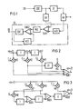
- the digital subscriber line device shown in FIG. 1 may be designed, for example, for a duplex transmission of digital signals over a two-wire line using the same method.
- a subscriber line device for example, first transmits binary signals SD to be transmitted as message signals over the two-wire line using a Encoder COD converted into multi-stage signals, for example in digital signals coded according to the 2BlQ line code and emitted as analog signals via a fork arrangement GA after pulse shaping in a pulse shaper IF.
- Analog signals to be picked up from the relevant subscriber line device via the two-wire line first pass through the already mentioned fork arrangement GA and then arrive at the digital signal receiving device EE shown in FIG.
- the input of this receiving device is formed by an analog / digital converter A / D, which takes samples from the analog signals supplied to it, for example at a distance corresponding to a bit length of the transmitted digital signals, and converts them into a predetermined number of bits.
- the necessary sampling clock pulses are provided by a clock generator, not shown.
- the digital signals provided by the analog / digital converter are then successively fed to a subtractor SUB1, which is simultaneously acted upon with compensation signals from an echo canceller EK.
- These compensation signals compensate for echo signal components contained in the digital signals, which are superimposed on the received analog signals in the previously described delivery of digital signals in analog form via the two-wire line by reflections on this line or by incomplete decoupling of the transmission paths of the fork arrangement.
- the compensated digital signals are then forwarded for further processing, if necessary via a control amplifier (not shown) to an equalizer arrangement, which largely eliminates the distortions of the digital signals caused by the electrical properties of the two-wire line.
- the equalizer arrangement has, for example, a pre-oscillator equalizer VEZ, the output of which signals are fed to a subtractor SUB2.
- a second input of this subtractor is connected to the output of a post-oscillation equalizer NEZ.
- this equalizer is connected to the output of a decision-maker ENT, which is connected downstream of the subtractor SUB2.
- the equalized digital signals ED occurring at the output of this decision-maker are then fed to further devices (not shown in FIG. 1) for further evaluation.
- FIG. 1 shows a first exemplary embodiment for the pre-oscillator equalizer VEZ shown in FIG.
- This equalizer is designed as a transversal filter, in which three successive digital signals x (n), x (n + 1) and x (n + 2) are taken into account for the equalization, which occur at the sampling times n, n + 1, n + 2 .
- These digital signals are fed to two delay elements T connected in series, each of which causes a delay time corresponding to the time interval between two successive digital signals.
- the digital signal x (n + 2) thus occurs at the input of the transversal filter simultaneously with the digital signals x (n + 1) and x (n) present at the outputs of the two delay elements T.
- These digital signals are fed to three separate multipliers M1, M2 and M3.
- the outputs of these multipliers are connected to inputs of an adder ADD1, which has at its output a pre-oscillation caused by the digital signals x (n + 1) and x (n + 2). Distortion-free digital signal y (n + 2).
- the output of the multiplier M2 is additionally connected to a multiplier M4 via a delay element 2T, which causes a delay time which is twice that of the delay elements T mentioned.
- This multiplier is also loaded with a fixed factor A and is connected on the output side to a further input of the adder ADD1 already mentioned.
- the signal fed to the adder in this way additionally reduces the post-oscillation distortions contained in the digital signal x (n) and caused by the digital signal x (n-1) occurring at the point in time n-1.
- FIG. 3 shows a further exemplary embodiment for the pre-oscillator equalizer VEZ shown in FIG.
- the successive digital signals are simultaneously fed to three separate multipliers M5, M6 and M7.
- the multiplier M7 is also acted upon by the main coefficient C0.
- the multiplier M6 or M5 however, the secondary coefficient C Mau1 or C ⁇ 2 is supplied.
- each of the multipliers is connected to an input of an adder having a total of two inputs.
- the adder connected to the multiplier M7 is designated ADD4 in FIG.
- the adder designated the multiplier M6 or M5 bears the designation ADD3 or ADD2.
- the output of the multiplier M6 is additionally connected to a further multiplier M8 to which a fixed factor A is applied.
- this multiplier is connected via a delay element T to the second input of the adder ADD4.
- the second input of the adder ADD3 assigned to the multiplier M6, on the other hand, is connected to the output of the adder ADD4 via a delay element T.
- the output of the adder ADD3 is delayed with the second input of the adder ADD2 tion member T in connection.
- the delay elements just mentioned each cause a delay time which corresponds to the time interval between two successive digital signals.
- the transversal filter shown in FIG. 3 also frees, on the one hand, a digital signal x (n) occurring at time n from the pre-oscillation distortions contained in it, caused by the digital signals x (n + 1) and x (n + 2), and on the other hand the Reduced the proportion of ringing distortions caused by the digital signal x (n-1).
- the secondary coefficients C ⁇ 1 and C ⁇ 2, however, can be adaptively adjustable. Since any known methods can be used for this adaptive setting, no further explanation is given here. Regardless of the choice of the method for adaptive adjustment, it is expedient to set the previously mentioned factor A with 1/2 or as an integral factor, for example 1, 2 or 3.
Landscapes
- Engineering & Computer Science (AREA)
- Power Engineering (AREA)
- Computer Networks & Wireless Communication (AREA)
- Signal Processing (AREA)
- Cable Transmission Systems, Equalization Of Radio And Reduction Of Echo (AREA)
- Filters That Use Time-Delay Elements (AREA)
- Analogue/Digital Conversion (AREA)
- Dc Digital Transmission (AREA)
Priority Applications (6)
| Application Number | Priority Date | Filing Date | Title |
|---|---|---|---|
| EP88116127A EP0363500B1 (fr) | 1988-09-29 | 1988-09-29 | Circuit d'égalisation de signaux numériques reçus sous forme analogique |
| AT88116127T ATE90823T1 (de) | 1988-09-29 | 1988-09-29 | Schaltungsanordnung zum entzerren von in analoger form empfangener digitalsignale. |
| DE8888116127T DE3881887D1 (de) | 1988-09-29 | 1988-09-29 | Schaltungsanordnung zum entzerren von in analoger form empfangener digitalsignale. |
| US07/412,760 US5027370A (en) | 1988-09-29 | 1989-09-26 | Circuit arrangement for the equalization of digital signals received in analog form |
| CA000613755A CA1321273C (fr) | 1988-09-29 | 1989-09-27 | Circuit de regeneration de signaux numeriques recus sous forme analogique |
| JP1252488A JPH02122733A (ja) | 1988-09-29 | 1989-09-29 | アナログ形式で受信されるデジタル信号の等化用回路装置 |
Applications Claiming Priority (1)
| Application Number | Priority Date | Filing Date | Title |
|---|---|---|---|
| EP88116127A EP0363500B1 (fr) | 1988-09-29 | 1988-09-29 | Circuit d'égalisation de signaux numériques reçus sous forme analogique |
Publications (2)
| Publication Number | Publication Date |
|---|---|
| EP0363500A1 true EP0363500A1 (fr) | 1990-04-18 |
| EP0363500B1 EP0363500B1 (fr) | 1993-06-16 |
Family
ID=8199392
Family Applications (1)
| Application Number | Title | Priority Date | Filing Date |
|---|---|---|---|
| EP88116127A Expired - Lifetime EP0363500B1 (fr) | 1988-09-29 | 1988-09-29 | Circuit d'égalisation de signaux numériques reçus sous forme analogique |
Country Status (6)
| Country | Link |
|---|---|
| US (1) | US5027370A (fr) |
| EP (1) | EP0363500B1 (fr) |
| JP (1) | JPH02122733A (fr) |
| AT (1) | ATE90823T1 (fr) |
| CA (1) | CA1321273C (fr) |
| DE (1) | DE3881887D1 (fr) |
Families Citing this family (1)
| Publication number | Priority date | Publication date | Assignee | Title |
|---|---|---|---|---|
| US5224123A (en) * | 1990-03-19 | 1993-06-29 | Kabushiki Kaisha Toshiba | Transversal equalizer |
Citations (1)
| Publication number | Priority date | Publication date | Assignee | Title |
|---|---|---|---|---|
| US4504958A (en) * | 1982-01-15 | 1985-03-12 | Cselt - Centro Studi E Laboratori Telecomunicazioni S.P.A. | Equalizer for the correction of digital signals |
Family Cites Families (2)
| Publication number | Priority date | Publication date | Assignee | Title |
|---|---|---|---|---|
| US3597541A (en) * | 1969-12-23 | 1971-08-03 | Sylvania Electric Prod | Decision-directed adapted equalizer circuit |
| GB1353018A (en) * | 1970-04-21 | 1974-05-15 | Xerox Corp | Automatic transversal equalizer |
-
1988
- 1988-09-29 DE DE8888116127T patent/DE3881887D1/de not_active Expired - Lifetime
- 1988-09-29 EP EP88116127A patent/EP0363500B1/fr not_active Expired - Lifetime
- 1988-09-29 AT AT88116127T patent/ATE90823T1/de not_active IP Right Cessation
-
1989
- 1989-09-26 US US07/412,760 patent/US5027370A/en not_active Expired - Fee Related
- 1989-09-27 CA CA000613755A patent/CA1321273C/fr not_active Expired - Fee Related
- 1989-09-29 JP JP1252488A patent/JPH02122733A/ja active Pending
Patent Citations (1)
| Publication number | Priority date | Publication date | Assignee | Title |
|---|---|---|---|---|
| US4504958A (en) * | 1982-01-15 | 1985-03-12 | Cselt - Centro Studi E Laboratori Telecomunicazioni S.P.A. | Equalizer for the correction of digital signals |
Non-Patent Citations (1)
| Title |
|---|
| IEEE INTERNATIONAL CONFERENCE ON COMMUNICATIONS 1985, 23.-26. Juni 1985, Chicago, Illinois, Band 2, Seiten 971-976, IEEE, New York, US; W. GRAFINGER et al.: "Design and realization of a high speed multilevel QAM digital radio modem with time-domain equalization" * |
Also Published As
| Publication number | Publication date |
|---|---|
| CA1321273C (fr) | 1993-08-10 |
| DE3881887D1 (de) | 1993-07-22 |
| JPH02122733A (ja) | 1990-05-10 |
| EP0363500B1 (fr) | 1993-06-16 |
| US5027370A (en) | 1991-06-25 |
| ATE90823T1 (de) | 1993-07-15 |
Similar Documents
| Publication | Publication Date | Title |
|---|---|---|
| DE1537740C2 (de) | Schaltungsanordnung zur Echounterdrückung | |
| DE3687114T2 (de) | Datenuebertragungssystem. | |
| EP0356548B1 (fr) | Procédé et circuit pour contrôler numériquement la fréquence et/ou la phase des impulsions d'une horloge d'échantillonnage | |
| EP0144067B1 (fr) | Procédé et circuit de compensation de signaux de diaphonie et/ou d'écho | |
| LU85388A1 (de) | Verfahren und schaltungsanordnung zur digitalsignalverarbeitung nach art eines vorzugsweise adaptiven transversalfilters | |
| DE3113394A1 (de) | Echoausloeschung bei einer zweidraht-vollduplex-datenuebertragung mit abschaetzung der fernend-datenkomponenten | |
| DE3044582C2 (de) | Digitaler Verstärker, insbesondere zur Verwendung in einer digitalen Fernsprech-Teilnehmerschaltung | |
| DE2256193A1 (de) | Verfahren und schaltungsanordnungen zur signalentzerrung mit hoher einstellgeschwindigkeit | |
| EP0084628A2 (fr) | Montage d'égalisation pour câble | |
| EP0356549B1 (fr) | Procédé et circuit pour contrôler numériquement la phase des impulsions d'une horloge d'échantillonnage | |
| EP0360904B1 (fr) | Circuit d'égalisation de signaux numériques reçus sous forme analogique | |
| EP0363500B1 (fr) | Circuit d'égalisation de signaux numériques reçus sous forme analogique | |
| EP0156315B1 (fr) | Montage pour le contrôle du fonctionnement correct d'un dispositif de transmission de données | |
| EP1230744A1 (fr) | Dispositif et procede de compensation d'echo dans des procedes de transmission duplex sur une ligne a deux fils | |
| EP0397912A1 (fr) | Méthode et montage pour obtenir le gradient des signaux de sortie d'un réseau donné pour traiter des signaux à temps discret en fonction des paramètres du circuit | |
| DE2224511A1 (de) | Automatischer entzerrer | |
| EP0443117A2 (fr) | Connexion analogique de ligne | |
| DE3610383A1 (de) | Adaptiver entscheidungsrueckgekoppelter entzerrer | |
| DE10350595B4 (de) | Vorrichtung zur Echokompensation | |
| DE19937505C2 (de) | Empfangsverfahren und Empfängeranordnung für ein Duplex-Übertragungssystem | |
| DE4337653A1 (de) | Verfahren und Schaltungsanordnung zur Verbesserung der Qualität der Sprachkommunikation in Freisprecheinrichtungen | |
| EP0444322B1 (fr) | Autoradio avec égaliseur numérique | |
| DE3702316C1 (en) | Method and circuit arrangements for adaptive echo cancellation in terminals for duplex transmission | |
| EP0532973B1 (fr) | Procédé et circuit de compensation de signaux d'écho lors d'une transmission d'un signal numérique par une ligne bifilaire | |
| EP0098588A2 (fr) | Egaliseur adaptatif pour l'égalisation de signaux à plusieurs niveaux |
Legal Events
| Date | Code | Title | Description |
|---|---|---|---|
| PUAI | Public reference made under article 153(3) epc to a published international application that has entered the european phase |
Free format text: ORIGINAL CODE: 0009012 |
|
| AK | Designated contracting states |
Kind code of ref document: A1 Designated state(s): AT BE CH DE ES FR GB GR IT LI NL SE |
|
| RBV | Designated contracting states (corrected) |
Designated state(s): AT BE CH DE FR GB IT LI NL SE |
|
| 17P | Request for examination filed |
Effective date: 19900919 |
|
| 17Q | First examination report despatched |
Effective date: 19920930 |
|
| GRAA | (expected) grant |
Free format text: ORIGINAL CODE: 0009210 |
|
| AK | Designated contracting states |
Kind code of ref document: B1 Designated state(s): AT BE CH DE FR GB IT LI NL SE |
|
| REF | Corresponds to: |
Ref document number: 90823 Country of ref document: AT Date of ref document: 19930715 Kind code of ref document: T |
|
| REF | Corresponds to: |
Ref document number: 3881887 Country of ref document: DE Date of ref document: 19930722 |
|
| ITF | It: translation for a ep patent filed | ||
| GBT | Gb: translation of ep patent filed (gb section 77(6)(a)/1977) |
Effective date: 19930823 |
|
| ET | Fr: translation filed | ||
| PLBE | No opposition filed within time limit |
Free format text: ORIGINAL CODE: 0009261 |
|
| STAA | Information on the status of an ep patent application or granted ep patent |
Free format text: STATUS: NO OPPOSITION FILED WITHIN TIME LIMIT |
|
| 26N | No opposition filed | ||
| EAL | Se: european patent in force in sweden |
Ref document number: 88116127.7 |
|
| PGFP | Annual fee paid to national office [announced via postgrant information from national office to epo] |
Ref country code: AT Payment date: 19970904 Year of fee payment: 10 |
|
| PGFP | Annual fee paid to national office [announced via postgrant information from national office to epo] |
Ref country code: BE Payment date: 19970912 Year of fee payment: 10 |
|
| PGFP | Annual fee paid to national office [announced via postgrant information from national office to epo] |
Ref country code: NL Payment date: 19970918 Year of fee payment: 10 |
|
| PG25 | Lapsed in a contracting state [announced via postgrant information from national office to epo] |
Ref country code: AT Free format text: LAPSE BECAUSE OF NON-PAYMENT OF DUE FEES Effective date: 19980929 |
|
| PG25 | Lapsed in a contracting state [announced via postgrant information from national office to epo] |
Ref country code: BE Free format text: LAPSE BECAUSE OF NON-PAYMENT OF DUE FEES Effective date: 19980930 |
|
| BERE | Be: lapsed |
Owner name: SIEMENS A.G. Effective date: 19980930 |
|
| PG25 | Lapsed in a contracting state [announced via postgrant information from national office to epo] |
Ref country code: NL Free format text: LAPSE BECAUSE OF NON-PAYMENT OF DUE FEES Effective date: 19990401 |
|
| NLV4 | Nl: lapsed or anulled due to non-payment of the annual fee |
Effective date: 19990401 |
|
| PGFP | Annual fee paid to national office [announced via postgrant information from national office to epo] |
Ref country code: SE Payment date: 20010913 Year of fee payment: 14 |
|
| PGFP | Annual fee paid to national office [announced via postgrant information from national office to epo] |
Ref country code: CH Payment date: 20011207 Year of fee payment: 14 |
|
| REG | Reference to a national code |
Ref country code: GB Ref legal event code: IF02 |
|
| PG25 | Lapsed in a contracting state [announced via postgrant information from national office to epo] |
Ref country code: SE Free format text: LAPSE BECAUSE OF NON-PAYMENT OF DUE FEES Effective date: 20020930 Ref country code: LI Free format text: LAPSE BECAUSE OF NON-PAYMENT OF DUE FEES Effective date: 20020930 Ref country code: CH Free format text: LAPSE BECAUSE OF NON-PAYMENT OF DUE FEES Effective date: 20020930 |
|
| EUG | Se: european patent has lapsed | ||
| REG | Reference to a national code |
Ref country code: CH Ref legal event code: PL |
|
| PGFP | Annual fee paid to national office [announced via postgrant information from national office to epo] |
Ref country code: GB Payment date: 20030827 Year of fee payment: 16 |
|
| PGFP | Annual fee paid to national office [announced via postgrant information from national office to epo] |
Ref country code: FR Payment date: 20030904 Year of fee payment: 16 |
|
| PG25 | Lapsed in a contracting state [announced via postgrant information from national office to epo] |
Ref country code: GB Free format text: LAPSE BECAUSE OF NON-PAYMENT OF DUE FEES Effective date: 20040929 |
|
| GBPC | Gb: european patent ceased through non-payment of renewal fee |
Effective date: 20040929 |
|
| PG25 | Lapsed in a contracting state [announced via postgrant information from national office to epo] |
Ref country code: FR Free format text: LAPSE BECAUSE OF NON-PAYMENT OF DUE FEES Effective date: 20050531 |
|
| REG | Reference to a national code |
Ref country code: FR Ref legal event code: ST |
|
| PGFP | Annual fee paid to national office [announced via postgrant information from national office to epo] |
Ref country code: IT Payment date: 20070924 Year of fee payment: 20 Ref country code: DE Payment date: 20071113 Year of fee payment: 20 |