EP0363840A2 - Zum wirksamen Versichern von Cache-Speicherübereinstimmung geeignete Cache-Speichereinheit - Google Patents
Zum wirksamen Versichern von Cache-Speicherübereinstimmung geeignete Cache-Speichereinheit Download PDFInfo
- Publication number
- EP0363840A2 EP0363840A2 EP89118583A EP89118583A EP0363840A2 EP 0363840 A2 EP0363840 A2 EP 0363840A2 EP 89118583 A EP89118583 A EP 89118583A EP 89118583 A EP89118583 A EP 89118583A EP 0363840 A2 EP0363840 A2 EP 0363840A2
- Authority
- EP
- European Patent Office
- Prior art keywords
- block
- cache
- memory
- common
- area
- Prior art date
- Legal status (The legal status is an assumption and is not a legal conclusion. Google has not performed a legal analysis and makes no representation as to the accuracy of the status listed.)
- Granted
Links
Images

Classifications
-
- G—PHYSICS
- G06—COMPUTING OR CALCULATING; COUNTING
- G06F—ELECTRIC DIGITAL DATA PROCESSING
- G06F12/00—Accessing, addressing or allocating within memory systems or architectures
- G06F12/02—Addressing or allocation; Relocation
- G06F12/08—Addressing or allocation; Relocation in hierarchically structured memory systems, e.g. virtual memory systems
- G06F12/0802—Addressing of a memory level in which the access to the desired data or data block requires associative addressing means, e.g. caches
- G06F12/0806—Multiuser, multiprocessor or multiprocessing cache systems
- G06F12/0808—Multiuser, multiprocessor or multiprocessing cache systems with cache invalidating means
Definitions
- This invention relates to a multiprocessor system including a plurality of cache units which are connected in common to a main storage and to instruction processing units, respectively.
- a multiprocessor system comprises a plurality of instruction processing units, a main storage, and a plurality of cache units which are connected in common to the main storage and to the respective instruction processing units.
- the main storage is divided into a common memory area accessed by the instruction processing units in common and a plurality of exclusive memory areas exclusively accessed by the respective instruction processing units.
- Each cache unit includes a cache memory divided into a plurality of block areas for memorizing, as memorized blocks, memory blocks fetched from the main storage.
- the memory blocks of the main storage and the memorized blocks of each cache memory must always coincide with one another. In other words, cache coherence must be insured.
- a first one of the cache coherence methods is disclosed in United States Patent No. 4,775,955 issued to Lishing Liu and assigned to International Business Machines Corporation (IBM).
- the first method comprises the steps of supplying a memory area signal indicative of a memory area of a memory block updated by an instruction processing unit with other instruction processing units and flushing entries corresponding to the updated memory block stored in the memory area indicated by the memory area signal from the cache memories of the cache units connected to the other instruction processing units. Therefore, the first method is called a flushing method.
- each instruction processing unit must be equipped with a supervising device for supervising access for the cache memories of the other instruction processing units. At any rate, it is necessary for each instruction processing unit to comprise the supervising device having complicated structure.
- a second one of the cache coherence methods write-in and/or read out of the main storage are carried out with the cache units bypassed when the common memory area of the main storage is accessed by write-in requests and/or read requests which are supplied from the instruction processing units. Therefore, the second method is called a bypass method.
- the bypass method is disadvantageous in that a memory access operation undesirably wastes a long access time whenever a memory access is made for the common memory area. That is, the bypass method results in degradation of performance of the multiprocessor system.
- each cache memory is cleared in response to a cache clear request supplied from the corresponding instruction processing unit so as to erase all of entries out of the cache memory whenever a store operation is carried out for the main storage. Therefore, the third method is called an all-clearing method.
- the all-clearing method is disadvantageous in that each cache unit does not completely play its own role or function.
- each of the second and the third methods is incapable of efficiently insuring the cache coherence.
- a multiprocessor system to which this invention is applicable comprises first through N-th instruction processing units where N represents a first predetermined natural number which is not less than two, a main storage which is divided into a common memory area accessed by the first through the N-th instruction processing units in common and first through N-th exclusive memory areas exclusively accessed by the first through the N-th instruction processing units, respectively, and first through N-th cache units connected in common to the main storage and connected to the first through the N-th instruction processing units, respectively.
- An n-th cache unit includes an n-th cache memory, where n is variable between 1 and N, both inclusive.
- the n-th cache memory is divided into first through M-th block areas for memorizing memory blocks fetched from the main storage as first through M-th memorized blocks, respectively, where M represents a second predetermined natural number which is not less than two.
- the n-th cache unit comprises common-block flag means divided into first through M-th flag bit areas corresponding to the first through the M-th block areas, respectively.
- An m-th flag bit area memorizes an m-th flag bit corresponding to an m-th memorized block to indicate presence or absence of one of the memory blocks in the common memory area in correspondence to the m-th memorized block, where m is variable between 1 and M, both inclusive.
- the multiprocessor system comprises first through N-th instruction processing units 11, 12, ..., and 1N, a main storage 20, and first through N-th cache units 31, 32, ..., and 3N where N represents a first predetermined natural number which is not less than two.
- the first through N-th cache units 31 to 3N are connected in common to the main storage 20 and connected to the first through the N-th instruction processing units 11 to 1N, respectively.
- the main storage 20 is divided into a common memory area CMA and first through N-th exclusive memory areas EMA-1, EMA-2, ..., and EMA-N.
- the common memory area CMA is accessed by the first through the N-th instruction processing units 11 to 1N in common.
- the first through N-th exclusive memory areas EMA-1 to EMA-N are exclusively accessed by the first through the N-th instruction processing units 11 to 1N, respectively.
- an n-th cache unit 3n includes an n-th cache memory 4n, where n is variable between 1 and N, both inclusive.
- the n-th cache memory 4n is divided into first through M-th block areas BA-1, BA-2, ..., and BA-M where M represents a second predetermined natural number which is not less than two.
- the first through the M-th block areas BA-1 to BA-M are for memorizing memory blocks fetched from the main storage 20 as first through M-th memorized blocks, respectively.
- the n-th cache unit 3n is supplied from an n-th instruction processing unit 1n with an n-th succession of requests.
- the requests of the n-th succession include an n-th cache clear request CRn indicative of clear of the n-th cache memory 4n and an n-th fetch request FRn indicative of fetch of a particular one of the memory blocks.
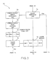
- the n-th cache unit 3n comprises an n-th common-block flag circuit 5n.
- the n-th common-block flag circuit 5n is divided into first through M-th flag bit areas FA-1, FA-2, ..., and FA-M.
- the first through the M-th flag bit areas FA-1 to FA-M correspond to first through the M-th block areas BA-1 to BA-M, respectively.
- An m-th flag bit area FA-m memorizes an m-th flag bit corresponding to an m-th memorized block, where m is variable between 1 and M, both inclusive.
- the m-th flag bit indicates presence or absence of a specific one of the memory blocks in the common memory area CMA (Fig. 2) in correspondence to the m-th memorized block.
- the n-th cache clear request CRn is supplied to an n-th cache clear circuit 6n which is connected to the common-block flag circuit 5n and to the n-th cache memory 4n. Responsive to the n-th cache clear request CRn, the n-th cache clear circuit 6n clears the n-th cache memory 4n so as to erase the m-th memorized block when the m-th flag bit indicates presence of the specific memory block in the common memory area CMA.
- the n-th fetch request FRn is supplied to an n-th block fetching circuit 7n which is connected to the main storage 20 (Fig. 1) and to the n-th cache memory 4n. Responsive to the n-th fetch request FRn, the n-th block fetching circuit 7n fetches, as a fetched block, the particular memory block from the main storage 20 when the particular memory block is absent in the n-th cache memory 4n for the n-th fetch request FRn. The n-th block fetching circuit 7n stores the fetched block in the m-th block area BA-m as the m-th memorized block. The particular memory block may or may not be one of memory blocks that is present in the common memory area CMA.
- the n-th block fetching circuit 7n is connected to an n-th common-block fetch detecting circuit 8n.
- the n-th common-block fetch detecting circuit 8n detects whether the particular memory block is present or absent in the common memory area CMA.
- the n-th common-block fetch detecting circuit 8n produces a detection signal when the particular memory block is present in the common memory area CMA.
- the n-th common-block fetch detecting circuit 8n carries out a detection operation by making a page table word include a bit which indicates whether the particular memory block is present or absent in the common memory area CMA when the multiprocessor system carries out a memory control operation by paging.
- the n-th common-block fetch detecting circuit 8n may carry out another detection operation by making the n-th fetch request FRn include a bit which indicates whether the particular memory block is present or absent in the common memory area CMA.
- the detection signal is delivered to an n-th common-block flag setting circuit 9n which is connected to the n-th common-block flag circuit 5n. Responsive to the detection signal, the n-th common-block flag setting circuit 9n sets the m-th flag bit indicative of presence of the particular memory block in the m-th flag bit area FA-m.
Landscapes
- Engineering & Computer Science (AREA)
- Theoretical Computer Science (AREA)
- Physics & Mathematics (AREA)
- General Engineering & Computer Science (AREA)
- General Physics & Mathematics (AREA)
- Memory System Of A Hierarchy Structure (AREA)
- Multi Processors (AREA)
Applications Claiming Priority (2)
| Application Number | Priority Date | Filing Date | Title |
|---|---|---|---|
| JP252906/88 | 1988-10-08 | ||
| JP63252906A JPH0769865B2 (ja) | 1988-10-08 | 1988-10-08 | 情報処理装置 |
Publications (3)
| Publication Number | Publication Date |
|---|---|
| EP0363840A2 true EP0363840A2 (de) | 1990-04-18 |
| EP0363840A3 EP0363840A3 (de) | 1991-09-11 |
| EP0363840B1 EP0363840B1 (de) | 1995-09-20 |
Family
ID=17243812
Family Applications (1)
| Application Number | Title | Priority Date | Filing Date |
|---|---|---|---|
| EP19890118583 Expired - Lifetime EP0363840B1 (de) | 1988-10-08 | 1989-10-06 | Zum wirksamen Versichern von Cache-Speicherübereinstimmung geeignete Cache-Speichereinheit |
Country Status (4)
| Country | Link |
|---|---|
| EP (1) | EP0363840B1 (de) |
| JP (1) | JPH0769865B2 (de) |
| CA (1) | CA2000180C (de) |
| DE (1) | DE68924318T2 (de) |
Cited By (1)
| Publication number | Priority date | Publication date | Assignee | Title |
|---|---|---|---|---|
| US5724549A (en) * | 1992-04-06 | 1998-03-03 | Cyrix Corporation | Cache coherency without bus master arbitration signals |
Families Citing this family (2)
| Publication number | Priority date | Publication date | Assignee | Title |
|---|---|---|---|---|
| JPH04347749A (ja) * | 1991-05-24 | 1992-12-02 | Nec Corp | 情報処理装置 |
| JP2008200806A (ja) * | 2007-02-20 | 2008-09-04 | Denso Corp | 放電加工装置 |
Family Cites Families (3)
| Publication number | Priority date | Publication date | Assignee | Title |
|---|---|---|---|---|
| JPS5073532A (de) * | 1973-10-31 | 1975-06-17 | ||
| US4410944A (en) * | 1981-03-24 | 1983-10-18 | Burroughs Corporation | Apparatus and method for maintaining cache memory integrity in a shared memory environment |
| US4785398A (en) * | 1985-12-19 | 1988-11-15 | Honeywell Bull Inc. | Virtual cache system using page level number generating CAM to access other memories for processing requests relating to a page |
-
1988
- 1988-10-08 JP JP63252906A patent/JPH0769865B2/ja not_active Expired - Lifetime
-
1989
- 1989-10-05 CA CA 2000180 patent/CA2000180C/en not_active Expired - Fee Related
- 1989-10-06 EP EP19890118583 patent/EP0363840B1/de not_active Expired - Lifetime
- 1989-10-06 DE DE1989624318 patent/DE68924318T2/de not_active Expired - Fee Related
Cited By (1)
| Publication number | Priority date | Publication date | Assignee | Title |
|---|---|---|---|---|
| US5724549A (en) * | 1992-04-06 | 1998-03-03 | Cyrix Corporation | Cache coherency without bus master arbitration signals |
Also Published As
| Publication number | Publication date |
|---|---|
| DE68924318T2 (de) | 1996-05-15 |
| JPH0769865B2 (ja) | 1995-07-31 |
| EP0363840A3 (de) | 1991-09-11 |
| CA2000180C (en) | 1996-01-30 |
| EP0363840B1 (de) | 1995-09-20 |
| CA2000180A1 (en) | 1990-04-08 |
| JPH02100741A (ja) | 1990-04-12 |
| DE68924318D1 (de) | 1995-10-26 |
Similar Documents
| Publication | Publication Date | Title |
|---|---|---|
| US4471429A (en) | Apparatus for cache clearing | |
| US5737750A (en) | Partitioned single array cache memory having first and second storage regions for storing non-branch and branch instructions | |
| EP0596636B1 (de) | Cache-Etikettenspeicher | |
| EP0042000B1 (de) | Pufferspeicher mit veränderlicher datenblocklänge | |
| TW343303B (en) | Cache flushing device and computer system applied with the same | |
| DE3688192T2 (de) | Seitenorganisierter cachespeicher mit virtueller adressierung. | |
| JP3718302B2 (ja) | 命令取り出し方法および装置 | |
| EP0482752B1 (de) | Verfahren und Vorrichtung zur Aufrechterhaltung der Integrität eines Cachespeichers | |
| RU99108446A (ru) | Архитектура интегральной микросхемы для цифровой обработки сигнала | |
| GB1182030A (en) | Data Processing Systems | |
| EP0348652A3 (de) | Prüfpunkt-Wiederholungssystem | |
| TW367441B (en) | System and method for coherency in a split-level data cache system | |
| KR970059955A (ko) | 메모리 컨트롤러 및 메모리 제어방법 | |
| US5257360A (en) | Re-configurable block length cache | |
| HK1040439B (zh) | 執行緩衝存儲部份高速操作方法及儀器 | |
| EP0363840B1 (de) | Zum wirksamen Versichern von Cache-Speicherübereinstimmung geeignete Cache-Speichereinheit | |
| CA2007167A1 (en) | Apparatus and method for increased operand availability in a data processing unit with a store through cache memory unit strategy | |
| EP0655689A2 (de) | Cachespeichesteuerungsanordung | |
| WO1995002248A1 (en) | Memory buffer having selective flush capability | |
| TW267222B (en) | Improved method and system of addressing | |
| EP0401021A3 (de) | Pufferspeicheranordnung mit Adressen zur Seitenbezeichnung und seiteninternen Adressen | |
| JPH0795307B2 (ja) | キャッシュメモリ制御回路 | |
| JP2563792B2 (ja) | 情報処理装置 | |
| JP2770383B2 (ja) | 選択呼出無線受信機 | |
| KR950005972Y1 (ko) | 다중프로세서에서 캐쉬메모리 태그 저장장치 |
Legal Events
| Date | Code | Title | Description |
|---|---|---|---|
| PUAI | Public reference made under article 153(3) epc to a published international application that has entered the european phase |
Free format text: ORIGINAL CODE: 0009012 |
|
| 17P | Request for examination filed |
Effective date: 19891102 |
|
| AK | Designated contracting states |
Kind code of ref document: A2 Designated state(s): BE DE FR GB IT NL |
|
| PUAL | Search report despatched |
Free format text: ORIGINAL CODE: 0009013 |
|
| AK | Designated contracting states |
Kind code of ref document: A3 Designated state(s): BE DE FR GB IT NL |
|
| 17Q | First examination report despatched |
Effective date: 19940309 |
|
| GRAA | (expected) grant |
Free format text: ORIGINAL CODE: 0009210 |
|
| AK | Designated contracting states |
Kind code of ref document: B1 Designated state(s): BE DE FR GB IT NL |
|
| REF | Corresponds to: |
Ref document number: 68924318 Country of ref document: DE Date of ref document: 19951026 |
|
| ITF | It: translation for a ep patent filed | ||
| ET | Fr: translation filed | ||
| PLBE | No opposition filed within time limit |
Free format text: ORIGINAL CODE: 0009261 |
|
| STAA | Information on the status of an ep patent application or granted ep patent |
Free format text: STATUS: NO OPPOSITION FILED WITHIN TIME LIMIT |
|
| 26N | No opposition filed | ||
| REG | Reference to a national code |
Ref country code: GB Ref legal event code: IF02 |
|
| PGFP | Annual fee paid to national office [announced via postgrant information from national office to epo] |
Ref country code: DE Payment date: 20060928 Year of fee payment: 18 |
|
| PGFP | Annual fee paid to national office [announced via postgrant information from national office to epo] |
Ref country code: GB Payment date: 20061004 Year of fee payment: 18 |
|
| PGFP | Annual fee paid to national office [announced via postgrant information from national office to epo] |
Ref country code: NL Payment date: 20061015 Year of fee payment: 18 |
|
| PGFP | Annual fee paid to national office [announced via postgrant information from national office to epo] |
Ref country code: IT Payment date: 20061031 Year of fee payment: 18 |
|
| PGFP | Annual fee paid to national office [announced via postgrant information from national office to epo] |
Ref country code: BE Payment date: 20061218 Year of fee payment: 18 |
|
| BERE | Be: lapsed |
Owner name: *NEC CORP. Effective date: 20071031 |
|
| GBPC | Gb: european patent ceased through non-payment of renewal fee |
Effective date: 20071006 |
|
| NLV4 | Nl: lapsed or anulled due to non-payment of the annual fee |
Effective date: 20080501 |
|
| PG25 | Lapsed in a contracting state [announced via postgrant information from national office to epo] |
Ref country code: DE Free format text: LAPSE BECAUSE OF NON-PAYMENT OF DUE FEES Effective date: 20080501 |
|
| PG25 | Lapsed in a contracting state [announced via postgrant information from national office to epo] |
Ref country code: BE Free format text: LAPSE BECAUSE OF NON-PAYMENT OF DUE FEES Effective date: 20071031 |
|
| REG | Reference to a national code |
Ref country code: FR Ref legal event code: ST Effective date: 20080630 |
|
| PG25 | Lapsed in a contracting state [announced via postgrant information from national office to epo] |
Ref country code: NL Free format text: LAPSE BECAUSE OF NON-PAYMENT OF DUE FEES Effective date: 20080501 |
|
| PGFP | Annual fee paid to national office [announced via postgrant information from national office to epo] |
Ref country code: FR Payment date: 20061010 Year of fee payment: 18 |
|
| PG25 | Lapsed in a contracting state [announced via postgrant information from national office to epo] |
Ref country code: GB Free format text: LAPSE BECAUSE OF NON-PAYMENT OF DUE FEES Effective date: 20071006 |
|
| PG25 | Lapsed in a contracting state [announced via postgrant information from national office to epo] |
Ref country code: FR Free format text: LAPSE BECAUSE OF NON-PAYMENT OF DUE FEES Effective date: 20071031 |
|
| PG25 | Lapsed in a contracting state [announced via postgrant information from national office to epo] |
Ref country code: IT Free format text: LAPSE BECAUSE OF NON-PAYMENT OF DUE FEES Effective date: 20071006 |