EP0363985B1 - Amplificateur de puissance pour circuits intégrés numériques - Google Patents
Amplificateur de puissance pour circuits intégrés numériques Download PDFInfo
- Publication number
- EP0363985B1 EP0363985B1 EP89119075A EP89119075A EP0363985B1 EP 0363985 B1 EP0363985 B1 EP 0363985B1 EP 89119075 A EP89119075 A EP 89119075A EP 89119075 A EP89119075 A EP 89119075A EP 0363985 B1 EP0363985 B1 EP 0363985B1
- Authority
- EP
- European Patent Office
- Prior art keywords
- fet
- connection
- diode
- gate
- source
- Prior art date
- Legal status (The legal status is an assumption and is not a legal conclusion. Google has not performed a legal analysis and makes no representation as to the accuracy of the status listed.)
- Expired - Lifetime
Links
Images

Classifications
-
- H—ELECTRICITY
- H03—ELECTRONIC CIRCUITRY
- H03K—PULSE TECHNIQUE
- H03K19/00—Logic circuits, i.e. having at least two inputs acting on one output; Inverting circuits
- H03K19/01—Modifications for accelerating switching
- H03K19/017—Modifications for accelerating switching in field-effect transistor circuits
- H03K19/01707—Modifications for accelerating switching in field-effect transistor circuits in asynchronous circuits
- H03K19/01721—Modifications for accelerating switching in field-effect transistor circuits in asynchronous circuits by means of a pull-up or down element
-
- H—ELECTRICITY
- H03—ELECTRONIC CIRCUITRY
- H03K—PULSE TECHNIQUE
- H03K19/00—Logic circuits, i.e. having at least two inputs acting on one output; Inverting circuits
- H03K19/003—Modifications for increasing the reliability for protection
- H03K19/00369—Modifications for compensating variations of temperature, supply voltage or other physical parameters
- H03K19/00384—Modifications for compensating variations of temperature, supply voltage or other physical parameters in field effect transistor circuits
-
- H—ELECTRICITY
- H03—ELECTRONIC CIRCUITRY
- H03K—PULSE TECHNIQUE
- H03K19/00—Logic circuits, i.e. having at least two inputs acting on one output; Inverting circuits
- H03K19/0175—Coupling arrangements; Interface arrangements
- H03K19/0185—Coupling arrangements; Interface arrangements using field effect transistors only
- H03K19/018507—Interface arrangements
- H03K19/018535—Interface arrangements of Schottky barrier type [MESFET]
-
- H—ELECTRICITY
- H03—ELECTRONIC CIRCUITRY
- H03K—PULSE TECHNIQUE
- H03K19/00—Logic circuits, i.e. having at least two inputs acting on one output; Inverting circuits
- H03K19/02—Logic circuits, i.e. having at least two inputs acting on one output; Inverting circuits using specified components
- H03K19/08—Logic circuits, i.e. having at least two inputs acting on one output; Inverting circuits using specified components using semiconductor devices
- H03K19/094—Logic circuits, i.e. having at least two inputs acting on one output; Inverting circuits using specified components using semiconductor devices using field-effect transistors
- H03K19/0952—Logic circuits, i.e. having at least two inputs acting on one output; Inverting circuits using specified components using semiconductor devices using field-effect transistors using Schottky type FET MESFET
-
- H—ELECTRICITY
- H03—ELECTRONIC CIRCUITRY
- H03K—PULSE TECHNIQUE
- H03K5/00—Manipulating of pulses not covered by one of the other main groups of this subclass
- H03K5/01—Shaping pulses
- H03K5/08—Shaping pulses by limiting; by thresholding; by slicing, i.e. combined limiting and thresholding
- H03K5/082—Shaping pulses by limiting; by thresholding; by slicing, i.e. combined limiting and thresholding with an adaptive threshold
- H03K5/086—Shaping pulses by limiting; by thresholding; by slicing, i.e. combined limiting and thresholding with an adaptive threshold generated by feedback
- H03K5/088—Shaping pulses by limiting; by thresholding; by slicing, i.e. combined limiting and thresholding with an adaptive threshold generated by feedback modified by switching, e.g. by a periodic signal or by a signal in synchronism with the transitions of the output signal
Definitions
- the present invention relates to the problem of how capacitively highly loaded lines within integrated GaAs circuits, such as those that occur in particular in the case of memory chips, can be reloaded in the shortest possible time with the aid of a suitable circuit.
- the high level should be limited to a defined value.
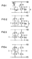
- FIG. 2 Kermano F., Takahashi K., Uetake K., Ueda K., Yamamoto R., Higashisaka A .: Fully decoded GaAs 1 kB statio RAM using closely space electrode FETs, IEEE IEDM, 1983, pages 336 to 339; Toyoda N., Kanazawa K., Terada T., Mochizuki M., Ikawa Yasuo, Hojo A .: A 256 x 4 GaAs static RAM, IEEE GaAs Symposium, 1983, pages 86 to 89) and FIG. 3 (Mead C., Conway L .: Introduction to VLSI systems. Reading: Addison Wesley, pages 17 to 18, 1980), since the gate of T32 or T33 opens in any case during a low level at the output Low level is switched. This significantly reduces the current through T32 and T33.
- T32 and T33 are NON transistors (self-conducting)
- a not negligible cross-current still flows through T32 and T42 or through T33 and T43.
- a relatively large clamping diode D2 or D3 must also be provided, which requires space and acts as an additional capacitive load.
- the circuit according to FIG. 4 (TakanoS., Tanino N., Yoshihara T., Mitsui Y., Nishitani K .: A GaAs 1-kbit static RAM with a shallow recessed-gate structure FET, IEEE Trans. Electron Devices, Vol. ED -32 (1985), 6, pages 1135 to 1139) proves to be the cheapest in terms of power consumption. However, it does not reach the full high level at the output, since the transistor T34 acts as a source follower, the source potential of which is always at least one threshold voltage below the gate potential. The gate potential of T34 cannot exceed the high level due to the gate-source diode of T24.
- the object of the present invention is to provide a circuit arrangement which enables rapid recharging and at the same time combines the low continuous current consumption of a Noff push-pull output stage with the well-defined high level of a NON-NOFF amplifier stage with an external clamping diode.
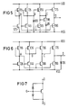
- a main problem with circuits with unswitched load elements are slow rising edges of the output signals, especially with high capacitive loads. Since the load elements are operated with a constant gate-source voltage, but the gate-source voltage of the switching transistors is switched through from zero to a maximum value, there will be increasingly flatter rising and falling edges (FIG. 8).
- the two output transistors of the push-pull stage must can be controlled by complementary signals.
- the inversion required for this is also accomplished by the Superbuffer T36, T46, T56, T66.
- the inverter T16, T26 is used to separate the still relatively large capacitive load from the previous stage. Since both the superbuffer T36, T46, T56, T66 and the pull-down transistor T86 provide a sufficiently fast falling edge, the simple inverter T16, T26 is sufficient to control them.
- the gate of the MESFET is not isolated from the channel, but is connected to it via a Schottky diode. This results in a diode effect between the gate and the other connections, as shown in FIG. 7.
- the forward voltage of these diodes determines the logic high level in a circuit, since the voltage at the input of a gate (for example inverters T16, T26 in FIG. 6) is limited by this diode.
- NOFF transistor T95 and diode D5 are used for this purpose, which means that the voltage at point C is limited to the sum of a diode forward voltage and the gate-source voltage of T95.
- the voltage will be set which corresponds to the fixed high level, since the diode is of the same type as the gate-source diode at the input of a gate.
- Transistor T95 is used to compensate for the gate-source voltage of T75. Since the transistors T75 and T95 are of the same type, gate-source voltages will arise which differ only slightly from one another. This is especially true if the ratios of the currents to the transistor dimensions of T75 and T95 match. Due to the same but weak dependency of the gate voltage on the drain current, the two gate-source voltages will still match well, even with considerable deviations in the load conditions mentioned above. In particular, fluctuations in the threshold voltages of the NOFF transistors are compensated for in this way. At the output (point D) of the amplifier, a voltage which corresponds to the level specified by the diode D5 will thus be established as a stable high level with little dependence on the current to be supplied.
- Diode D9 has the task of limiting the gate voltage of T55 and thus the current through T55, T95 and D5.
- FIG. 10 shows a power amplifier circuit with a low current consumption, a defined high level and a transient, that is to say a brief override to increase the switching speed.
- diode D5 and transistor T95 in FIG. 5 does not suddenly become conductive when a switching threshold is reached, but gradually, starting at lower voltages.
- the gradual increase in current through T95 and D5 also brakes the voltage rise at the output (point D).
- FIG. 10 shows the solution according to the invention of eliminating the influence of the limiter circuit on the rising edge.
- the negative connections (cathodes) of the diodes D10 and D20 are not statically grounded, but controlled with the help of the inverter, consisting of T100 and T110.
- the inverter consisting of T100 and T110.
- the diode D30 serves to limit the overshoot of the gate potential of T70 at high supply voltages.
Landscapes
- Engineering & Computer Science (AREA)
- Physics & Mathematics (AREA)
- Computer Hardware Design (AREA)
- Computing Systems (AREA)
- General Engineering & Computer Science (AREA)
- Mathematical Physics (AREA)
- Nonlinear Science (AREA)
- Power Engineering (AREA)
- Logic Circuits (AREA)
- Electronic Switches (AREA)
- Manipulation Of Pulses (AREA)
Claims (2)
- Circuit amplificateur numérique, dans lequel- il est prévu un premier transistor FET (T15), un second transistor FET (T25), un troisième transistor FET (T35), un quatrième transistor FET (T45), un cinquième transistor FET (T55), un sixième transistor FET (T65), un septième transistor FET (T75) et un huitième transistor FET (T85)- le premier transistor FET (T15), le troisième transistor FET (T35) et le cinquième transistor FET (T55) sont des transistors NON (autoconducteurs; normally on)- le second transistor FET (T25), le quatrième transistor FET (T45), le sixième transistor FET (T65), le septième transistor FET (T75) et le huitième transistor FET (T85) sont des transistors NOFF (autobloquants; normally off),- les bornes de drain du premier transistor FET (T15), du troisième transistor FET (T35), du cinquième transistor FET (T55) et du septième transistor FET (T75) sont reliées entre elles,- les bornes de source du second transistor FET (T25), du quatrième transistor FET (T45), du sixième transistor FET (T65) et du huitième transistor FET (T85) sont reliées entre elles,- la borne de source du premier transistor FET (T15) est raccordée à la borne de grille du premier transistor FET (T15), à la borne de drain du second transistor FET (T25), à la borne de grille du quatrième transistor FET (T45), à la borne de grille du sixième transistor FET (T65) et à la borne de grille du huitième transistor FET (T85),- la borne de source du troisième transistor FET (T35) est raccordée à la borne de grille du troisième transistor FET (T35), à la borne de drain du quatrième transistor FET (T45) et à la borne de grille du cinquième transistor FET (T55),- la borne de source du cinquième transistor FET (T55) est raccordée à la borne de drain du sixième transistor FET (T65) et à la borne de grille du septième transistor FET (T75),- la borne de source du septième transistor FET (T75) est raccordée à la borne de drain du huitième transistor FET (T85),- il est prévu un neuvième transistor FET (T95),- la borne de grille du neuvième transistor FET (T95) est raccordée à la borne de drain du sixième transistor FET (T65),- la borne de drain de ce neuvième transistor FET (T95) est raccordée à la borne de grille du septième transistor FET (T75),- il est prévu une première diode (D5) et une seconde diode (D9),- la borne de source du neuvième transistor FET (T95) est raccordée à la borne positive de la première diode (D5),- la borne de source du troisième transistor FET (T35) est raccordée à la borne positive de cette seconde diode (D9), et- les bornes négatives de la première diode (D5) et de la seconde diode (D9) sont raccordées à la borne de source du huitième transistor FET (T85).
- Circuit amplificateur numérique suivant la revendication 1, dans lequel- il est prévu une troisième diode (D30), un dixième transistor FET (T100) et un onzième transistor FET (T110),- les bornes négatives de la première diode (D5) et de la seconde diode (D9 ) sont raccordées, par l'intermédiaire de cette troisième diode (D30), à la borne de source du huitième transistor FET (T85), et la borne négative de cette troisième diode (D30) est raccordée à la borne de source du huitième transistor FET (T80),- la borne de drain du dixième transistor FET (T100) est raccordée à la borne de drain du septième transistor FET (T70),- la borne de source du dixième transistor FET (T100) est raccordée à la borne de grille du dixième transistor FET (T100), à la borne de drain du onzième transistor FET (T110) et à la borne positive de la troisième diode (D30),- la borne de source du onzième transistor FET (T110) est raccordée à la borne de source du huitième transistor FET (T80), et- la borne de grille du onzième transistor FET (T110) est raccordée à la borne de drain du huitième transistor FET (T80).
Applications Claiming Priority (2)
| Application Number | Priority Date | Filing Date | Title |
|---|---|---|---|
| DE3835119 | 1988-10-14 | ||
| DE3835119A DE3835119A1 (de) | 1988-10-14 | 1988-10-14 | Leistungsverstaerkerschaltung fuer integrierte digitalschaltungen |
Publications (3)
| Publication Number | Publication Date |
|---|---|
| EP0363985A2 EP0363985A2 (fr) | 1990-04-18 |
| EP0363985A3 EP0363985A3 (en) | 1990-08-01 |
| EP0363985B1 true EP0363985B1 (fr) | 1992-12-30 |
Family
ID=6365169
Family Applications (1)
| Application Number | Title | Priority Date | Filing Date |
|---|---|---|---|
| EP89119075A Expired - Lifetime EP0363985B1 (fr) | 1988-10-14 | 1989-10-13 | Amplificateur de puissance pour circuits intégrés numériques |
Country Status (4)
| Country | Link |
|---|---|
| US (1) | US4965464A (fr) |
| EP (1) | EP0363985B1 (fr) |
| JP (1) | JPH02149123A (fr) |
| DE (2) | DE3835119A1 (fr) |
Families Citing this family (10)
| Publication number | Priority date | Publication date | Assignee | Title |
|---|---|---|---|---|
| US5343091A (en) * | 1992-01-31 | 1994-08-30 | Kabushiki Kaisha Toshiba | Semiconductor logic integrated circuit having improved noise margin over DCFL circuits |
| JP3433359B2 (ja) * | 1993-06-18 | 2003-08-04 | 日本テキサス・インスツルメンツ株式会社 | 低電圧出力駆動回路 |
| US5453705A (en) * | 1993-12-21 | 1995-09-26 | International Business Machines Corporation | Reduced power VLSI chip and driver circuit |
| DE19547754C1 (de) * | 1995-12-20 | 1997-04-03 | Texas Instruments Deutschland | Steuerschaltung für BiCMOS-Bustreiber |
| US7969226B2 (en) * | 2009-05-07 | 2011-06-28 | Semisouth Laboratories, Inc. | High temperature gate drivers for wide bandgap semiconductor power JFETs and integrated circuits including the same |
| TWI463792B (zh) | 2009-10-29 | 2014-12-01 | Novatek Microelectronics Corp | 具有過衝抑制功能的放大電路 |
| US9837967B2 (en) | 2009-10-29 | 2017-12-05 | Novatek Microelectronics Corp. | Amplifier circuit with overshoot suppression |
| TWI715167B (zh) * | 2018-08-28 | 2021-01-01 | 美商高效電源轉換公司 | 基於GaN的高電流驅動器之故障安全停機技術 |
| TWI716980B (zh) * | 2018-08-28 | 2021-01-21 | 美商高效電源轉換公司 | 使用具回授之主動前置驅動器的GaN驅動器 |
| KR102674752B1 (ko) * | 2018-09-05 | 2024-06-14 | 이피션트 파워 컨버젼 코퍼레이션 | GaN 기반 조정 가능한 전류 드라이버 회로 |
Family Cites Families (4)
| Publication number | Priority date | Publication date | Assignee | Title |
|---|---|---|---|---|
| US4016431A (en) * | 1975-12-31 | 1977-04-05 | International Business Machines Corporation | Optimal driver for LSI |
| DE3046159A1 (de) * | 1980-12-06 | 1982-07-01 | DWK Deutsche Gesellschaft für Wiederaufarbeitung von Kernbrennstoffen mbH, 3000 Hannover | Identifizierbarer behaelter fuer radioaktive stoffe |
| DE3173257D1 (en) * | 1980-12-20 | 1986-01-30 | Itt Ind Gmbh Deutsche | Fast mos driver circuit for digital signals |
| JPS61125224A (ja) * | 1984-11-21 | 1986-06-12 | Sony Corp | 半導体回路装置 |
-
1988
- 1988-10-14 DE DE3835119A patent/DE3835119A1/de not_active Withdrawn
-
1989
- 1989-09-19 US US07/409,577 patent/US4965464A/en not_active Expired - Fee Related
- 1989-10-12 JP JP1266071A patent/JPH02149123A/ja active Pending
- 1989-10-13 EP EP89119075A patent/EP0363985B1/fr not_active Expired - Lifetime
- 1989-10-13 DE DE8989119075T patent/DE58903162D1/de not_active Expired - Fee Related
Also Published As
| Publication number | Publication date |
|---|---|
| DE58903162D1 (de) | 1993-02-11 |
| DE3835119A1 (de) | 1990-04-19 |
| EP0363985A2 (fr) | 1990-04-18 |
| US4965464A (en) | 1990-10-23 |
| JPH02149123A (ja) | 1990-06-07 |
| EP0363985A3 (en) | 1990-08-01 |
Similar Documents
| Publication | Publication Date | Title |
|---|---|---|
| DE69008075T2 (de) | CMOS-Ausgangskupplungsanordnung für Niederspannung. | |
| DE60003998T2 (de) | Bus-Treiberschaltung und Verfahren zu deren Betrieb | |
| DE69216773T2 (de) | Ausgangspufferschaltung | |
| DE69317213T2 (de) | Ausgangspufferschaltungen | |
| DE3817116A1 (de) | Ttl-kompatible ausgangs-pufferschaltung | |
| DE19946154A1 (de) | Spannungsgesteuerter Niedervolt-Oszillator mit geringer Schwankungsbreite | |
| DE2544974B2 (de) | Schaltkreis zur Realisierung logischer Funktionen | |
| EP0363985B1 (fr) | Amplificateur de puissance pour circuits intégrés numériques | |
| DE69222275T2 (de) | BICMOS-Bus-Ausgangstreiber kompatibel mit einem Mischspannungssystem | |
| DE3413139A1 (de) | Programmierte logikanordnung mit einer hilfshochzieheinrichtung zur erhoehung der vorlaufladegeschwindigkeit | |
| DE69132263T2 (de) | In einem Verbundhalbleitersubstrat gefertigter integrierter E/D Schaltkreis | |
| US4423339A (en) | Majority logic gate | |
| DE3817158A1 (de) | Integrierte, in zusammengesetzter halbleiter-technologie ausgefuehrte schaltung | |
| DE2510604A1 (de) | Integrierte digitalschaltung | |
| EP0226678B1 (fr) | Circuit logique | |
| DE3882742T2 (de) | Halbleiter - Pufferschaltung. | |
| EP0084844B1 (fr) | Circuits à transistors à effet de champ | |
| DE3237778A1 (de) | Dynamisches schieberegister | |
| DE102009008757B4 (de) | Abtastschalter mit geringem Leckverlust und Verfahren | |
| DE3817136A1 (de) | Ttl-kompatible eingangs-pufferschaltung | |
| DE3817115A1 (de) | Kondensatorgekoppelte gegentakt-logikschaltung | |
| US4661726A (en) | Utilizing a depletion mode FET operating in the triode region and a depletion mode FET operating in the saturation region | |
| DE2929383A1 (de) | Schaltungsanordnung zur spannungspegelumsetzung und zugehoeriges verfahren | |
| DE3854155T2 (de) | GaAs-Mesfet-Logik-Schaltungen mit Gegentakt-Ausgangspufferschaltungen. | |
| DE69023358T2 (de) | Logische Schaltung. |
Legal Events
| Date | Code | Title | Description |
|---|---|---|---|
| PUAI | Public reference made under article 153(3) epc to a published international application that has entered the european phase |
Free format text: ORIGINAL CODE: 0009012 |
|
| AK | Designated contracting states |
Kind code of ref document: A2 Designated state(s): DE FR GB NL |
|
| PUAL | Search report despatched |
Free format text: ORIGINAL CODE: 0009013 |
|
| AK | Designated contracting states |
Kind code of ref document: A3 Designated state(s): DE FR GB NL |
|
| 17P | Request for examination filed |
Effective date: 19900919 |
|
| 17Q | First examination report despatched |
Effective date: 19920612 |
|
| GRAA | (expected) grant |
Free format text: ORIGINAL CODE: 0009210 |
|
| AK | Designated contracting states |
Kind code of ref document: B1 Designated state(s): DE FR GB NL |
|
| REF | Corresponds to: |
Ref document number: 58903162 Country of ref document: DE Date of ref document: 19930211 |
|
| ET | Fr: translation filed | ||
| GBT | Gb: translation of ep patent filed (gb section 77(6)(a)/1977) |
Effective date: 19930305 |
|
| PG25 | Lapsed in a contracting state [announced via postgrant information from national office to epo] |
Ref country code: GB Effective date: 19931013 |
|
| PLBE | No opposition filed within time limit |
Free format text: ORIGINAL CODE: 0009261 |
|
| STAA | Information on the status of an ep patent application or granted ep patent |
Free format text: STATUS: NO OPPOSITION FILED WITHIN TIME LIMIT |
|
| 26N | No opposition filed | ||
| PG25 | Lapsed in a contracting state [announced via postgrant information from national office to epo] |
Ref country code: NL Effective date: 19940501 |
|
| GBPC | Gb: european patent ceased through non-payment of renewal fee |
Effective date: 19931013 |
|
| NLV4 | Nl: lapsed or anulled due to non-payment of the annual fee | ||
| PG25 | Lapsed in a contracting state [announced via postgrant information from national office to epo] |
Ref country code: FR Effective date: 19940630 |
|
| PG25 | Lapsed in a contracting state [announced via postgrant information from national office to epo] |
Ref country code: DE Effective date: 19940701 |
|
| REG | Reference to a national code |
Ref country code: FR Ref legal event code: ST |