EP0364038A1 - Steuerungstaktwellenform für Festkörpersbildsensoren - Google Patents
Steuerungstaktwellenform für Festkörpersbildsensoren Download PDFInfo
- Publication number
- EP0364038A1 EP0364038A1 EP89202531A EP89202531A EP0364038A1 EP 0364038 A1 EP0364038 A1 EP 0364038A1 EP 89202531 A EP89202531 A EP 89202531A EP 89202531 A EP89202531 A EP 89202531A EP 0364038 A1 EP0364038 A1 EP 0364038A1
- Authority
- EP
- European Patent Office
- Prior art keywords
- clock pulse
- sensor
- voltage
- variation
- pulse signals
- Prior art date
- Legal status (The legal status is an assumption and is not a legal conclusion. Google has not performed a legal analysis and makes no representation as to the accuracy of the status listed.)
- Withdrawn
Links
Images

Classifications
-
- G—PHYSICS
- G11—INFORMATION STORAGE
- G11C—STATIC STORES
- G11C27/00—Electric analogue stores, e.g. for storing instantaneous values
- G11C27/04—Shift registers
-
- H—ELECTRICITY
- H04—ELECTRIC COMMUNICATION TECHNIQUE
- H04N—PICTORIAL COMMUNICATION, e.g. TELEVISION
- H04N25/00—Circuitry of solid-state image sensors [SSIS]; Control thereof
- H04N25/70—SSIS architectures; Circuits associated therewith
- H04N25/76—Addressed sensors, e.g. MOS or CMOS sensors
- H04N25/7795—Circuitry for generating timing or clock signals
-
- H—ELECTRICITY
- H04—ELECTRIC COMMUNICATION TECHNIQUE
- H04N—PICTORIAL COMMUNICATION, e.g. TELEVISION
- H04N25/00—Circuitry of solid-state image sensors [SSIS]; Control thereof
- H04N25/70—SSIS architectures; Circuits associated therewith
- H04N25/71—Charge-coupled device [CCD] sensors; Charge-transfer registers specially adapted for CCD sensors
- H04N25/72—Charge-coupled device [CCD] sensors; Charge-transfer registers specially adapted for CCD sensors using frame transfer [FT]
-
- H—ELECTRICITY
- H04—ELECTRIC COMMUNICATION TECHNIQUE
- H04N—PICTORIAL COMMUNICATION, e.g. TELEVISION
- H04N25/00—Circuitry of solid-state image sensors [SSIS]; Control thereof
- H04N25/70—SSIS architectures; Circuits associated therewith
- H04N25/71—Charge-coupled device [CCD] sensors; Charge-transfer registers specially adapted for CCD sensors
- H04N25/745—Circuitry for generating timing or clock signals
Definitions
- the invention relates to a camera for television, cinematographic and/or photographic recording, including a solid-state image sensor for generating a picture signal, which sensor, controlled by clock pulse signals, operates in accordance with the accordion principle of shifting information in the sensor with an opening, a transporting and a closing phase, the opening phase involving an enlargement of picture information elements and a transport of picture information, the transporting phase involving a transport of picture information and the closing phase involving a transport of picture information and a reduction of picture information elements at the appointed locations, said sensor having a drive shift register which comprises a row of register elements outputs of which are coupled to sensor electrodes, while clock pulse inputs are coupled to the row of register elements which comprise a clock pulse-controlled series switch and a subsequent inverter circuit.
- the drive shift register for each register element comprises an NMOS transistor as a series switch and an inverter circuit comprising a PMOS and an NMOS transistor between supply terminals, while interconnected drain electrodes of these two transistors constitute the register output and are connected to the input of the subsequent register element.
- the drive shift register shifts the information in accordance with the accordion principle from an image section of the sensor to a storage section whence the picture information becomes available in a line and field-sequential manner via a parallel-in, serious-out shift register at a sensor output for the supply of the picture signal.
- a problem in the form of stripes may occur when displaying the picture signal. Horizontal stripes then occur in the line scan direction in the displayed picture. It is an object of the invention to realise a camera in which this problem of stripes is eliminated if such a problem occurs when displaying the generated picture signal.
- a camera according to the invention is characterized in that the clock pulse signals have a variation with at least three levels.
- the invention is based on the recognition that the stripe problem is caused by an incorrect transport step when shifting the information in accordance with the accordion principle.
- This incorrect transport step is related with the structure of the clock pulse signal if it has a known signal variation with two levels. Furthermore, the incorrect transport step is related with the different switching speeds for NMOS and PMOS transistors during inversion from positive to negative (from the logic 1 to 0, which is effected rapidly) and from negative to positive (from the logic 0 to 1, which is effected slowly), respectively.
- the choice of a clock pulse variation with at least three levels prevents the stripe problem when displaying the picture signal because the transport step is optimized thereby.
- the clock pulse variation with at least three levels can be realised with a staircase-shaped variation with three levels or with a sawtooth-shaped variation with a very large number of levels.
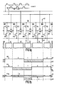
- the reference FT denotes an image sensor whose electrodes E are connected to outputs of a drive shift register SR.
- the sensor FT is, for example a frame transfer sensor, an interline sensor or a combination thereof.
- Given electrodes of the sensor electrodes E are denoted by E0, E1, E2 to E6.
- the electrodes E are shown in part and are assumed to be further extending across or in the sensor FT, insulated from the semiconductor material of the sensor.
- the part with the sensor electrodes E shown in Fig. 1a is present, for example in the storage section of the sensor FT.
- FIG. 1b shows as an example a possible charge pattern which occurs under the electrodes E in the sensor FT, dependent on the voltages which are impressed on the electrodes E.
- a positive voltage +V1 which further represents a logic 1
- a negative voltage -V1 which represents a logic 0, occurs at the electrodes E1, E2, E5 and E6.
- Fig. 1b shows the associated pattern at an instant t10. Assuming that charge packets of electrons contain picture information, they occur under the positive electrodes E0, E3 and E4, which packets are shaded in the Figure and between which barriers occur.
- a known pattern 01010101 is associated with the picture recording in the image section (not shown) of the sensor, in which case the known pattern 00110011 is associated with the transporting phase of the information shift in accordance with the accordion principle.
- a known pattern 01100110 must occur, the left-hand five values of which are shown in Fig. 1b at an instant t11i.
- the instant t11i is associated with an ideal transport step.
- Fig. 1a shows the instant t10 and t11 at two clock pulse signals Q1 and Q2 shown as a function of time t.
- the signals Q1 and Q2 shown occur in the case of a known two-phase clock pulse control of the drive shift register SR.
- Fig. 1b shows a charge pattern at the instant t11p, which pattern is produced because the barrier at the location X is not yet eliminated, whereas the greater part of the barrier at the location Y is already formed.
- the shaded charge packet spreads out, as it were, and blends with the adjacent packets. This unwanted blending leads to the stripes occurring in the line scan direction, the horizontal direction when the ultimately obtained picture signal is displayed.
- the stripe problem is caused by the combination of the information pit under the electrode E3 through which the charge spreads out, which pit is not wide and not deep enough, and by the difference in duration for the slow barrier elimination (X) and the rapid barrier formation (Y), which difference is caused by the drive shift register SR with the square wave clock pulses Q1 and Q2 shown in Fig. 1a.
- a row (SR1 ... SR6) of shift register elements SR1 to SR6 of the register SR is shown.
- Clock pulse-controlled series switches are shown as NMOS transistors N22 to N26.
- Inverter circuits are formed with PMOS transistors P11 to P15, and NMOS transistors N11 to N15. Drain electrodes of the transistors P11 ... P15, N11 ... N15 constitute the register outputs at which respective output voltages Vo1, Vo2, Vo3, Vo4 and Vo5 occur which are to be supplied to the electrodes E1 ... E5.
- N15 are connected to supply terminals conveying voltages +V1 and -V1, respectively. It will be obvious that one of the two supply terminals may be connected to ground.
- the interconnected gate electrodes of the transistors P11, N11 and so forth to P15, N15 are connected to the drain or source electrode of the preceding series switch transistor, the interconnected gate electrodes of the transistors N23 and N25, and N22, N24 and N26 receiving the clock pulse signals Q1 and Q2, respectively.
- the electrode having the highest voltage operates as a drain electrode and the electrode having the lowest voltage operates as a source electrode.
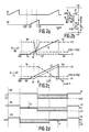
- the sawtooth-varying clock pulse signals Q1 and Q2 shown as a function of time t in Fig. 2a are used for controlling the shift register SR of Fig. 1a.
- the refernces t20, t21 and t22 denote three instants.
- the instant t20 corresponds to the instant t10 shown in Fig. 1a, which also holds true for the associated voltage patterns of Figs. 1b and 2d.
- Fig 2b shows a shift register element by means of general indications.
- the transistors P1, N1 and N2 correspond to the transistors shown in the same configuration in Fig. 1a.
- the output voltage is denoted Vo and it is applied to the electrode E shown as a capacitance.
- the input voltage is denoted Vi and is the voltage Vo of the preceding register element.
- the reference Vm denotes the voltage at the input of the inverter circuit (P2, N2).
- a clock pulse Q is applied to the gate electrode of the transistor N2.
- a gate-source threshold voltage of the transistors N1 and N2 is denoted by VTN1 and VTN2, respectively.
- Vi is smaller than Vm the electrode conveying the voltage Vi operates as a source electrode and for Vi is larger than Vm the electrode conveying the voltage Vm operates as a source electrode.
- the threshold voltage VTN1 - VTN2 is plotted as a voltage level located between the supply voltages +V1 and -V1.
- the transistor P1 of Fig. 2b being turned on and the transistors N1 and N2 being turned off.
- VTN2 gate-source threshold voltage
- Vm the voltage of the clock pulse Q
- VTN2 the gate-source threshold voltage
- Figs. 2c and 2d show that the barrier elimination at X is initiated earlier than the barrier formation at Y. With the continuous elimination there is the trailing formation.
- An optimum transport step is the result, as it shown by means of a comparison of the pattern at the instant t11p of Fig. 1b with the pattern at the instant t22 of Fig. 2d.
- the staircase-varying clock pulse signals Q1 and Q2 shown as a function of time t in Fig. 3a are used.
- the references t31 and t32 denote instants which are comparable with the instants t21 and t22 of Fig. 2a, while the instant t30 is shown at a later point of time than the instant t20.
- Fig. 3a shows the clock pulse signals having a staircase variation with three levels. What is common with the sawtooth variation shown in Fig. 2a is that the two signal variations have at least three levels.
- the sawtooth variation may be formed with a staircase variation having a large number of levels.
- the clock pulse variation shown in Fig.
- Fig. 3b shows a gate-source threshold voltage indicated by VTN2 + ⁇ V which is changed with respect to that in Fig. 2b. This change will be referred to when describing a voltage level L1 in Fig. 3c.
- Fig. 3c shows the clock pulses Q and the voltage variations Vm and Vo.
- the transporting phase at the information shift in accordance with the accordion principle has been described hereinbefore by way of example.
- the clock pulses Q with at least the three levels may be operative without any further problems and with the same advantages in the opening and closing phases in accordance with the accordion principle.
- a three-phase, four-phase or multi-phase control may be used.
Landscapes
- Engineering & Computer Science (AREA)
- Multimedia (AREA)
- Signal Processing (AREA)
- Transforming Light Signals Into Electric Signals (AREA)
Applications Claiming Priority (2)
| Application Number | Priority Date | Filing Date | Title |
|---|---|---|---|
| NL8802515 | 1988-10-13 | ||
| NL8802515 | 1988-10-13 |
Publications (1)
| Publication Number | Publication Date |
|---|---|
| EP0364038A1 true EP0364038A1 (de) | 1990-04-18 |
Family
ID=19853043
Family Applications (1)
| Application Number | Title | Priority Date | Filing Date |
|---|---|---|---|
| EP89202531A Withdrawn EP0364038A1 (de) | 1988-10-13 | 1989-10-09 | Steuerungstaktwellenform für Festkörpersbildsensoren |
Country Status (2)
| Country | Link |
|---|---|
| EP (1) | EP0364038A1 (de) |
| JP (1) | JPH02154579A (de) |
Citations (1)
| Publication number | Priority date | Publication date | Assignee | Title |
|---|---|---|---|---|
| EP0161023A1 (de) * | 1984-04-24 | 1985-11-13 | Koninklijke Philips Electronics N.V. | Ladungsgekoppelte Halbleiteranordnung mit dynamischer Steuerung |
-
1989
- 1989-10-09 EP EP89202531A patent/EP0364038A1/de not_active Withdrawn
- 1989-10-09 JP JP1263790A patent/JPH02154579A/ja active Pending
Patent Citations (1)
| Publication number | Priority date | Publication date | Assignee | Title |
|---|---|---|---|---|
| EP0161023A1 (de) * | 1984-04-24 | 1985-11-13 | Koninklijke Philips Electronics N.V. | Ladungsgekoppelte Halbleiteranordnung mit dynamischer Steuerung |
Non-Patent Citations (1)
| Title |
|---|
| SOLID-STATE ELECTRONICS, vol. 19, no. 4, April 1976, pages 279-287, Pergamon Press, GB; M.P. SINGH et al.: "Influence of clocking waveform on charge transfer in three phase charge coupled devices" * |
Also Published As
| Publication number | Publication date |
|---|---|
| JPH02154579A (ja) | 1990-06-13 |
Similar Documents
| Publication | Publication Date | Title |
|---|---|---|
| US4805026A (en) | Method for driving a CCD area image sensor in a non-interlace scanning and a structure of the CCD area image sensor for driving in the same method | |
| US4644403A (en) | Image pickup apparatus | |
| US6075565A (en) | Solid-state image sensing apparatus and its driving method | |
| JP3271086B2 (ja) | 固体撮像素子の駆動回路 | |
| EP0195270A2 (de) | Videokamera | |
| EP0506081B1 (de) | Spannungsverstärker und damit ausgerüstetes Bildaufnahmegerät | |
| EP0408025B1 (de) | Ladungsübertragungsvorrichtung und Festkörperbildaufnahmevorrichtung mit dieser Ladungsübertragungsvorrichtung | |
| AU607724B2 (en) | Charge-coupled device | |
| US5400071A (en) | Solid-state image sensing device having a multi-row direction transfer circuit | |
| EP0273486A1 (de) | CCD-Bildsensorsvorrichtung | |
| US6356305B1 (en) | Image-pickup apparatus and method for reading accumulated signal changes through transfer lines | |
| EP0621726A1 (de) | Verfahren und Gerät für eine Festkörper-Bildaufnahme-Vorrichtung | |
| EP0364038A1 (de) | Steuerungstaktwellenform für Festkörpersbildsensoren | |
| EP0161023A1 (de) | Ladungsgekoppelte Halbleiteranordnung mit dynamischer Steuerung | |
| EP0324650B1 (de) | Taktimpulsgeneratoren | |
| JP3457977B2 (ja) | シフトレジスタ | |
| US4723168A (en) | Charge-coupled device and camera comprising such a charge-coupled device | |
| US4992982A (en) | SPS type charge coupled device memory suitable for processing video information with increased speed | |
| US7623003B2 (en) | Drive method for driving element having capacity impedance, drive device, and imaging device | |
| EP0358260A1 (de) | Ansteuerschieberegister für einen Feststoffbildsensor | |
| US4868665A (en) | Charge-coupled device with varible storage capacity and constant clock frequency | |
| EP0205189A1 (de) | Elektronische Stehbildkamera | |
| JP2006115248A (ja) | クロック生成回路及び電荷結合素子駆動回路 | |
| CN120894984A (zh) | 显示面板和显示装置 | |
| US6285016B1 (en) | Scanning circuit for solid-state imaging device |
Legal Events
| Date | Code | Title | Description |
|---|---|---|---|
| PUAI | Public reference made under article 153(3) epc to a published international application that has entered the european phase |
Free format text: ORIGINAL CODE: 0009012 |
|
| AK | Designated contracting states |
Kind code of ref document: A1 Designated state(s): DE FR GB IT NL |
|
| STAA | Information on the status of an ep patent application or granted ep patent |
Free format text: STATUS: THE APPLICATION IS DEEMED TO BE WITHDRAWN |
|
| 18D | Application deemed to be withdrawn |
Effective date: 19901019 |