EP0365294A2 - Photometrisches Gerät mit einem Festkörperbildsensor - Google Patents
Photometrisches Gerät mit einem Festkörperbildsensor Download PDFInfo
- Publication number
- EP0365294A2 EP0365294A2 EP89310677A EP89310677A EP0365294A2 EP 0365294 A2 EP0365294 A2 EP 0365294A2 EP 89310677 A EP89310677 A EP 89310677A EP 89310677 A EP89310677 A EP 89310677A EP 0365294 A2 EP0365294 A2 EP 0365294A2
- Authority
- EP
- European Patent Office
- Prior art keywords
- imaging device
- solid
- state imaging
- semiconductor region
- potential level
- Prior art date
- Legal status (The legal status is an assumption and is not a legal conclusion. Google has not performed a legal analysis and makes no representation as to the accuracy of the status listed.)
- Granted
Links
- 238000003384 imaging method Methods 0.000 title claims abstract description 69
- 239000000758 substrate Substances 0.000 claims abstract description 44
- 238000005375 photometry Methods 0.000 claims description 17
- 238000000034 method Methods 0.000 claims description 10
- 238000005286 illumination Methods 0.000 claims description 3
- 239000004065 semiconductor Substances 0.000 claims 25
- 238000005036 potential barrier Methods 0.000 claims 2
- XUIMIQQOPSSXEZ-UHFFFAOYSA-N Silicon Chemical compound [Si] XUIMIQQOPSSXEZ-UHFFFAOYSA-N 0.000 description 24
- 229910052710 silicon Inorganic materials 0.000 description 24
- 239000010703 silicon Substances 0.000 description 24
- 230000035508 accumulation Effects 0.000 description 18
- 238000009825 accumulation Methods 0.000 description 18
- 238000006243 chemical reaction Methods 0.000 description 8
- 230000000694 effects Effects 0.000 description 5
- VYPSYNLAJGMNEJ-UHFFFAOYSA-N Silicium dioxide Chemical compound O=[Si]=O VYPSYNLAJGMNEJ-UHFFFAOYSA-N 0.000 description 4
- 230000000875 corresponding effect Effects 0.000 description 4
- 238000010586 diagram Methods 0.000 description 4
- GGCZERPQGJTIQP-UHFFFAOYSA-N sodium;9,10-dioxoanthracene-2-sulfonic acid Chemical compound [Na+].C1=CC=C2C(=O)C3=CC(S(=O)(=O)O)=CC=C3C(=O)C2=C1 GGCZERPQGJTIQP-UHFFFAOYSA-N 0.000 description 4
- 238000005259 measurement Methods 0.000 description 3
- 230000008569 process Effects 0.000 description 3
- 230000004044 response Effects 0.000 description 3
- 229910052681 coesite Inorganic materials 0.000 description 2
- 238000010276 construction Methods 0.000 description 2
- 229910052906 cristobalite Inorganic materials 0.000 description 2
- 238000002955 isolation Methods 0.000 description 2
- 230000015654 memory Effects 0.000 description 2
- 239000000377 silicon dioxide Substances 0.000 description 2
- 235000012239 silicon dioxide Nutrition 0.000 description 2
- 229910052682 stishovite Inorganic materials 0.000 description 2
- 229910052905 tridymite Inorganic materials 0.000 description 2
- 230000006835 compression Effects 0.000 description 1
- 238000007906 compression Methods 0.000 description 1
- 230000006870 function Effects 0.000 description 1
- 230000003287 optical effect Effects 0.000 description 1
- 238000003825 pressing Methods 0.000 description 1
- 230000009467 reduction Effects 0.000 description 1
- 239000013589 supplement Substances 0.000 description 1
Images

Classifications
-
- H—ELECTRICITY
- H04—ELECTRIC COMMUNICATION TECHNIQUE
- H04N—PICTORIAL COMMUNICATION, e.g. TELEVISION
- H04N23/00—Cameras or camera modules comprising electronic image sensors; Control thereof
- H04N23/70—Circuitry for compensating brightness variation in the scene
- H04N23/71—Circuitry for evaluating the brightness variation
-
- H—ELECTRICITY
- H04—ELECTRIC COMMUNICATION TECHNIQUE
- H04N—PICTORIAL COMMUNICATION, e.g. TELEVISION
- H04N23/00—Cameras or camera modules comprising electronic image sensors; Control thereof
- H04N23/70—Circuitry for compensating brightness variation in the scene
- H04N23/73—Circuitry for compensating brightness variation in the scene by influencing the exposure time
-
- H—ELECTRICITY
- H04—ELECTRIC COMMUNICATION TECHNIQUE
- H04N—PICTORIAL COMMUNICATION, e.g. TELEVISION
- H04N25/00—Circuitry of solid-state image sensors [SSIS]; Control thereof
- H04N25/60—Noise processing, e.g. detecting, correcting, reducing or removing noise
- H04N25/62—Detection or reduction of noise due to excess charges produced by the exposure, e.g. smear, blooming, ghost image, crosstalk or leakage between pixels
- H04N25/621—Detection or reduction of noise due to excess charges produced by the exposure, e.g. smear, blooming, ghost image, crosstalk or leakage between pixels for the control of blooming
- H04N25/622—Detection or reduction of noise due to excess charges produced by the exposure, e.g. smear, blooming, ghost image, crosstalk or leakage between pixels for the control of blooming by controlling anti-blooming drains
-
- H—ELECTRICITY
- H04—ELECTRIC COMMUNICATION TECHNIQUE
- H04N—PICTORIAL COMMUNICATION, e.g. TELEVISION
- H04N25/00—Circuitry of solid-state image sensors [SSIS]; Control thereof
- H04N25/70—SSIS architectures; Circuits associated therewith
- H04N25/703—SSIS architectures incorporating pixels for producing signals other than image signals
- H04N25/706—Pixels for exposure or ambient light measuring
-
- H—ELECTRICITY
- H10—SEMICONDUCTOR DEVICES; ELECTRIC SOLID-STATE DEVICES NOT OTHERWISE PROVIDED FOR
- H10F—INORGANIC SEMICONDUCTOR DEVICES SENSITIVE TO INFRARED RADIATION, LIGHT, ELECTROMAGNETIC RADIATION OF SHORTER WAVELENGTH OR CORPUSCULAR RADIATION
- H10F39/00—Integrated devices, or assemblies of multiple devices, comprising at least one element covered by group H10F30/00, e.g. radiation detectors comprising photodiode arrays
- H10F39/10—Integrated devices
- H10F39/12—Image sensors
- H10F39/15—Charge-coupled device [CCD] image sensors
- H10F39/153—Two-dimensional or three-dimensional array CCD image sensors
Definitions
- the present invention relates to a photometric apparatus of the type employing a solid-state imaging device provided with a vertical overflow drain.
- Various types of cameras have conventionally been available such as silver-salt still cameras of the type which record still images by using silver salt film, silver-salt movie cameras of the type which record motion images by using silver salt film, electronic still cameras of the type which record still images by using imaging devices and electronic memories such as magnetic floppy discs or the like, and video cameras of the type which record motion images by using imaging devices and magnetic tapes.
- Any of the above noted types of cameras is provided with a photometric apparatus for optimizing the amount of exposure with respect to film or the imaging device.
- the CCD is driven at the timing of photometry which is executed in response to a photographic operation and, as in a video camera for recording a motion image, during the driving of the CCD, photometry is effected while a diaphragm for exposure control is being controlled in order to supplement an insufficiency in the dynamic range thereof.
- CCD driving or diaphragm control it has been necessary that CCD driving or diaphragm control be performed not only during exposure control but at the timing of photometry.
- the time period during which the CCD is driven in one photographic cycle is long and power dissipation therefore increases. This results in a reduction in the time period during which the camera can operate with a battery supply alone.
- An exposure-amount determining system in which one viewfinder field is divided into a plurality of sections so that a proper amount of exposure is determined by metering the brightnesses of the individual sections, selecting and combining the outputs therefrom, and effecting predetermined processes such as weighting, arithmetic operations and the like.
- This exposure-amount determining system is hereinafter referred to as "multi-pattern photometric system"). If the photoconductive surface of an imaging CCD is constructed of a plurality of photoconductive segments in order to realize the multi-pattern photometric system with the imaging CCD, a signal processing circuit is needed for outputting the photometric outputs of the individual photoconductive segments at high speed. This signal processing circuit, however, increases the complexity of the entire circuit arrangement.
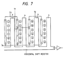
- Fig. 7 is a schematic view showing a CCD of the horizontal overflow drain type which has heretofore been commonly used, and shows a structure in which photometry is performed through the photoconductive surface of the CCD, consisting of a plurality of photoconductive segments.
- Reference numerals 71, 72, 73 and 74 denote electrode segments serving as overflow drains, and these electrode segments are employed for photometry utilizing photosensitive pixels a, b, c and d.
- an object of the present invention to provide a photometric apparatus capable of determining the amount of exposure without an increase in power dissipation.
- the substrate of a solid-state imaging device is formed as an overflow drain. More specifically, a general type of solid-state imaging device having a vertical overflow drain structure is prepared, and it is arranged so that the driving of it is completely stopped by a drive stopping means, that is, so that the imaging device is placed in a stop state in which no bias is applied. In this complete stop state, measuring means are caused to measure a photoelectric current which flows from photodiodes, each forming a photosensitive pixel, into the overflow drain in accordance with the brightness distribution of an image of an object which is focused on the photosensitive portion of the device. In addition, if an arrangement in which the amount of exposure is determined on the basis of this measurement output is adopted, automatic exposure control is enabled.
- the operation of the CCD is completely stopped at the timing of photometry with no bias applied thereto, and the photoelectric current which flows from the photosensitive portion into the overflow drain is measured. Accordingly, it is possible to effect photometry without increasing power dissipation.
- the electrode formed to cover the entire substrate surface of the solid-state imaging device be composed of a plurality of electrode segments which correspond to photometric regions into which are divided one viewfinder field. If means for measuring a photoelectric current which flows into the overflow drain while the driving of the solid-stage imaging device is being stopped is provided for each individual electrode segment, a photometric apparatus capable of multi-pattern photometry is realized with a simple device structure and without the need for critical techniques for processing fine portions.
- the photometric apparatus having the above-described construction, it is possible to arbitrarily set various photometric modes such as center-weighted metering mode for metering the brightness only at the center of a viewfinder field, average metering mode for metering the brightness over the entire viewfinder field and the like. More specifically, if the substrate electrode of the CCD is composed of isolated segments corresponding to the individual photometric regions set in the viewfinder field so that the photoelectric current which flows from each electrode segment into the overflow drain is measured, it is possible to realize a multi-pattern metering system which determines optimum photographic conditions through selection combination, weighting, arithmetic operations and the like of the measurement results.
- various photometric modes such as center-weighted metering mode for metering the brightness only at the center of a viewfinder field, average metering mode for metering the brightness over the entire viewfinder field and the like.
- Fig. 1 is a schematic view which serves to illustrate the principle of a photometric apparatus according to the present invention, showing in cross section an imaging portion and a photometric circuit of an interline-type CCD which constitutes a solid-state imaging device.
- the imaging portion of the interline-type CCD is explained with reference to Fig. 1.
- Reference numeral 1 denotes an n-type silicon substrate (n-type substrate), and an electrode 1A is formed on one surface of the n-type silicon substrate 1 (the bottom surface thereof as viewed in the figure), and a p-type region 2 is formed on the surface of the n-type silicon substrate 1 which is opposite to the aforesaid one surface.
- this p-type region 2 includes a p layer 2a and a p well 2b.
- a photoelectric-charge accumulation layer 3, which forms photosensitive pixels for photoelectric conversion, is formed on the side of the p layer 2a which is opposite to the n-type silicon substrate 1, while a vertical CCD transfer resistor 4 is formed on the side of the p well 2b which is opposite to the n-type silicon substrate 1.
- a transfer gate 8 is formed between the photoelectric-charge accumulation layer 3 and the vertical CCD transfer register 4, and a thin p-type layer 30 is formed to cover the photoelectric-charge accumulation layer 3 and the vertical CCD transfer register 4.
- An isolation layer made of SiO2 overlies the photoelectric-charge accumulation layer 3 and the vertical CCD transfer register 4.
- a transfer register electrode 5 is formed in the portion of the SiO2 isolation layer which corresponds to the vertical CCD transfer register 4, and a light shielding layer 9 is formed to cover the vertical CCD transfer register 4 and the transfer gate 8.
- a current-to-voltage conversion amplifier 7 is provided as a photometric circuit section which is suitably used in combination with the imaging section of the above-described interline-type CCD having the above-described structure.
- the p-type region 2 is connected to one of the input terminals of the current-to-voltage conversion amplifier 7.
- the electrode 1A formed on the n-type silicon substrate 1 is selectively connected to the other input terminal of the current-to-voltage conversion amplifier 7 or a bias supply V SUB by means of a selecting switch 6.
- the selecting switch 6 is switched to a side connected to the bias supply V SUB to apply a bias voltage V SUB to the substrate 1. During this time, drive pulses for transfer purposes are being applied to the transfer register electrode 5 of the vertical CCD transfer register 4.
- Fig. 2 shows a potential distribution appearing while the interline-type CCD of Fig. 1 is being driven.
- the potential distribution of Fig. 2 which appears while the interline-type CCD is being driven, if signal charges, which are generated in the photoelectric-charge accumulation layer 3 by illumination from the outside, pass through the p layer 2a in the p-type region 2, then the signal charges flow into the bias supply V SUB which is applying a bias voltage to the electrode 1A of the n-type silicon substrate 1, but they do not enter the vertical CCD transfer register 4. Accordingly, so-called blooming does not take place.
- the n-type silicon substrate 1 the structure of which has a potential distribution such as that shown in Fig. 2 is hereinafter referred to as a vertical overflow drain (OFD). While such an n-type silicon substrate 1, that is, an interline-type CCD the substrate of which forms a vertical overflow drain, is being driven, the maximum number of electric charges to be accumulated in the photoelectric-charge accumulation layer 3 is limited. It follows, therefore, that the interline-type CCD including the vertical overflow drain has a limited dynamic range, within which the amount of exposure is determined by transferring the charges generated in the photoelectric-charge accumulation layer 3 to the outside through the vertical CCD transfer register 4.
- the photoelectric charges are not read into the vertical CCD transfer register 4, they overflows from the photoelectric-charge accumulation layer 3 to form a photoelectric current which flows into the n-type silicon substrate 1 the overflow drain.
- Such an overflow occurs in all the photosensitive pixels the photoelectric-charge accumulation layer 3.
- the amount of electric current which flows into the overflow drain is proportional to the quantity of light received by the photosensitive pixels.
- the electric current which flows into the overflow drain while the bias voltage V SUB is being applied to the n-type silicon substrate 1 includes a large amount of dark current which is generated in a deep portion of the p-type region 2. For this reason, it is in effect difficult to measure the infinitesimal photoelectric current which flows out of the photoelectric-charge accumulation layer 3.
- the bias voltage V SUB is not being applied to the n-type silicon substrate 1, no dark current, which flows into the overflow drain, is generated. Accordingly, in a non-biased state, it is possible to measure the photoelectric current 4 which flows from the photoelectric-charge accumulation layer 3.
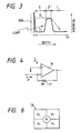
- Fig. 3 is a graphic representation which shows the potential distribution measured along the depth in a conduction band immediately below the photoelectric-charge accumulation layer 3 when driving of the solid-state imaging device the interline-type CCD, is stopped and the bias is set to zero.
- Ef denotes a Felmi level in an equilibrium state wherein no light is externally incident. In a light-shielded state, the photoelectric-charge accumulation layer 3 is empty and therefore assumes the state of potential I shown in Fig. 3.
- Fig. 4 is a circuit diagram which serves to illustrate the principle of the current-to-voltage conversion amplifier 7 shown in Fig. 1.
- This amplifier 7 is arranged to detect a photoelectric current which overflows into the n-type silicon substrate 1 during the complete stop state of the interline-type CCD shown in Fig. 3, that is to say, when the driving of the vertical CCD transfer register 4 is stopped and no bias is applied.
- the input impedance takes on a value obtained by dividing the resistance Rf of a feedback resistor 11 by the release voltage gain.
- the input impedance can be rendered an extremely small value so that it can be considered that the short current between the p-type region 2 and the n-type silicon substrate 1 is approximately measured.
- the electrode 1A for biasing the vertical overflow drain of the ordinary interline-type CCD is formed to cover the entire surface of the n-type silicon substrate 1 which constitutes the reverse surface of the CCD device. Accordingly, uniform bias is applied to the overall imaging surface of the CCD device.
- the electrode 1A of the n-type silicon substrate 1 is composed of a plurality of electrode segments and the photoelectric current of each electrode segment is measured with the current-to-voltage conversion amplifier 7 shown in Fig. 4.
- the input impedance of the current-to-voltage conversion amplifier 7 is sufficiently small, a major portion of the photoelectric charges generated in one pixel a single photoelectric-charge accumulation layer 3, flows into the overflow drain electrode immediately below it. It is to be understood, therefore, that the number of photoelectric charges which diffuse in the horizontal direction is relatively small.
- the photoelectric current corresponding to each electrode segment, which flows into the overflow drain, directly reflects the two-dimensional pattern of light incident upon the imaging surface of the CCD device.
- the electrode segments of the electrode 1A formed on the surface of the n-type silicon substrate 1 which corresponds to the reverse surface of the CCD device are each formed into an arbitrary configuration so that the outputs from the individual electrode segments are weighted or subjected to appropriate arithmetic operations, it becomes possible to readily set various types of photometric modes such as, for example, a center-weighted metering mode, a periphery-weighted metering mode, an average metering mode, and a multi-pattern metering mode (one kind of photometric system in which one viewfinder field is divided into a plurality of regions so that the outputs from the individual regions are computed to obtain a proper exposure value).
- a center-weighted metering mode such as, for example, a center-weighted metering mode, a periphery-weighted metering mode, an average metering mode, and a multi-pattern metering mode (one kind of photometric system in which one viewfinder field is
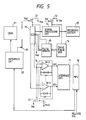
- Fig. 5 is a circuit block diagram which serves to illustrate one embodiment of the present invention based on the photometric principle shown in Figs. 1 to 4.
- An image of an object is focused on a solid-state imaging device 12 through a photographic lens 21 and a shutter 19.
- the solid-state imaging device 12 is driven by a drive-pulse generator 14 and a pulse driver 15.
- Photoelectric charges, which are accumulated in the photoelectric-charge accumulation layer the photosensitive pixels, throughout the exposure time determine by the release period of the shutter 19, are output as a signal, corresponding to the generated photoelectric charges, in response to vertical transfer driving and horizontal transfer driving exerted by a pulse driver 15.
- the output from the solid-state imaging device 12 is converted into a predetermined video signal in a signal processing circuit 13, and the signal thus converted is transferred to a recording system 25, where it is recorded on a disc, a memory or the like as still-image data for one frame.
- the solid-state imaging device 12 has the structure shown in Fig. 1, and the p-type region 2 is fixed to a predetermined potential V SS .
- the electrode 1A of the n-type silicon substrate 1 shown in Fig. 1 the overflow drain electrode, consists of n electrode segments. These n electrode segments are respectively connected to photometric amplifiers 16-1, ..., 16-n provided in a photometric circuit 16. These photometric amplifiers 16-1, ..., 16-n are arranged to effect current-to-voltage conversion as well as logarithmic compression.
- Outputs Vp1 to Vpn from the photometric amplifiers 16-1 to 16-n are input to a microprocessor (MPU) 18 over an interface circuit 17.
- MPU microprocessor
- the solid-state imaging device 12 is provided with a selecting switch 22 for effecting switching between an electrical source V DD and the predetermined potential V SS .
- the signal processing circuit 13 is provided with a switch 23 for effecting switching between an electrical source V CC and the predetermined potential V SS .
- a selecting switch 24 is provided for effecting switching between the bias source V SUB and the predetermined potential V SS .
- the microprocessor 18 is arranged to receive a release signal issued in response to the operation of pressing a shutter release button, and also to provide control over the shutter 19 and aperture control over the photographic lens 21 through the interface circuit 20.
- the switches 22 and 23 are switched to the respective V SS sides to stop the driving of the solid-state imaging device 12.
- the switch 24 is switched to the V SS side to place the solid-state imaging device 12 in a non-biased state.
- electrical currents flowing from the individual overflow-drain electrode segments of the solid-state imaging device 12 are measured by the corresponding photometric amplifiers 16-1 to 16-n.
- the microprocessor 18 sequentially reads the measurement output voltages Vp1 to Vpn through the interface circuit 17 and stores them in a RAM or the like on the microprocessor 18.
- the shutter 19 is open under the control of the processor 18 through the interface circuit 20.
- the microprocessor 18 temporarily closes the shutter 16.
- the switches 22, 23 and 24 are switched to the V DD side, the V CC side and the bias-supply V SUB side, respectively, and the solid-state imaging device 12, the signal processing circuit 13 and the recording system 25 are each placed in an operative state.
- the microprocessor 18 carries out aperture control of the photographing lens 21 and drives the shutter 19 in accordance with the aperture value and the shutter speed both of which are required to assure the amount of exposure determined by the photometric value previously obtained from the photometric circuit 16.
- the microprocessor 18 reads from the solid-state imaging device 12 a signal output which represents the number of photoelectric charges accumulated in accordance with the brightness of the object to be photographed, and causes the signal processing circuit 13 to apply predetermined signal processing to the read signal output, thereby converting it into a video signal.
- This video signal is delivered to the recording system 25, where still-image data for one frame is recorded.
- Fig. 6 is a schematic view showing an example of the overflow drain electrode of the solid-state imaging device of Fig. 5.
- the electrode 1A which is formed to cover the entire surface of the n-type silicon substrate 1 which constitutes the reverse surface of the CCD device as shown in Fig. 1, consists of five electrode segments P1 to P5.
- the central electrode segment P1 has an approximately circular configuration and the neighboring four electrode segments P2 to P5 each have an approximately rectangular configuration.
- the amount of exposure may be determined on the basis of the photometric result obtained from the center electrode segment P1. If the average metering mode is selected, the photometric outputs from all the electrode segments P1 to P5 may be utilized.
- Fig. 5 employs a mechanical shutter
- the shutter a solid-state imaging device capable of purely electronically realizing a shutter function. If such an imaging device is employed, the shutter 19, hence the shutter control, can be omitted.
- the photometric apparatus since photometry is performed by using the solid-state imaging device for imaging purposes, a separate photometric sensor or a separate optical system is not needed.
- the solid-state imaging device for imaging purposes is being used for photometric purposes, the driving of the solid-state imaging device itself is completely stopped and the signal processing circuit itself does not operate.
- the photometric apparatus according to the present invention can effect photometry with an extremely small amount of power dissipation and, although the solid-state image device for imaging purposes is utilized for photometry, there is no risk of reducing the operational life of batteries.
- the vertical overflow drain electrode consists of electrode segments, it is possible to readily realize multi-pattern photometry with a simple structure and without the need for critical techniques for processing extremely fine portions.
Landscapes
- Engineering & Computer Science (AREA)
- Multimedia (AREA)
- Signal Processing (AREA)
- Transforming Light Signals Into Electric Signals (AREA)
- Solid State Image Pick-Up Elements (AREA)
- Light Receiving Elements (AREA)
- Photometry And Measurement Of Optical Pulse Characteristics (AREA)
Applications Claiming Priority (2)
| Application Number | Priority Date | Filing Date | Title |
|---|---|---|---|
| JP262367/88 | 1988-10-18 | ||
| JP63262367A JP2720478B2 (ja) | 1988-10-18 | 1988-10-18 | 縦型オーバーフロードレインを備える固体撮像素子を用いた測光装置 |
Publications (3)
| Publication Number | Publication Date |
|---|---|
| EP0365294A2 true EP0365294A2 (de) | 1990-04-25 |
| EP0365294A3 EP0365294A3 (de) | 1991-05-02 |
| EP0365294B1 EP0365294B1 (de) | 1996-08-21 |
Family
ID=17374759
Family Applications (1)
| Application Number | Title | Priority Date | Filing Date |
|---|---|---|---|
| EP89310677A Expired - Lifetime EP0365294B1 (de) | 1988-10-18 | 1989-10-18 | Photometrisches Gerät mit einem Festkörperbildsensor |
Country Status (4)
| Country | Link |
|---|---|
| US (1) | US4977312A (de) |
| EP (1) | EP0365294B1 (de) |
| JP (1) | JP2720478B2 (de) |
| DE (1) | DE68926990T2 (de) |
Cited By (6)
| Publication number | Priority date | Publication date | Assignee | Title |
|---|---|---|---|---|
| DE4133996A1 (de) * | 1990-10-13 | 1992-04-16 | Gold Star Electronics | Ccd-bildwandler |
| WO1992010854A1 (en) * | 1990-12-12 | 1992-06-25 | Eastman Kodak Company | Image device with photodiode having real time readout property |
| WO1992022091A1 (en) * | 1991-06-07 | 1992-12-10 | Eastman Kodak Company | Enhanced exposure latitude of image sensor having lateral overflow drain |
| EP0630152A3 (de) * | 1993-06-18 | 1995-07-05 | Canon Kk | Photoelektrischer Umwandler. |
| WO1996034416A1 (en) * | 1995-04-28 | 1996-10-31 | Sunnybrook Hospital | Active matrix x-ray imaging array |
| WO2007035860A2 (en) | 2005-09-21 | 2007-03-29 | Rjs Technology, Inc. | System and method for image sensor element or array with photometric and realtime reporting capabilities |
Families Citing this family (8)
| Publication number | Priority date | Publication date | Assignee | Title |
|---|---|---|---|---|
| DE69108803T2 (de) * | 1990-01-08 | 1995-08-24 | Nippon Kogaku Kk | Anordnung für die Verarbeitung von Stehbildern. |
| JP2000092395A (ja) * | 1998-09-11 | 2000-03-31 | Nec Corp | 固体撮像装置およびその駆動方法 |
| JP4695902B2 (ja) * | 2005-03-18 | 2011-06-08 | キヤノン株式会社 | 固体撮像装置の製造方法 |
| JP5125010B2 (ja) * | 2006-07-20 | 2013-01-23 | ソニー株式会社 | 固体撮像装置、及び制御システム |
| US8184188B2 (en) * | 2009-03-12 | 2012-05-22 | Micron Technology, Inc. | Methods and apparatus for high dynamic operation of a pixel cell |
| JP5446738B2 (ja) * | 2009-11-02 | 2014-03-19 | ソニー株式会社 | 固体撮像素子およびカメラシステム |
| CN113063996A (zh) * | 2016-04-28 | 2021-07-02 | 中国科学院空天信息创新研究院 | 一种静电驱动金属微结构电场传感器 |
| CN106093605A (zh) * | 2016-06-08 | 2016-11-09 | 中国科学院电子学研究所 | 一种扭转式电场传感器 |
Family Cites Families (5)
| Publication number | Priority date | Publication date | Assignee | Title |
|---|---|---|---|---|
| US3934161A (en) * | 1974-04-29 | 1976-01-20 | Texas Instruments Incorporated | Electronic shutter for a charge-coupled imager |
| US4527182A (en) * | 1980-09-19 | 1985-07-02 | Nippon Electric Co., Ltd. | Semiconductor photoelectric converter making excessive charges flow vertically |
| JPS6020687A (ja) * | 1983-07-15 | 1985-02-01 | Nippon Kogaku Kk <Nikon> | 電子スチルカメラ |
| DE3706252A1 (de) * | 1986-02-28 | 1987-09-03 | Canon Kk | Halbleiterfotosensor |
| US4879470A (en) * | 1987-01-16 | 1989-11-07 | Canon Kabushiki Kaisha | Photoelectric converting apparatus having carrier eliminating means |
-
1988
- 1988-10-18 JP JP63262367A patent/JP2720478B2/ja not_active Expired - Lifetime
-
1989
- 1989-10-10 US US07/419,116 patent/US4977312A/en not_active Expired - Lifetime
- 1989-10-18 DE DE68926990T patent/DE68926990T2/de not_active Expired - Lifetime
- 1989-10-18 EP EP89310677A patent/EP0365294B1/de not_active Expired - Lifetime
Cited By (12)
| Publication number | Priority date | Publication date | Assignee | Title |
|---|---|---|---|---|
| DE4133996A1 (de) * | 1990-10-13 | 1992-04-16 | Gold Star Electronics | Ccd-bildwandler |
| WO1992010854A1 (en) * | 1990-12-12 | 1992-06-25 | Eastman Kodak Company | Image device with photodiode having real time readout property |
| WO1992022091A1 (en) * | 1991-06-07 | 1992-12-10 | Eastman Kodak Company | Enhanced exposure latitude of image sensor having lateral overflow drain |
| EP0630152A3 (de) * | 1993-06-18 | 1995-07-05 | Canon Kk | Photoelektrischer Umwandler. |
| US5663555A (en) * | 1993-06-18 | 1997-09-02 | Canon Kabushiki Kaisha | Photo-electric converter with parallel connection elements and dual signal read out means |
| WO1996034416A1 (en) * | 1995-04-28 | 1996-10-31 | Sunnybrook Hospital | Active matrix x-ray imaging array |
| US5962856A (en) * | 1995-04-28 | 1999-10-05 | Sunnybrook Hospital | Active matrix X-ray imaging array |
| WO2007035860A2 (en) | 2005-09-21 | 2007-03-29 | Rjs Technology, Inc. | System and method for image sensor element or array with photometric and realtime reporting capabilities |
| EP1938060A4 (de) * | 2005-09-21 | 2009-09-30 | Rjs Technology Inc | System und verfahren für ein bildsensorelement oder -array mit fotometrischen und echtzeit-meldefähigkeiten |
| US7782369B2 (en) | 2005-09-21 | 2010-08-24 | Rjs Technology, Inc. | System and method for a high dynamic range sensitive sensor element or array with gain control |
| US7786422B2 (en) | 2005-09-21 | 2010-08-31 | Rjs Technology, Inc. | System and method for a high dynamic range sensitive sensor element or array |
| US7800669B2 (en) | 2005-09-21 | 2010-09-21 | R.J.S. Technology, Inc. | System and method for image sensor element or array with photometric and realtime reporting capabilities |
Also Published As
| Publication number | Publication date |
|---|---|
| DE68926990D1 (de) | 1996-09-26 |
| EP0365294A3 (de) | 1991-05-02 |
| JP2720478B2 (ja) | 1998-03-04 |
| US4977312A (en) | 1990-12-11 |
| DE68926990T2 (de) | 1997-01-16 |
| JPH02108924A (ja) | 1990-04-20 |
| EP0365294B1 (de) | 1996-08-21 |
Similar Documents
| Publication | Publication Date | Title |
|---|---|---|
| US4977312A (en) | Photometric apparatus employing solid-state imaging device | |
| TWI552601B (zh) | 用於影像感測器之曝光控制 | |
| EP0280511B1 (de) | Stehbildvideokamera | |
| JP4846159B2 (ja) | 自動露出検出をする高感度貯蔵画素センサー | |
| US6046466A (en) | Solid-state imaging device | |
| US4338514A (en) | Apparatus for controlling exposure of a solid state image sensor array | |
| JPH07114474B2 (ja) | 電子スチルカメラ | |
| JPH07114472B2 (ja) | 固体撮像素子の駆動方法 | |
| JPH0432589B2 (de) | ||
| JPS63110877A (ja) | 電子スチルカメラ | |
| JPH0235514B2 (de) | ||
| JPH0399589A (ja) | 固体カメラ | |
| JPH077677A (ja) | 光電変換装置 | |
| JPS62243483A (ja) | 撮像装置 | |
| US4591917A (en) | Solid state image sensor | |
| US20020030151A1 (en) | Method and apparatus for instantaneous exposure control in digital imaging devices | |
| JP2987454B2 (ja) | 撮像装置 | |
| JPH0316831B2 (de) | ||
| JP3147952B2 (ja) | 測光装置 | |
| JPS60183880A (ja) | 固体撮像素子 | |
| JPH10257382A (ja) | 電子カメラ | |
| JPS58154976A (ja) | 固体撮像素子 | |
| JPH02134986A (ja) | 撮像装置 | |
| JPS6350172A (ja) | ビデオカメラ装置 | |
| JP2802946B2 (ja) | スチルビデオカメラ |
Legal Events
| Date | Code | Title | Description |
|---|---|---|---|
| PUAI | Public reference made under article 153(3) epc to a published international application that has entered the european phase |
Free format text: ORIGINAL CODE: 0009012 |
|
| AK | Designated contracting states |
Kind code of ref document: A2 Designated state(s): DE FR GB |
|
| RIN1 | Information on inventor provided before grant (corrected) |
Inventor name: JUEN, MASAHIRO 602 GURINPURAZA MUTSUURA |
|
| PUAL | Search report despatched |
Free format text: ORIGINAL CODE: 0009013 |
|
| AK | Designated contracting states |
Kind code of ref document: A3 Designated state(s): DE FR GB |
|
| 17P | Request for examination filed |
Effective date: 19910731 |
|
| 17Q | First examination report despatched |
Effective date: 19940208 |
|
| GRAH | Despatch of communication of intention to grant a patent |
Free format text: ORIGINAL CODE: EPIDOS IGRA |
|
| GRAH | Despatch of communication of intention to grant a patent |
Free format text: ORIGINAL CODE: EPIDOS IGRA |
|
| GRAA | (expected) grant |
Free format text: ORIGINAL CODE: 0009210 |
|
| AK | Designated contracting states |
Kind code of ref document: B1 Designated state(s): DE FR GB |
|
| REF | Corresponds to: |
Ref document number: 68926990 Country of ref document: DE Date of ref document: 19960926 |
|
| ET | Fr: translation filed | ||
| PLBE | No opposition filed within time limit |
Free format text: ORIGINAL CODE: 0009261 |
|
| STAA | Information on the status of an ep patent application or granted ep patent |
Free format text: STATUS: NO OPPOSITION FILED WITHIN TIME LIMIT |
|
| 26N | No opposition filed | ||
| REG | Reference to a national code |
Ref country code: GB Ref legal event code: IF02 |
|
| PGFP | Annual fee paid to national office [announced via postgrant information from national office to epo] |
Ref country code: DE Payment date: 20081016 Year of fee payment: 20 |
|
| PGFP | Annual fee paid to national office [announced via postgrant information from national office to epo] |
Ref country code: FR Payment date: 20081014 Year of fee payment: 20 |
|
| PGFP | Annual fee paid to national office [announced via postgrant information from national office to epo] |
Ref country code: GB Payment date: 20081015 Year of fee payment: 20 |
|
| REG | Reference to a national code |
Ref country code: GB Ref legal event code: PE20 Expiry date: 20091017 |
|
| PG25 | Lapsed in a contracting state [announced via postgrant information from national office to epo] |
Ref country code: GB Free format text: LAPSE BECAUSE OF EXPIRATION OF PROTECTION Effective date: 20091017 |