EP0365785A2 - Bancs de filtres pour le multiplexage/démultiplexage en fréquence de canaux de signaux. - Google Patents
Bancs de filtres pour le multiplexage/démultiplexage en fréquence de canaux de signaux. Download PDFInfo
- Publication number
- EP0365785A2 EP0365785A2 EP89115677A EP89115677A EP0365785A2 EP 0365785 A2 EP0365785 A2 EP 0365785A2 EP 89115677 A EP89115677 A EP 89115677A EP 89115677 A EP89115677 A EP 89115677A EP 0365785 A2 EP0365785 A2 EP 0365785A2
- Authority
- EP
- European Patent Office
- Prior art keywords
- complex
- filters
- filter
- cascade
- valued
- Prior art date
- Legal status (The legal status is an assumption and is not a legal conclusion. Google has not performed a legal analysis and makes no representation as to the accuracy of the status listed.)
- Granted
Links
- 238000005070 sampling Methods 0.000 claims abstract description 20
- 230000010355 oscillation Effects 0.000 claims abstract description 5
- 230000004044 response Effects 0.000 claims abstract description 4
- 238000013461 design Methods 0.000 abstract description 4
- 238000004519 manufacturing process Methods 0.000 abstract description 2
- 238000012360 testing method Methods 0.000 abstract description 2
- 238000007792 addition Methods 0.000 description 9
- 238000001228 spectrum Methods 0.000 description 7
- 238000012546 transfer Methods 0.000 description 6
- 230000008901 benefit Effects 0.000 description 5
- 238000010586 diagram Methods 0.000 description 4
- 230000009467 reduction Effects 0.000 description 3
- 230000005540 biological transmission Effects 0.000 description 2
- 230000003595 spectral effect Effects 0.000 description 2
- 230000007704 transition Effects 0.000 description 2
- 238000013459 approach Methods 0.000 description 1
- 230000000712 assembly Effects 0.000 description 1
- 238000000429 assembly Methods 0.000 description 1
- 230000000903 blocking effect Effects 0.000 description 1
- 230000008859 change Effects 0.000 description 1
- 230000000694 effects Effects 0.000 description 1
- 238000012545 processing Methods 0.000 description 1
Images


Classifications
-
- H—ELECTRICITY
- H03—ELECTRONIC CIRCUITRY
- H03H—IMPEDANCE NETWORKS, e.g. RESONANT CIRCUITS; RESONATORS
- H03H17/00—Networks using digital techniques
- H03H17/02—Frequency selective networks
- H03H17/0248—Filters characterised by a particular frequency response or filtering method
- H03H17/0264—Filter sets with mutual related characteristics
- H03H17/0273—Polyphase filters
- H03H17/0275—Polyphase filters comprising non-recursive filters
- H03H17/0276—Polyphase filters comprising non-recursive filters having two phases
-
- H—ELECTRICITY
- H03—ELECTRONIC CIRCUITRY
- H03H—IMPEDANCE NETWORKS, e.g. RESONANT CIRCUITS; RESONATORS
- H03H17/00—Networks using digital techniques
- H03H17/02—Frequency selective networks
- H03H17/0248—Filters characterised by a particular frequency response or filtering method
- H03H17/0264—Filter sets with mutual related characteristics
- H03H17/0266—Filter banks
-
- H—ELECTRICITY
- H03—ELECTRONIC CIRCUITRY
- H03H—IMPEDANCE NETWORKS, e.g. RESONANT CIRCUITS; RESONATORS
- H03H17/00—Networks using digital techniques
- H03H17/02—Frequency selective networks
- H03H17/06—Non-recursive filters
- H03H17/0621—Non-recursive filters with input-sampling frequency and output-delivery frequency which differ, e.g. extrapolation; Anti-aliasing
- H03H17/0635—Non-recursive filters with input-sampling frequency and output-delivery frequency which differ, e.g. extrapolation; Anti-aliasing characterized by the ratio between the input-sampling and output-delivery frequencies
- H03H17/065—Non-recursive filters with input-sampling frequency and output-delivery frequency which differ, e.g. extrapolation; Anti-aliasing characterized by the ratio between the input-sampling and output-delivery frequencies the ratio being integer
- H03H17/0657—Non-recursive filters with input-sampling frequency and output-delivery frequency which differ, e.g. extrapolation; Anti-aliasing characterized by the ratio between the input-sampling and output-delivery frequencies the ratio being integer where the output-delivery frequency is higher than the input sampling frequency, i.e. interpolation
-
- H—ELECTRICITY
- H03—ELECTRONIC CIRCUITRY
- H03H—IMPEDANCE NETWORKS, e.g. RESONANT CIRCUITS; RESONATORS
- H03H17/00—Networks using digital techniques
- H03H17/02—Frequency selective networks
- H03H17/06—Non-recursive filters
- H03H17/0621—Non-recursive filters with input-sampling frequency and output-delivery frequency which differ, e.g. extrapolation; Anti-aliasing
- H03H17/0635—Non-recursive filters with input-sampling frequency and output-delivery frequency which differ, e.g. extrapolation; Anti-aliasing characterized by the ratio between the input-sampling and output-delivery frequencies
- H03H17/065—Non-recursive filters with input-sampling frequency and output-delivery frequency which differ, e.g. extrapolation; Anti-aliasing characterized by the ratio between the input-sampling and output-delivery frequencies the ratio being integer
- H03H17/0664—Non-recursive filters with input-sampling frequency and output-delivery frequency which differ, e.g. extrapolation; Anti-aliasing characterized by the ratio between the input-sampling and output-delivery frequencies the ratio being integer where the output-delivery frequency is lower than the input sampling frequency, i.e. decimation
-
- H—ELECTRICITY
- H04—ELECTRIC COMMUNICATION TECHNIQUE
- H04J—MULTIPLEX COMMUNICATION
- H04J4/00—Combined time-division and frequency-division multiplex systems
- H04J4/005—Transmultiplexing
-
- H—ELECTRICITY
- H03—ELECTRONIC CIRCUITRY
- H03H—IMPEDANCE NETWORKS, e.g. RESONANT CIRCUITS; RESONATORS
- H03H2218/00—Indexing scheme relating to details of digital filters
- H03H2218/04—In-phase and quadrature [I/Q] signals
Definitions
- the invention relates to a filter bank according to the preamble of claims 1 or 2.
- Fitter banks are known, for example from the article by Del Re and Emiliani "An Analytical Signal Approach for Transmultiplexers: Theory and Design" in IEEE Transactions on Communications, Vol. Com-30, No.7, July 1982, pages 1623 ff.
- Such filter banks are mainly used for multiplexing or demultiplexing individual FDM channels in so-called transmultiplexers, which are used to convert FDM to TDM or vice versa and are used, for example, in satellite technology or in the telephone network.
- transmultiplexers which are used to convert FDM to TDM or vice versa and are used, for example, in satellite technology or in the telephone network.
- the top priority is to ensure that the payload is as low as possible.
- the present invention was therefore based on the object of specifying a filter bank of the type mentioned at the outset in which the circuit complexity is reduced still further or in which even further improved system properties can be achieved with unchanged circuit complexity.
- the filter bank according to the invention has the advantage of a smaller circuit complexity or the advantage of better system properties with the same circuit complexity.
- Advantageous embodiments of the invention result from the subclaims.
- the advantage of the present filter bank has the effect that the number of filters with different coefficients is greatly reduced. In optimal cases, this is designed so that all cascaded filters one
- One-way transmultiplexer channel that is to say of a branch, although they have different coefficients, but in the individual cascade stages an identical filter with identical coefficients can be used for all channels. Furthermore, the coefficients of these filters are real, which greatly reduces the number of computing operations.
- the computational effort can be reduced by making the more complex filters of the latter cascade levels the same for all channels within a cascade level.
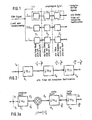
- FIGS 1 and 2 show the block diagram of an FDM demultiplexer according to the solution after the main application.
- FIGS 3a and 3b each show an embodiment according to the present invention.
- FIGS. 5 and 6 show detailed block diagrams for the multiplier used for complex-value factors and for a half-band filter with real coefficient ends.
- FIG. 7 shows a detailed circuit diagram of a branch of a half-band filter.
- FIG. 8 shows a filter cascade as an example, on the basis of which the reduced switching or multiplication and addition effort is calculated.
- the FDM input signal can be real or complex.
- the coefficients of the individual filters are different across the channel or across the cascade level.
- FIG. 2 shows more details for a single cascade branch of the demultiplexer according to FIG. 1, also according to the status of the main application.
- the sampling rate, on the input side f A is reduced by a factor of 2.
- FIGS. 3a and 3b show the design of a filter bank according to the invention. According to Figure 3a after the first filter. with the transfer function H l1, a multiplier is inserted, which outputs the complex-value output signals S 2 with the samples of a complex carrier oscillation e -j2 ⁇ k. / multiplied.
- k is the discrete time variable, the channel band center frequency in the area of the first cascade stage I and the sampling rate at the same point in question.
- the complex output signal S 2 is now fed to the next filter of the following cascade stage, the transfer function being H 12 .
- FIG. 4a shows the transfer function
- is also plotted in the transmission range.
- the demultiplexing for the other channels can take place in a corresponding manner.
- FIG. 5 shows the multiplier used according to the invention in a symbolic manner on the left and a more detailed circuit for the left symbol on the right.
- the multiplication rate in this case is 364 and is absolutely 50 times greater than in the effort according to the main application, while the addition rate of 316 is significantly below the addition range by -92 te of 408 remains with the execution according to the main application. Since the effort for multiplications and additions is getting closer and closer, the effort has remained essentially the same. However, it is a great advantage that 5 out of 6 cascade filters have become identical for all channels within the same cascade level.
- the rates change as follows.
- the multiplication rate changes by minus 96 to 268 and the addition rate by minus 48 to 268 compared to the case according to FIG. 8.
- the exemplary embodiments shown relate to an FDM demultiplexer; According to claim 2 and in conjunction with its subclaims, the teaching according to the invention can also be applied to a multiplexer which can be derived from the demultiplexer, for example of FIGS. 3a or 3b, in a simple manner by inverse (transposed) function, i.e. is obtained by an operation in the reverse direction.
Landscapes
- Engineering & Computer Science (AREA)
- Physics & Mathematics (AREA)
- Computer Hardware Design (AREA)
- Mathematical Physics (AREA)
- Computer Networks & Wireless Communication (AREA)
- Signal Processing (AREA)
- Time-Division Multiplex Systems (AREA)
- Radio Relay Systems (AREA)
- Input Circuits Of Receivers And Coupling Of Receivers And Audio Equipment (AREA)
Applications Claiming Priority (2)
| Application Number | Priority Date | Filing Date | Title |
|---|---|---|---|
| DE3836081 | 1988-10-22 | ||
| DE19883836081 DE3836081C1 (en) | 1987-05-14 | 1988-10-22 | Filter bank for frequency multiplexing or frequency demultiplexing of channel signals |
Publications (3)
| Publication Number | Publication Date |
|---|---|
| EP0365785A2 true EP0365785A2 (fr) | 1990-05-02 |
| EP0365785A3 EP0365785A3 (fr) | 1991-10-09 |
| EP0365785B1 EP0365785B1 (fr) | 1994-11-02 |
Family
ID=6365726
Family Applications (1)
| Application Number | Title | Priority Date | Filing Date |
|---|---|---|---|
| EP19890115677 Expired - Lifetime EP0365785B1 (fr) | 1988-10-22 | 1989-08-25 | Bancs de filtres pour le multiplexage/démultiplexage en fréquence de canaux de signaux. |
Country Status (1)
| Country | Link |
|---|---|
| EP (1) | EP0365785B1 (fr) |
Cited By (1)
| Publication number | Priority date | Publication date | Assignee | Title |
|---|---|---|---|---|
| EP0858179A1 (fr) * | 1997-02-10 | 1998-08-12 | Alcatel | Extraction et transposition en bande de base numériques d'un canal d'un multiplex fréquentiel |
Family Cites Families (2)
| Publication number | Priority date | Publication date | Assignee | Title |
|---|---|---|---|---|
| US4412325A (en) * | 1981-07-13 | 1983-10-25 | Telettra- Telefonia Elettronica E Radio S.P.A. | Equipment for single band multiplexing through digital processing |
| DE8706928U1 (de) * | 1987-05-14 | 1987-08-06 | ANT Nachrichtentechnik GmbH, 7150 Backnang | Filterbank |
-
1989
- 1989-08-25 EP EP19890115677 patent/EP0365785B1/fr not_active Expired - Lifetime
Cited By (4)
| Publication number | Priority date | Publication date | Assignee | Title |
|---|---|---|---|---|
| EP0858179A1 (fr) * | 1997-02-10 | 1998-08-12 | Alcatel | Extraction et transposition en bande de base numériques d'un canal d'un multiplex fréquentiel |
| WO1998035464A1 (fr) * | 1997-02-10 | 1998-08-13 | Alcatel | Dispositif et procede numeriques de filtrage, decimation et transposition en bande de base repartie, et demodulateur numerique correspondant |
| FR2759514A1 (fr) * | 1997-02-10 | 1998-08-14 | Alsthom Cge Alcatel | Dispositif et procede numeriques de filtrage, decimation et transposition en bande de base repartie, et demodulateur numerique correspondant |
| US6487221B1 (en) | 1997-02-10 | 2002-11-26 | Alcatel | Digital device and method for filtering, decimation and transposition into distributed baseband and corresponding digital modulator |
Also Published As
| Publication number | Publication date |
|---|---|
| EP0365785B1 (fr) | 1994-11-02 |
| EP0365785A3 (fr) | 1991-10-09 |
Similar Documents
| Publication | Publication Date | Title |
|---|---|---|
| DE3716018C1 (de) | Filterbank zum Frequenzmultiplexen bzw. Frequenzdemultiplexen von Kanalsignalen | |
| DE3732085A1 (de) | Digitaler filterbaum | |
| DE69803861T2 (de) | Breitbandkanalisation mit veränderlicher abtastrate | |
| DE2403233C3 (de) | Digitalfilter | |
| DE69533566T2 (de) | Frequenzmultiplexierung mittels Mehrphasenfilter und schnellen Fouriertransformationen | |
| DE2707936C3 (de) | Einseitenband-FrequenzmultiplexÜbertragungssystem | |
| DE3705209C2 (fr) | ||
| EP0234452B1 (fr) | Circuit numérique pour la conversion de la fréquence d'échantillonnage, le filtrage de signaux et son procédé de développement | |
| DE3621737C2 (fr) | ||
| DE3836081C1 (en) | Filter bank for frequency multiplexing or frequency demultiplexing of channel signals | |
| EP0651525A2 (fr) | Multiplexeur de dérivation et d'insertion pour la transformation et la traitement d'un signal à multiplexage fréquentiel | |
| DE4026476A1 (de) | Komplexes polyphasennetzwerk | |
| EP0365785B1 (fr) | Bancs de filtres pour le multiplexage/démultiplexage en fréquence de canaux de signaux. | |
| EP0256286B1 (fr) | Dispositif de filtrage | |
| DE3922469C2 (fr) | ||
| DE3837841C1 (en) | Filter bank for the frequency-division multiplexing or frequency-division demultiplexing of channel signals | |
| EP0009203A1 (fr) | Procédé et circuit pour la transposition numérique de signaux audio ou de signaux à modulation par impulsions codées en signaux à multiplexage en fréquence et vice-versa | |
| EP0787384B1 (fr) | Multiplexeur-demultiplexeur de bandes de frequences | |
| EP0367932A2 (fr) | Bancs de filtres pour le multiplexage/démultiplexage en fréquence de signaux de canaux | |
| EP0308649B1 (fr) | Arbre de filtrage numérique | |
| DE4328497C1 (de) | Digitale Filterbank | |
| DE60304708T2 (de) | Trennung von frequenzinhalten unter gebrauch von komplexen frequenzverschiebungsumsetzern | |
| DE3404636C2 (de) | Digitales Transversalfilter | |
| WO1988006380A1 (fr) | Filtre de demi-bande non recurrent | |
| EP0489281A2 (fr) | Agencement pour le traitement de signaux dans la voie de modulation vers un émetteur |
Legal Events
| Date | Code | Title | Description |
|---|---|---|---|
| PUAI | Public reference made under article 153(3) epc to a published international application that has entered the european phase |
Free format text: ORIGINAL CODE: 0009012 |
|
| AK | Designated contracting states |
Kind code of ref document: A2 Designated state(s): BE FR GB IT NL SE |
|
| 17P | Request for examination filed |
Effective date: 19901227 |
|
| PUAL | Search report despatched |
Free format text: ORIGINAL CODE: 0009013 |
|
| AK | Designated contracting states |
Kind code of ref document: A3 Designated state(s): BE FR GB IT NL SE |
|
| 17Q | First examination report despatched |
Effective date: 19931118 |
|
| GRAA | (expected) grant |
Free format text: ORIGINAL CODE: 0009210 |
|
| AK | Designated contracting states |
Kind code of ref document: B1 Designated state(s): BE FR GB IT NL SE |
|
| ITF | It: translation for a ep patent filed | ||
| EAL | Se: european patent in force in sweden |
Ref document number: 89115677.0 |
|
| GBT | Gb: translation of ep patent filed (gb section 77(6)(a)/1977) |
Effective date: 19950201 |
|
| ET | Fr: translation filed | ||
| PLBE | No opposition filed within time limit |
Free format text: ORIGINAL CODE: 0009261 |
|
| STAA | Information on the status of an ep patent application or granted ep patent |
Free format text: STATUS: NO OPPOSITION FILED WITHIN TIME LIMIT |
|
| 26N | No opposition filed | ||
| PGFP | Annual fee paid to national office [announced via postgrant information from national office to epo] |
Ref country code: BE Payment date: 20010824 Year of fee payment: 13 |
|
| PGFP | Annual fee paid to national office [announced via postgrant information from national office to epo] |
Ref country code: SE Payment date: 20010827 Year of fee payment: 13 Ref country code: NL Payment date: 20010827 Year of fee payment: 13 |
|
| REG | Reference to a national code |
Ref country code: GB Ref legal event code: IF02 |
|
| PG25 | Lapsed in a contracting state [announced via postgrant information from national office to epo] |
Ref country code: SE Free format text: LAPSE BECAUSE OF NON-PAYMENT OF DUE FEES Effective date: 20020826 |
|
| PG25 | Lapsed in a contracting state [announced via postgrant information from national office to epo] |
Ref country code: BE Free format text: LAPSE BECAUSE OF NON-PAYMENT OF DUE FEES Effective date: 20020831 |
|
| PGFP | Annual fee paid to national office [announced via postgrant information from national office to epo] |
Ref country code: GB Payment date: 20021104 Year of fee payment: 14 |
|
| PGFP | Annual fee paid to national office [announced via postgrant information from national office to epo] |
Ref country code: FR Payment date: 20021118 Year of fee payment: 14 |
|
| BERE | Be: lapsed |
Owner name: *ANT NACHRICHTENTECHNIK G.M.B.H. Effective date: 20020831 |
|
| PG25 | Lapsed in a contracting state [announced via postgrant information from national office to epo] |
Ref country code: NL Free format text: LAPSE BECAUSE OF NON-PAYMENT OF DUE FEES Effective date: 20030301 |
|
| EUG | Se: european patent has lapsed | ||
| NLV4 | Nl: lapsed or anulled due to non-payment of the annual fee |
Effective date: 20030301 |
|
| PG25 | Lapsed in a contracting state [announced via postgrant information from national office to epo] |
Ref country code: GB Free format text: LAPSE BECAUSE OF NON-PAYMENT OF DUE FEES Effective date: 20030825 |
|
| GBPC | Gb: european patent ceased through non-payment of renewal fee | ||
| PG25 | Lapsed in a contracting state [announced via postgrant information from national office to epo] |
Ref country code: FR Free format text: LAPSE BECAUSE OF NON-PAYMENT OF DUE FEES Effective date: 20040430 |
|
| REG | Reference to a national code |
Ref country code: FR Ref legal event code: ST |
|
| PG25 | Lapsed in a contracting state [announced via postgrant information from national office to epo] |
Ref country code: IT Free format text: LAPSE BECAUSE OF NON-PAYMENT OF DUE FEES;WARNING: LAPSES OF ITALIAN PATENTS WITH EFFECTIVE DATE BEFORE 2007 MAY HAVE OCCURRED AT ANY TIME BEFORE 2007. THE CORRECT EFFECTIVE DATE MAY BE DIFFERENT FROM THE ONE RECORDED. Effective date: 20050825 |