EP0365932B1 - Dispositif semi-conducteur - Google Patents
Dispositif semi-conducteur Download PDFInfo
- Publication number
- EP0365932B1 EP0365932B1 EP89118999A EP89118999A EP0365932B1 EP 0365932 B1 EP0365932 B1 EP 0365932B1 EP 89118999 A EP89118999 A EP 89118999A EP 89118999 A EP89118999 A EP 89118999A EP 0365932 B1 EP0365932 B1 EP 0365932B1
- Authority
- EP
- European Patent Office
- Prior art keywords
- layer
- film
- semiconductor
- metal
- silicon
- Prior art date
- Legal status (The legal status is an assumption and is not a legal conclusion. Google has not performed a legal analysis and makes no representation as to the accuracy of the status listed.)
- Expired - Lifetime
Links
Images

Classifications
-
- H—ELECTRICITY
- H10—SEMICONDUCTOR DEVICES; ELECTRIC SOLID-STATE DEVICES NOT OTHERWISE PROVIDED FOR
- H10D—INORGANIC ELECTRIC SEMICONDUCTOR DEVICES
- H10D8/00—Diodes
-
- H—ELECTRICITY
- H10—SEMICONDUCTOR DEVICES; ELECTRIC SOLID-STATE DEVICES NOT OTHERWISE PROVIDED FOR
- H10D—INORGANIC ELECTRIC SEMICONDUCTOR DEVICES
- H10D1/00—Resistors, capacitors or inductors
- H10D1/40—Resistors
-
- H—ELECTRICITY
- H10—SEMICONDUCTOR DEVICES; ELECTRIC SOLID-STATE DEVICES NOT OTHERWISE PROVIDED FOR
- H10D—INORGANIC ELECTRIC SEMICONDUCTOR DEVICES
- H10D48/00—Individual devices not covered by groups H10D1/00 - H10D44/00
- H10D48/30—Devices controlled by electric currents or voltages
- H10D48/38—Devices controlled only by variation of the electric current supplied, or only the electric potential applied, to one or more of the electrodes carrying the current to be rectified, amplified, oscillated or switched
Definitions
- the present invention relates to a semiconductor device whose resistance value is varied from a high resistance to a low resistance irreversible by applying an electric field and, more particularly, to a semiconductor device usable for electrically programmable read-only memories.
- a so-called anti-fuse device having amorphous silicon layers inserted between successive electrodes has been used as a semiconductor device whose resistance value is varied from a high value to a low value irreversibly by applying an electric field.
- anti-fuse devices are used in an electrically programmable read-only memory, it has been common practice to add a diode to each individual storage element, for making the ROM circuit configuration simpler.
- a diode is created by forming a Schottky junction on a lightly doped N-type semiconductor layer, the junction layer including platinum.
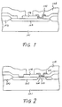
- a known semiconductor device is shown in Fig. 2, where a diffused layer formed in a silicon substrate is used as one electrode of a storage element.
- the silicon substrate indicated by 201, is of the P type.
- Created on the substrate 201 are an oxidized film 202 forming a field-insulating film, an N+ -type diffused layer 203, an interlayer insulting film 204, an N ⁇ -type diffused layer 205, a platinum silicide layer 206, an amorphous silicon film 207, and a film 208 for forming metal interconnections.
- the insulating film 204 is made from silicon oxide, for example.
- the N ⁇ -type diffused layer 205 is in contact with the N+-type diffused layer 203.
- the platinum silicide layer 206, the amorphous silicon film 207, and the film 208 for forming metal interconnections are laminated on the diffused layer 205 which serves as lower electrodes.
- the film 208 acts as upper electrodes. In the operation, an electric field is applied between the upper and lower electrodes to cause an avalanche breakdown in the amorphous silicon film. At this time, Joule heat is evolved to change parts of the amorphous silicon film, thus forming low-resistance regions.
- the rectifying function of the Schottky diode between the platinum silicide layer and the N ⁇ -type diffused layer is combined with the low-resistance regions of the amorphous silicon film to provide the known, electrically programmalbe read-only memory.
- This device has a polycrystalline silicon layer which is formed on a silicon substrate and acts as one electrode of each storage element.
- a polycrystalline silicon layer is heavily doped so as to exhibit N type.
- Another polycrystalline silicon layer formed on the heavily doped silicon layer is lightly doped and of the N type.
- a platinum silicide layer, an amorphous silicon film, and a film forming metal interconnections are deposited on the lightly doped polycrystalline silicon layer. The film forming the metal interconnections forms upper electrodes. Schottky diodes that are created between the platinum silicide layer and the lightly doped N-type polycrystalline silicon layer are employed.
- the lightly doped N-type diffused layer is formed to create the Schottky junctions. This presents the following problems.
- IPEL ion-implanted programmable element
- the first semiconductor layer is of the N type, for example.
- the second semiconductor layer formed on the N-type semiconductor layer is an amorphous semiconductor film, a polycrystalline semiconductor film, or a semiconductor film whose crystalline structure has been destroyed by ion implantation or an other technique, and each film is lightly doped with a P-type impurity.
- a P-type impurity exists between lattices in the noncrystalline or polycrystalline semiconductor film.
- the film is electrically inactive and, therefore, it shows a high resistance irrespective of the direction of the applied electric field. Once a high electric field is applied to the film deposited on the N-type semiconductor layer as lower electrodes, an avalanche breakdown take place, producing excessive electric current.
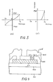
- a semiconductor device embodying the concept of the invention comprises a P-type semiconductor substrate 101 consisting of silicon or another material, an oxidized film 102 locally formed on the substrate and constituting a field-insulating film and consisting of silicon oxide, for example, an N+-type diffused layer 103, an interlayer insulating film 104 consisting of silicon oxide, for example, an amorphous silicon film 105 containing a P-type impurity, and a film 106 forming metal interconnections.
- the film 106 consists of one or more layers formed from Al, or a metal having a high melting point such as Mo, Ti, or W, or a silicide of such a high-melting point metal.
- the amorphous silicon film 105 having the P-type impurity and the upper electrode consisting of the film 106 are formed over the N+-type diffused layer 103 that forms the lower electrodes.
- This semiconductor device is fabricated in the manner described below.
- the oxidized film 102 is locally formed on the P-type semiconductor substrate 101.
- ions of phosphorus of 4 x 1015 cm ⁇ 2 are injected into the silicon substrate 101 at 60 keV by an ion implantation technique to form the N+-type diffused layer 103 which becomes the lower electrodes of the programmable elements.
- a film of silicon oxide is deposited by a CVD process to form the interlayer insulating film 104. Openings necessary for direct connection with the N+-type diffused layer 103 are made. Also, openings required to make connection via the amorphous silicon film 105 containing the P-type impurity and constituting the main portions of the programmable elements are formed.
- SiH4 is decomposed by a CVD process at a low temperature of 560°C to deposit an amorphous silicon film up to a thickness of 0.15 ⁇ m.
- Boron fluoride of 1 x 10¹¹ to 1 x 1015 cm ⁇ 2 is introduced into the amorphous silicon film at 60 keV by ion implantation to obtain desired diode characteristics.
- the amorphous silicon film 105 containing the P-type impurity is formed.
- This amorphous film 105 is photolithographically patterned.
- a barrier metal and aluminum are sputtered to form a laminate, which is then photolithographically patterned to create the film 106 for forming conductive interconnections.
- the resistance of the thus formed device is irreversibly changed from a high value to a low value by the application of an electric field.
- the device shows rectification.
- the oxidized film 102 is formed by localized oxidation of silicon (LOCOS). It is also possible to form grooves in a semiconductor substrate and to insert an isulator in the grooves.
- the aforementioned barrier metal can be a metal having a high melting point such as Mo, Ti, or W, or a silicide or nitride of such a metal. Usually, the barrier metal is located under aluminum.
- ions of boron fluoride of 1 x 1015 cm ⁇ 2 are injected at 60 keV into the amorphous silicon film containing the P-type impurity. Openings required to make connection via the amorphous silicon film have a diameter of 1.2 ⁇ m.
- Fig. 3(a) shows the electrical characteristic of the device before it is programmed.
- Fig. 3(b) shows the electrical characteristic after the device has been programmed by applying an electric field to induce an avalanche breakdown and producing an electric current of 2 to 3 mA. Before the device is programmed, the electrical characteristic curve is substantially symmetrical with respect to the direction in which the voltage is applied.
- a positive voltage is applied to the upper electrode that is an aluminum film overlying the amorphous silicon film, a forward characteristic is exhibited. If a negative voltage is applied, a reverse characteristic is obtained.
- the characteristic curve is substantially symmetrical with respect to the direction in which the voltage is applied, and the resistance is low.
- FIG. 4 there is shown another semiconductor device according to the invention.
- This device is similar to the device shown in Fig. 1 except that the N+-type diffused layer 103 acting as the lower electrode and shown in Fig. 1 is replaced by an N+-type polycrystalline silicon film 403 on an oxide film 402.
- the device shown in Fig. 4 comprises a P-type semiconductor substrate 401, the locally formed oxidized film 402, the N+-type polycrystalline silicon film 403, an interlayer insulating film 404, an amorphous silicon film 405 containing a P-type impurity, and a film 406 forming metal interconnections.
- the film 406 consists of two layers, i.e., a barrier metal layer and an aluminum layer formed on it, in the same way as in the device already described in connection with Fig. 1.
- the use of the N+-type polycrystalline silicon film on the oxide film increases the degree of freedom to which the pattern is laid out. Further, the N+-type polycrystalline silicon acting as the lower electrode is surrounded by the insulating film consisting of the silicon oxide film. Therefore, the Joule heat generated on programming does not readily escape. Consequently, the device can be programmed with lower electric current.
- a further semiconductor device comprises a P-type semiconductor substrate 501, an insulating film 502 consisting of a locally formed oxidized film, a low-resistance film 503, an interlayer insulating film 504, an N+-type polycrystalline silicon film 505, an amorphous silicon film 506 containing a P-type impurity, and a film 507 forming metal interconnections.
- the low-resistance film 503 which acts as a lower electrode is made from a metal of a low resistance, such as Mo, Ti, or W, or a silicide of such a metal, such as MoSi2. Holes are formed in the interlayer insulating film 504.
- the substrate 501 is made from silicon. Silicon oxide is deposited on the substrate 501 to form the insulating film 502. Then, MoSi2 is sputtered on the insulating film 502 up to a thickness of 0.2 ⁇ m and photolithographically patterned to form the metal film 503 that serves as the lower electrodes of programmable elements. A silicon oxide film is deposited by a CVD process to form the interlayer insulating film 504. Holes extending through the insulating film 504 are formed at locations at which the N-type polycrystalline silicon film 505 and the amorphous silicon film 506 containing the P-type impurity are to be formed.
- the holes are formed in the insulating film 504 at locations at which direct connections with the metal film 503 forming the lower electrodes are made.
- N-type polycrystalline silicon is deposited up to a thickness of 0.2 ⁇ m.
- the polycrystalline silicon film 505 is etched into a desired pattern. Ions of phosphorus of 4 x 1015 cm ⁇ 2 are injected into the polycrystalline silicon at 60 keV by ion implantation, and then the laminate is annealed in an electric furnace to activate the impurities, thus forming the N-type polycrystalline silicon film 505.
- SiH4 is decomposed at a low temperature of 560°C by a CVD process to deposit amorphous silicon as a layer up to a thickness of 0.15 ⁇ m.
- Ions of boron fluoride of 1 x 10¹¹ to 1 x 1015 cm ⁇ 2 are implanted at 80 keV to obtain desired diode characteristics.
- the amorphous silicon film 506 containing a P-type impurity is formed.
- the doped amorphous silicon film 506 is etched into a desired pattern covering the N-type polycrystalline silicon film 505.
- a barrier metal and aluminum are successively sputtered to form the film 507 for forming the metal interconnections.
- this film 507 is patterned by photolithographic techniques. As a result, a read-only memory is created which can be programmed by dielectric breakdown.
- This device comprises a P-type semiconductor substrate 601, an insulating film 602 that is a locally formed oxidized film, a low-resistance film 603 made from a low-resistance metal or metal silicide, such as MoSi2, an N+-type polycrystalline silicon film 604 formed on the low-resistance film 603, an interlayer insulating film 605, an amorphous silicon film 606 containing a P-type impurity, and a film 607 forming metal interconnections.
- the low-resistance film 603 acts as a lower electrode.
- This semiconductor device is manufactured in the manner described below.
- the insulating film 602 consisting of a film of silicon oxide is formed on the semiconductor substrate 601 made from silicon.
- MoSi2 is sputtered on the laminate up to a thickness of 0.2 ⁇ m to form the metal film 603 which creates the lower electrodes of programmable elements.
- polycrystalline silicon is deposited on the laminate to a thickness of 0.2 ⁇ m.
- ions of phosphorus of 4 x 1015 cm ⁇ 2 are implanted at 60 keV, followed by annealing of the laminate inside an electric furnace to form the N-type polycrystalline silicon film 604.
- the metal film 603 and the N-type polycrystalline silicon film 604 are etched into a desired pattern by a photoetching technique. Then, silicon oxide is deposited as a film by chemical vapor deposition to form the interlayer insulating film 605. Holes extending through the insulating film are formed at locations at which the amorphous silicon film 606 containing a P-type impurity are to be formed, namely at locations at which direct connection with the N-type polysilicon film 604 forming a part of the lower electrode is to be made. Then, SiH4 is decomposed at a low temperature of 560°C by a CVD process to form the amorphous silicon layer of 0.15 ⁇ m thick.
- Ions of boron fluoride of 1 x 10¹¹ to 1 x 1015 cm ⁇ 2 are implanted at 80 keV to derive desired diode characteristics.
- the amorphous silicon film 606 containing a P-type impurity is formed and etched into a desired pattern.
- a barrier metal and aluminum are successively sputtered as films to form the film 607 creating metal interconnections.
- the laminate is etched into a desired pattern. In this way, a read-only memory which can be programmed by dielectric breakdown is made.
- the P-type semiconductor film can be P-type polycrystalline silicon. Also, it can be polycrystalline silicon or crystalline silicon whose crystalline structure has been destroyed by ion implantation or another technique.
- the P-type semiconductor film can be replaced with an N-type semiconductor film where the lower electrode is a P+-type diffused layer.
- the metal film forming the lower electrode is made from MoSi2. It is also possible to fabricate the metal film from TiSi2 or WSi2. Further, the metal film can be polycide.
- the semiconductor substrate can be either P-type silicon or N-type silicon.
- the lower electrodes are made from a metal such as Mo, Ti, or W, or silicide of such a metal. This lowers the resistance of the lower electrodes. Therefore, where programmed regions are arranged in series, they can be programmed with lower electric current.
- the semiconductor films having a P-type impurity between lattices are formed by chemical vapor deposition and ion implantation. These films can also be created by sputtering.
- the semiconductor films may be made from polycrystalline silicon into which ions of a P-type impurity are injected. Also, they may be polycrystalline silicon or crystalline silicon whose crystalline structure has been destroyed by ion implantation.
- the P-type semiconductor film has an impurity between lattices.
- the lower electrode is a P+ -type diffused layer
- the film may be a semiconductor film containing an N-type impurity between lattices. In the examples shown in Figs.
- the metal films forming the lower electrodes are made from MoSi2. These films may also made from TiSi2, WSi2, W, or Mo.
- the film 106, 406, 507, and 607 which create metal interconnections to form upper electrodes may be one or more layers of aluminum, or a high-melting point metal such as W, Ti, Mo, or silicide thereof. As described thus far, the present invention is not limited to the aforementioned four examples, but various changes and modifications may be made.
- the resistance of the first semiconductor film that is located just under a programmed film and has the first conductivity type is low. Also, it is not modulated with voltage. Since the structure is simple, the area of the patterned regions is small. In addition, the device is fabricated by simple processes. By forming the lower electrode over the substrate, the generated Joule heat is effectively utilized and so the device can be programmed with lower electric current. The resistance of the lower electrode is lowered by forming the lower electrode from a high-melting point metal such as Mo, Ti, or W, or silicide of such a metal, such as MoSi2, TiSi2, or WSi2. Hence, a read-only memory capable of operating at a high speed can be obtained.
- a high-melting point metal such as Mo, Ti, or W
- silicide of such a metal such as MoSi2, TiSi2, or WSi2.
Landscapes
- Semiconductor Memories (AREA)
Claims (8)
- Composant semi-conducteur comprenant:
une première couche semi-conductrice (103; 403; 505; 604) d'un premier type de conductivité;
une deuxième couche semi-conductrice (105; 405; 506; 606) qui est formée sur la première couche semi-conductrice et consiste en un semiconducteur amorphe, un semi-conducteur polycristallin ou un semi-conducteur à structure cristalline détruite, ladite deuxième couche semi-conductrice contenant des impuretés d'un deuxième type de conductivité différent du premier type de conductivité; et
une couche d'électrode supérieure (106; 406; 507; 607) superposée à ladite deuxième couche et reliée à celle-ci de façon conductrice;
caractérisé en ce que ladite deuxième couche semi-conductrice est susceptible, lors d'une exposition à un courant électrique résultant d'une tension appliquée entre ladite première couche semi-conductrice et ladite électrode supérieure, d'être soumise à une transition irréversible qui la fait passer d'un état de grande résistance à un état de petite résistance, et une diode est formée entre ladite première et ladite deuxième couches semi-conductrices dès lors que la deuxième couche semi-conductrice a pris ledit état de petite résistance. - Composant semi-conducteur selon la revendication 1, caractérisé en ce que ladite première couche semi-conductrice (103) est une couche diffusée, et ladite deuxième couche semi-conductrice (105) est en silicium polycristallin, en silicium amorphe ou en silicium à structure cristalline détruite.
- Composant semi-conducteur selon la revendication 1, caractérisé en ce que ladite première couche semi-conductrice (403) est une couche dopée en silicium polycristallin, et ladite deuxième couche semi-conductrice (405) est en silicium polycristallin, en silicium amorphe ou en silicium à structure cristalline détruite.
- Composant semi-conducteur selon la revendication 1, caractérisé en ce que ladite première couche semi-conductrice (505) est en silicium polycristallin dopé et est reliée par des ouvertures traversant une pellicule isolante intermédiaire (504) à une couche sous-jacente (503) en métal ou en composé métallique, et ladite deuxième couche semi-conductrice (506) est en silicium polycristallin, en silicium amorphe ou en silicium à structure cristalline détruite.
- Composant semi-conducteur selon la revendication 1, caractérisé en ce que ladite première couche semi-conductrice (604) est une couche de silicium polycristallin dopée formée sur une couche (603) d'un métal ou d'un composé métallique et ladite deuxième couche semi-conductrice (606) est reliée à la première couche semi-conductrice par des ouvertures traversant une pellicule isolante intermédiaire (605) et est en silicium polycristallin, en silicium amorphe ou en silicium à structure cristalline détruite.
- Composant semi-conducteur selon la revendication 1, 2, 3, 4 ou 5, caractérisé en ce que ladite couche d'électrode supérieure (106; 406; 507; 607) est formée d'un métal ou d'un composé métallique.
- Composant semi-conducteur selon la revendication 6, caractérisé en ce que ledit métal ou ledit composé métallique est constitué de Al, de Mo, de Ti, ou de W, ou d'un siliciure d'un tel métal.
- Composant semi-conducteur selon la revendication 4 ou 5, caractérisé en ce que ladite couche de métal ou de composé métallique consiste en une ou plusieurs couches formées de Mo, de Ti, ou de W, ou d'un siliciure d'un tel métal.
Applications Claiming Priority (8)
| Application Number | Priority Date | Filing Date | Title |
|---|---|---|---|
| JP258833/88 | 1988-10-14 | ||
| JP25883388 | 1988-10-14 | ||
| JP122525/89 | 1989-05-16 | ||
| JP12252689 | 1989-05-16 | ||
| JP122526/89 | 1989-05-16 | ||
| JP12252589 | 1989-05-16 | ||
| JP175167/89 | 1989-07-06 | ||
| JP1175167A JP2525672B2 (ja) | 1988-10-14 | 1989-07-06 | 半導体装置 |
Publications (2)
| Publication Number | Publication Date |
|---|---|
| EP0365932A1 EP0365932A1 (fr) | 1990-05-02 |
| EP0365932B1 true EP0365932B1 (fr) | 1994-08-31 |
Family
ID=27470862
Family Applications (1)
| Application Number | Title | Priority Date | Filing Date |
|---|---|---|---|
| EP89118999A Expired - Lifetime EP0365932B1 (fr) | 1988-10-14 | 1989-10-12 | Dispositif semi-conducteur |
Country Status (3)
| Country | Link |
|---|---|
| US (1) | US5093711A (fr) |
| EP (1) | EP0365932B1 (fr) |
| DE (1) | DE68917848T2 (fr) |
Families Citing this family (31)
| Publication number | Priority date | Publication date | Assignee | Title |
|---|---|---|---|---|
| US5989943A (en) * | 1989-09-07 | 1999-11-23 | Quicklogic Corporation | Method for fabrication of programmable interconnect structure |
| US5502315A (en) * | 1989-09-07 | 1996-03-26 | Quicklogic Corporation | Electrically programmable interconnect structure having a PECVD amorphous silicon element |
| US5614756A (en) * | 1990-04-12 | 1997-03-25 | Actel Corporation | Metal-to-metal antifuse with conductive |
| US5272101A (en) * | 1990-04-12 | 1993-12-21 | Actel Corporation | Electrically programmable antifuse and fabrication processes |
| US5404029A (en) * | 1990-04-12 | 1995-04-04 | Actel Corporation | Electrically programmable antifuse element |
| US5780323A (en) * | 1990-04-12 | 1998-07-14 | Actel Corporation | Fabrication method for metal-to-metal antifuses incorporating a tungsten via plug |
| US5541441A (en) * | 1994-10-06 | 1996-07-30 | Actel Corporation | Metal to metal antifuse |
| US5552627A (en) * | 1990-04-12 | 1996-09-03 | Actel Corporation | Electrically programmable antifuse incorporating dielectric and amorphous silicon interlayers |
| EP0480580A3 (en) * | 1990-09-10 | 1992-09-02 | Canon Kabushiki Kaisha | Electrode structure of semiconductor device and method for manufacturing the same |
| US5322812A (en) * | 1991-03-20 | 1994-06-21 | Crosspoint Solutions, Inc. | Improved method of fabricating antifuses in an integrated circuit device and resulting structure |
| US5701027A (en) * | 1991-04-26 | 1997-12-23 | Quicklogic Corporation | Programmable interconnect structures and programmable integrated circuits |
| US5110754A (en) * | 1991-10-04 | 1992-05-05 | Micron Technology, Inc. | Method of making a DRAM capacitor for use as an programmable antifuse for redundancy repair/options on a DRAM |
| JP2808965B2 (ja) * | 1992-02-19 | 1998-10-08 | 日本電気株式会社 | 半導体装置 |
| EP0558176A1 (fr) * | 1992-02-26 | 1993-09-01 | Actel Corporation | Anti-fusible du type métal-à-métal comprenant une couche de barrière améliorée contre la diffusion |
| US5284788A (en) * | 1992-09-25 | 1994-02-08 | Texas Instruments Incorporated | Method and device for controlling current in a circuit |
| US5308795A (en) * | 1992-11-04 | 1994-05-03 | Actel Corporation | Above via metal-to-metal antifuse |
| US5581111A (en) * | 1993-07-07 | 1996-12-03 | Actel Corporation | Dielectric-polysilicon-dielectric antifuse for field programmable logic applications |
| US5369054A (en) * | 1993-07-07 | 1994-11-29 | Actel Corporation | Circuits for ESD protection of metal-to-metal antifuses during processing |
| US5856234A (en) * | 1993-09-14 | 1999-01-05 | Actel Corporation | Method of fabricating an antifuse |
| US5592016A (en) * | 1995-04-14 | 1997-01-07 | Actel Corporation | Antifuse with improved antifuse material |
| US5789764A (en) * | 1995-04-14 | 1998-08-04 | Actel Corporation | Antifuse with improved antifuse material |
| JP3027195B2 (ja) * | 1995-06-02 | 2000-03-27 | アクテル・コーポレイション | 隆起タングステンプラグ アンチヒューズ及びその製造方法 |
| US5741720A (en) * | 1995-10-04 | 1998-04-21 | Actel Corporation | Method of programming an improved metal-to-metal via-type antifuse |
| US5909049A (en) | 1997-02-11 | 1999-06-01 | Actel Corporation | Antifuse programmed PROM cell |
| JP3488681B2 (ja) * | 1999-10-26 | 2004-01-19 | シャープ株式会社 | 液晶表示装置 |
| EP1169739A1 (fr) * | 1999-12-08 | 2002-01-09 | Koninklijke Philips Electronics N.V. | Dispositif semi-conducteur a diode et son procede de fabrication |
| US6344669B1 (en) * | 2000-06-13 | 2002-02-05 | United Microelectronics Corp. | CMOS sensor |
| US6633182B2 (en) | 2001-09-05 | 2003-10-14 | Carnegie Mellon University | Programmable gate array based on configurable metal interconnect vias |
| US20050035429A1 (en) * | 2003-08-15 | 2005-02-17 | Yeh Chih Chieh | Programmable eraseless memory |
| US7132350B2 (en) | 2003-07-21 | 2006-11-07 | Macronix International Co., Ltd. | Method for manufacturing a programmable eraseless memory |
| US7180123B2 (en) * | 2003-07-21 | 2007-02-20 | Macronix International Co., Ltd. | Method for programming programmable eraseless memory |
Family Cites Families (12)
| Publication number | Priority date | Publication date | Assignee | Title |
|---|---|---|---|---|
| GB1399163A (en) * | 1972-11-08 | 1975-06-25 | Ferranti Ltd | Methods of manufacturing semiconductor devices |
| US4174521A (en) * | 1978-04-06 | 1979-11-13 | Harris Corporation | PROM electrically written by solid phase epitaxy |
| CA1136773A (fr) * | 1978-08-14 | 1982-11-30 | Norikazu Ohuchi | Dispositif semiconducteur |
| US4442507A (en) * | 1981-02-23 | 1984-04-10 | Burroughs Corporation | Electrically programmable read-only memory stacked above a semiconductor substrate |
| US4424579A (en) * | 1981-02-23 | 1984-01-03 | Burroughs Corporation | Mask programmable read-only memory stacked above a semiconductor substrate |
| DE3279114D1 (en) * | 1981-05-15 | 1988-11-17 | Fairchild Semiconductor | Schottky diode - polycrystalline silicon resistor memory cell |
| US4431460A (en) * | 1982-03-08 | 1984-02-14 | International Business Machines Corporation | Method of producing shallow, narrow base bipolar transistor structures via dual implantations of selected polycrystalline layer |
| US4590589A (en) * | 1982-12-21 | 1986-05-20 | Zoran Corporation | Electrically programmable read only memory |
| US4583106A (en) * | 1983-08-04 | 1986-04-15 | International Business Machines Corporation | Fabrication methods for high performance lateral bipolar transistors |
| US4598386A (en) * | 1984-04-18 | 1986-07-01 | Roesner Bruce B | Reduced-area, read-only memory |
| JPS62104066A (ja) * | 1985-10-31 | 1987-05-14 | Toshiba Corp | 半導体保護装置 |
| US4823181A (en) * | 1986-05-09 | 1989-04-18 | Actel Corporation | Programmable low impedance anti-fuse element |
-
1989
- 1989-10-11 US US07/419,657 patent/US5093711A/en not_active Expired - Lifetime
- 1989-10-12 DE DE68917848T patent/DE68917848T2/de not_active Expired - Fee Related
- 1989-10-12 EP EP89118999A patent/EP0365932B1/fr not_active Expired - Lifetime
Also Published As
| Publication number | Publication date |
|---|---|
| EP0365932A1 (fr) | 1990-05-02 |
| DE68917848T2 (de) | 1995-02-02 |
| US5093711A (en) | 1992-03-03 |
| DE68917848D1 (de) | 1994-10-06 |
Similar Documents
| Publication | Publication Date | Title |
|---|---|---|
| EP0365932B1 (fr) | Dispositif semi-conducteur | |
| EP0118158B1 (fr) | Structure ROM programmable et procédé de fabrication d'une telle structure | |
| US4551908A (en) | Process of forming electrodes and interconnections on silicon semiconductor devices | |
| EP0250078B1 (fr) | Elément d'interconnexion programmable à basse impédance | |
| EP0095411B1 (fr) | Cellule de mémoire bipolaire | |
| US4943538A (en) | Programmable low impedance anti-fuse element | |
| US5210598A (en) | Semiconductor element having a resistance state transition region of two-layer structure | |
| US5144404A (en) | Polysilicon Schottky clamped transistor and vertical fuse devices | |
| JPS60226163A (ja) | シヨツトキ−バイポ−ラトランジスタを有するcmos構造を製造する方法 | |
| SE451514B (sv) | Programmerbar cell bestaende av en amorf cellkropp, samt net av sadana celler | |
| SE454307B (sv) | Programmerbar cell; samt net uppbyggt av sadana celler | |
| KR100196484B1 (ko) | 얇은 희생층을 사용하여 수직형 퓨즈 디바이스 및 쇼트키다이오드를 제조하는 방법 | |
| US4375717A (en) | Process for producing a field-effect transistor | |
| US4396930A (en) | Compact MOSFET device with reduced plurality of wire contacts | |
| US4835118A (en) | Non-destructive energy beam activated conductive links | |
| US5436496A (en) | Vertical fuse device | |
| EP0051500B1 (fr) | Dispositif semi-conducteur | |
| EP0080730B1 (fr) | Dispositif semi-conducteur comprenant des couches conductrices et procédé pour le fabriquer | |
| US4425379A (en) | Polycrystalline silicon Schottky diode array | |
| EP0172193B1 (fr) | Cellule de memoire morte programmable et son procede de fabrication | |
| EP0078220B1 (fr) | Interférences de silicium polycristallin pour transistors bipolaires en circuit flip-flop | |
| US4600933A (en) | Semiconductor integrated circuit structure with selectively modified insulation layer | |
| US5212102A (en) | Method of making polysilicon Schottky clamped transistor and vertical fuse devices | |
| KR940008564B1 (ko) | 반도체 소자 및 그 제조방법 | |
| EP0209654B1 (fr) | Dispositif semi-conducteur comprenant des électrodes d'interconnexion |
Legal Events
| Date | Code | Title | Description |
|---|---|---|---|
| PUAI | Public reference made under article 153(3) epc to a published international application that has entered the european phase |
Free format text: ORIGINAL CODE: 0009012 |
|
| AK | Designated contracting states |
Kind code of ref document: A1 Designated state(s): DE FR NL |
|
| 17P | Request for examination filed |
Effective date: 19901010 |
|
| 17Q | First examination report despatched |
Effective date: 19930208 |
|
| GRAA | (expected) grant |
Free format text: ORIGINAL CODE: 0009210 |
|
| AK | Designated contracting states |
Kind code of ref document: B1 Designated state(s): DE FR NL |
|
| REF | Corresponds to: |
Ref document number: 68917848 Country of ref document: DE Date of ref document: 19941006 |
|
| ET | Fr: translation filed | ||
| PLBE | No opposition filed within time limit |
Free format text: ORIGINAL CODE: 0009261 |
|
| STAA | Information on the status of an ep patent application or granted ep patent |
Free format text: STATUS: NO OPPOSITION FILED WITHIN TIME LIMIT |
|
| 26N | No opposition filed | ||
| PGFP | Annual fee paid to national office [announced via postgrant information from national office to epo] |
Ref country code: DE Payment date: 20061005 Year of fee payment: 18 |
|
| PGFP | Annual fee paid to national office [announced via postgrant information from national office to epo] |
Ref country code: NL Payment date: 20061015 Year of fee payment: 18 |
|
| NLV4 | Nl: lapsed or anulled due to non-payment of the annual fee |
Effective date: 20080501 |
|
| PG25 | Lapsed in a contracting state [announced via postgrant information from national office to epo] |
Ref country code: DE Free format text: LAPSE BECAUSE OF NON-PAYMENT OF DUE FEES Effective date: 20080501 |
|
| REG | Reference to a national code |
Ref country code: FR Ref legal event code: ST Effective date: 20080630 |
|
| PG25 | Lapsed in a contracting state [announced via postgrant information from national office to epo] |
Ref country code: NL Free format text: LAPSE BECAUSE OF NON-PAYMENT OF DUE FEES Effective date: 20080501 |
|
| PGFP | Annual fee paid to national office [announced via postgrant information from national office to epo] |
Ref country code: FR Payment date: 20061010 Year of fee payment: 18 |
|
| PG25 | Lapsed in a contracting state [announced via postgrant information from national office to epo] |
Ref country code: FR Free format text: LAPSE BECAUSE OF NON-PAYMENT OF DUE FEES Effective date: 20071031 |