EP0365950B1 - Circuit pour ajuster le point de déclenchement d'un clavier inductif - Google Patents
Circuit pour ajuster le point de déclenchement d'un clavier inductif Download PDFInfo
- Publication number
- EP0365950B1 EP0365950B1 EP89119109A EP89119109A EP0365950B1 EP 0365950 B1 EP0365950 B1 EP 0365950B1 EP 89119109 A EP89119109 A EP 89119109A EP 89119109 A EP89119109 A EP 89119109A EP 0365950 B1 EP0365950 B1 EP 0365950B1
- Authority
- EP
- European Patent Office
- Prior art keywords
- key
- circuit arrangement
- microcomputer
- arrangement according
- current pulse
- Prior art date
- Legal status (The legal status is an assumption and is not a legal conclusion. Google has not performed a legal analysis and makes no representation as to the accuracy of the status listed.)
- Expired - Lifetime
Links
- 230000001939 inductive effect Effects 0.000 title claims description 10
- 230000008878 coupling Effects 0.000 claims description 28
- 238000010168 coupling process Methods 0.000 claims description 28
- 238000005859 coupling reaction Methods 0.000 claims description 28
- 239000003990 capacitor Substances 0.000 claims description 22
- 230000001965 increasing effect Effects 0.000 claims description 15
- 230000035945 sensitivity Effects 0.000 claims description 10
- 230000000630 rising effect Effects 0.000 claims description 9
- 229910000859 α-Fe Inorganic materials 0.000 claims description 7
- 230000006870 function Effects 0.000 claims description 4
- 239000011159 matrix material Substances 0.000 claims description 2
- 230000004913 activation Effects 0.000 claims 1
- 230000000903 blocking effect Effects 0.000 description 40
- 238000010586 diagram Methods 0.000 description 9
- 230000007257 malfunction Effects 0.000 description 6
- 230000001960 triggered effect Effects 0.000 description 5
- 238000004804 winding Methods 0.000 description 5
- 230000000694 effects Effects 0.000 description 3
- 238000000034 method Methods 0.000 description 3
- 238000012360 testing method Methods 0.000 description 3
- 230000007423 decrease Effects 0.000 description 2
- 238000004519 manufacturing process Methods 0.000 description 2
- 238000013461 design Methods 0.000 description 1
- 238000011161 development Methods 0.000 description 1
- 238000005516 engineering process Methods 0.000 description 1
- 230000003993 interaction Effects 0.000 description 1
- 238000012544 monitoring process Methods 0.000 description 1
- 238000003825 pressing Methods 0.000 description 1
- 238000012549 training Methods 0.000 description 1
Images


Classifications
-
- H—ELECTRICITY
- H03—ELECTRONIC CIRCUITRY
- H03K—PULSE TECHNIQUE
- H03K17/00—Electronic switching or gating, i.e. not by contact-making and –breaking
- H03K17/14—Modifications for compensating variations of physical values, e.g. of temperature
-
- H—ELECTRICITY
- H03—ELECTRONIC CIRCUITRY
- H03K—PULSE TECHNIQUE
- H03K17/00—Electronic switching or gating, i.e. not by contact-making and –breaking
- H03K17/94—Electronic switching or gating, i.e. not by contact-making and –breaking characterised by the way in which the control signals are generated
- H03K17/965—Switches controlled by moving an element forming part of the switch
- H03K17/97—Switches controlled by moving an element forming part of the switch using a magnetic movable element
- H03K17/972—Switches controlled by moving an element forming part of the switch using a magnetic movable element having a plurality of control members, e.g. keyboard
-
- H—ELECTRICITY
- H03—ELECTRONIC CIRCUITRY
- H03K—PULSE TECHNIQUE
- H03K17/00—Electronic switching or gating, i.e. not by contact-making and –breaking
- H03K17/94—Electronic switching or gating, i.e. not by contact-making and –breaking characterised by the way in which the control signals are generated
- H03K17/965—Switches controlled by moving an element forming part of the switch
- H03K17/97—Switches controlled by moving an element forming part of the switch using a magnetic movable element
- H03K2017/9706—Inductive element
Definitions
- the invention relates to a circuit arrangement for setting the trigger point of contactlessly effective keys in a matrix-shaped, inductive keyboard, each key consisting essentially of a button with a ferrite pin fastened therein, which when actuated one above the other on a circuit board of the matrix-like keyboard immersed arranged windings and generates a coupling signal, and has the means for eliminating the effects of mechanical and electrical tolerances on the setting of the trigger point.
- Keyboards of the aforementioned type have been used for some time as part of the equipment of a computer workstation of known series.
- the trigger point on this known keyboard is adjusted via a two-stage adjustment.
- An IC module (SN 7445) is used as the power switch, for which a supply voltage of 5 V ⁇ 5% is required. Due to future difficulties in procurement for the IC SN 7445 and for the purpose of widening the tolerance in the supply voltage, the IC module should be replaced by seven PNP transistors. However, this has the consequence that the tolerance of the collector-emitter voltage of the current switches increases and thus the tolerance of the tripping point is increased. The tolerances are also increased by reducing the number of coil turns, which enables cost-optimized circuit board production. These intended measures would require an at least 3-stage adjustment for each individual row of keys for a keyboard in the previous technology for setting the trigger point.
- Tolerances that affect the trigger points in an inductive keyboard are caused by a variety of influences, for example by the manufacturing tolerances of the inserted ferrite pins in the key buttons, by the external coupling tolerances of the secondary coils, by the tolerance of the offset voltage of the sense amplifier, by the different internal resistances of the individual Signal switches in the multiplexer, due to temperature fluctuations and supply voltage tolerances, and due to different current edges of the pulse generator due to the different current switch thresholds.
- the object of the invention is to provide a circuit arrangement for setting the trigger point of an inductive keyboard and a functional monitoring thereof, by means of which the known difficulties in setting the trigger point in keyboards of the type described in the introduction can be overcome and a multi-stage adjustment can be omitted.
- each of the specified seven current switches is first blocked in order to charge a capacitor.
- a current switch By switching on a current switch a row of buttons is selected and at the same time a current pulse flows through the primary row coils until the capacitor is discharged.
- the slope of the rising edge is controlled by a microcomputer by changing the blocking period. This enables the trigger point of a key (or all keys) to be set to a specific key path.
- the previously required two-stage adjustment can be omitted, and moreover, the circuit board does not need to be plated through, since it is now possible to design the primary and secondary coils in a smaller number of turns.
- the value of the blocking period is derived, for example, from a reference signal.
- the basic coupling signal of the keys can serve as a reference signal.
- the value of the blocking period can also be defined as a fixed value of a table.
- the microcomputer can continuously monitor the functionality of each key without additional circuitry (for example by checking the pulse generator, the power switch and the sense amplifier) and trigger an error message if the lockout time value is derived from the basic coupling signals.
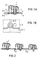
- each key element consists of a key button required for its actuation or, to put it more simply, a key 1 into which a ferrite pin 2 is inserted.
- the key 1 is guided in a key base housing 3 and forms a structural unit with the latter.
- the key base 3 can be placed on a circuit board 5 in correspondingly designed bores and is secured by latches on the key base 3 in the position of use in the circuit board 5.
- a spring 4 is supported on the one hand on the key base 3 and on the other hand on the key 1 and ensures that the key 1 returns to the starting position after each actuation.
- the ferrite pin 2 attached to it dips into primary (6/1) and secondary coils (6/2) arranged coaxially one above the other on the circuit board 5 of the keyboard and causes an inductive coupling of the primary coil 6/1 to the Secondary coil 6/2.
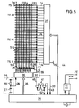
- the keyboard according to the exemplary embodiment according to FIG. 5 consists of a matrix-like arrangement of a total of 168 keys which are placed on the circuit board 5 at the intersection of seven rows of keys TR1 to TR7 with 24 key columns TS1 to TS24 running perpendicularly thereto.
- the primary coils 6/1 are in line loops 7 to 13 and are arranged on the top of the circuit board 5 (FIGURES 1A and 1B)), while the secondary coils 6/2 are provided accordingly on the underside of the circuit board 5 and in similar line loops 14 corresponding to that Key columns TS 1 to TS 24 are included.
- FIGURE 5 A schematic representation of an arrangement of the primary (6/1) and secondary coils (6/2) in a matrix is shown in FIGURE 5, in which the crossing points of the line loops 7 to 13 with the line loops 14 corresponding to the key columns TS 1 to TS 24, respectively symbolize the arrangement of a primary coil 6/1 to a secondary coil 6/2.
- the line loops 7 to 13 for the primary coils 6/2 are led back from the corresponding current switch 26 to the base 15 via the area of the key columns TS 1 to TS 24.
- the line loops 14 with the secondary coils 6/2 in the key columns TS 1 to TS 24 are connected, starting from a multiplexer 27, and the line loops TR 1 to TR 7 for the primary coils 6/1 are connected to a sense amplifier 32 (see FIG. 5).
- a basic coupling signal 39 is coupled from the primary coil 6/1 into the secondary coil 6/2 with each selected but not pressed key by a current pulse 28 (FIGURE 4F).
- This basic coupling signal 39 increases when the key is selected and pressed at the same time by the actual reading signal 39/1, which results from the more effective coupling of the primary (6/1) and secondary coils 6/2.
- An unselected key or a key with a malfunction does not provide a basic coupling signal 39.
- a key with a smaller basic coupling signal 39 results in a larger key travel s (FIGURE 2) to the trigger point if the steepness of the current pulse 28 is not changed. As a result of this, the tolerance of the trigger point can be recognized even when a button is not pressed (rest position).
- FIG. 5 In cooperation (FIGURE 5) between a microcomputer 24, a pulse generator 25, a power switch 26, a multiplexer 27 and a sense amplifier 32, the individual addresses of the keys are selected one after the other and thereupon queried whether a pressed key is present or not. This means that only when a key 1 is pressed, a current pulse 28 of the pulse generator 25 is transmitted from the primary coil 6/1 to the secondary coil 6/2 and is amplified by the sense amplifier 32 via a line 40 in the flip-flop 41 and over the microcomputer 24 and lines 42, 43 are stored in the key memory in the memory position assigned to this address as a key status bit.
- the tolerance of the trigger point of each key can be corrected, for example, by changing the ferrite pin position in key 1, or by changing the number of turns of the primary (6/1) and secondary coils 6/2, or by changing the steepness of the current pulse 28.
- the tolerance of the trigger point of each key can be corrected, for example, by changing the ferrite pin position in key 1, or by changing the number of turns of the primary (6/1) and secondary coils 6/2, or by changing the steepness of the current pulse 28.
- the tolerance of the trigger point of each key can be corrected, for example, by changing the ferrite pin position in key 1, or by changing the number of turns of the primary (6/1) and secondary coils 6/2, or by changing the steepness of the current pulse 28.
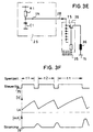
- a change in the slope of the driver current pulse edge by means of a pulse generator 25/2 according to the circuit according to FIG. 3A takes place in four stages and is controlled by the microcomputer 24 via a control line 37 and two further control lines 38/1 and 38/2.
- the three control lines 37, 38/1, 38/2 are each led via an OR gate 16, 17, 18 and a resistor R4, R5 and R6 to the base of PNP transistors T1, T2, T3, the emitters of which are connected via resistors R7, R8, R3 are connected to the current switches 26 via the common current pulse line 28.
- FIG. 3B shows a schematic pulse diagram which symbolizes the gradual increase in the steepness of the rising edge of the current pulses 28 due to the connection of the transistors T2 and T3 via the control lines 38/1 and 38/2.
- FIG. 3C A further exemplary embodiment for changing the steepness of the rising edge of the current pulse 28 is indicated in FIG. 3C.
- a pulse generator 25/1 specified in the circuit shown there in deviation from the aforementioned example (according to FIG. 3A), causes a continuous change in the slope of the rising edge of the current pulse 28.
- the pulse generator 25/1 according to FIG. 3C only has one Control line 37, which is connected to the base of the single transistor T1 via a resistor R2.
- the emitter voltage U E is determined by a capacitor C1 connected in series with a resistor R1.
- the collector line is connected to the current switches 26 in order to transmit the current pulse 28.
- the capacitor C1 is charged via the resistor R1 according to an e-function until the control line 37 assumes a low level (FIGURE 3D) and then the capacitor C1 goes over Transistor T1 and a transistor T5 of the current switch 26 and the primary series coils 36 (or 6/1) can discharge.
- the steepness of the current pulse 28 is determined by the level of the voltage at the emitter of T1 and is controlled by the microcomputer 24 by changing the blocking time t1 to tn via the control line 37.
- a pulse generator 25 In a further preferred embodiment of a pulse generator 25 according to FIGURE 3E and FIGUR 6, the previously required control line 37 as well as the transistor T1 and the resistor R2 are dispensed with compared to the previously explained pulse generator 25/1, which alone brings about a significant simplification and savings in terms of component expenditure .
- the pulse generator 25 only consists of the capacitor C1 connected in series with the resistor R1, between which an emitter voltage U E is tapped and applied to the seven current switches 26.
- this pulse generator 25 is as follows: First, the seven current switches 26, specifically the transistors T5, are blocked by a high level on the seven control lines 35 in order to charge a capacitor C1 via the resistor R1. By turning on a power switch 26 at a low level on a control or. Port line 35, the blocking time t1 to tn is ended, and at the same time a current pulse 28 flows through the correspondingly controlled transistor T5 of the current switch 26 via the primary coils 6/1 of the key primary row coils 36 until the capacitor C1 is discharged (FIG. 3E).
- the steepness of the current pulse 28 (see FIGURE 3F) is controlled by the microcomputer 24 in that it can change the blocking time t1 to tn for each individual key.
- the blocking time t1 is changed, e.g. B. extended into a blocking time t2
- the rising edge of the current pulse 28 becomes steeper because the capacitor C1 is charged to a higher voltage value U E.
- the pulse height of the basic coupling (39) and read signal 39/1 increases, and the key travel s to the trigger point of the corresponding key decreases.
- a blocking time value t1 to tn is provided for each individual key, which is in a value table or is stored as a changeable value in a read / write memory.
- FIG. 4A shows a sense amplifier 32, via which the basic coupling signal 39 or the read signal 39/1 is conducted on the output side of the secondary coils 6/2 (column coils) (FIG. 5).
- a signal on the output line 40 of a voltage amplifier 34 of the sense amplifier 32 is stored in a flip-flop 41 and can be queried by the microcomputer 24 via a line 42 by control via a line 43.
- the sensitivity of the sense amplifier 32 can be controlled via a control line 33.
- the supplied key signal 39, 39/1 is decoupled by a capacitor C10 in the sense amplifier 32 and supplied to the minus input of the amplifier 34.
- a negative bias voltage is applied to resistors R10, R11 and R12 at the input of amplifier 34.
- the plus input of amplifier 34 is connected to the base via a capacitor C11.
- the sensitivity is controlled via the control line 33, which is led via a resistor R16 to the base of a transistor T10.
- resistor R13 In series with resistor R11 and in parallel with resistor R12 there is a resistor R13 in the collector-emitter circuit.
- the transistor T10 is switched on by a high level and thereby the current through resistor R11 increases by the value of the current flowing through R13. This increases the voltage drop across resistor R11, and thus the negative bias voltage at the plus / minus input of amplifier 34 increases and the sensitivity of sense amplifier 32 decreases.
- the read signal 39/1 increases with increasing key travel s (between s1 and s2, FIGURE 2) and is decoupled in direct current via the capacitor C10 (FIGURE 4A) and fed to the sense amplifier 32.
- the positive read signal 39/1 has overcome the negative bias at the ⁇ input of the sense amplifier 32, its output on the output line 40 switches to a low level.
- the flip-flop 41 stores the key state (pressed / not pressed) until the corresponding key signal on line 42 can be queried by the microcomputer 24 (FIGURE 5).
- the basic coupling signal 39 has approximately half the signal level of a read signal 39/1.
- the sensitivity of the sense amplifier 32 must therefore be increased from 2 mm to 0 mm key travel (setting by means of basic coupling signals).
- the voltage divider R14, R15 compensates the tripping point if the supply voltage changes during the key query.
- the sensitivity of the sense amplifier 32 is reduced when the supply voltage increases, in the same ratio as the current pulse 28 increases in the steepness of the rising edges above the transistor threshold of the transistor T5 (FIG. 3E).
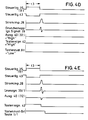
- the procedure is as follows: Each key is assigned an unchangeable value from t1 to tn. Accordingly, the blocking period can be changed in n steps. The respective values are measured once for each new keyboard circuit board (5) layout. For each key 1, the slope of the current pulse 28 is increased by increasing the blocking time of the correspondingly assigned current switches 26 (or transistors T5) until the key 1 is triggered in half the key path. The locking time t determined is stored in a table as a "program mask". There is no lock time determination as shown in FIGURE 7A. It is therefore also not necessary that every key (except for the key 7/1 shown in the example in FIG. 5) is in the rest position after the supply voltage has been switched on.
- the microcomputer 24 selects the key 7/1 (same as key in key row 7 and key column 1) after switching on the supply voltage (see FIGURE 4B, 4C, FIGURE 6, block 51) .
- the functional flow in this regard is explained below with reference to the explanations for FIG. 6.
- the logic flow diagram according to FIG. 6 serves to explain individual method steps in the circuit arrangement according to FIG. 5, the sequence of which is as follows:
- block 50 (FIG. 6) is called up.
- Block 51 is then called.
- Key 7/1 (in key row TR7 and key column TS1) is selected by first switching the secondary coils 6/2 in key column TS1 to ground via multiplexer 27 via control lines 44 (FIGURE 5) so that the read signal 39/1 for the key column TS1 can take effect.
- the current pulse 28 is triggered at the end of the blocking time t15 by switching on the current switch 26 for the row of keys TR7.
- the capacitor C1 can now discharge via the corresponding current switch 26 for the key row TR7 and via all primary row coils 6/1 in TR7 according to position 36 (FIGURE 3E) (see also FIGURES 4B, 4C).
- the program flow is continued in accordance with block 52 in FIG. 6 by querying the key signal on line 42.
- a key signal is recognized when the signal level of the basic coupling signal 39 of the relevant key is higher than the negative bias voltage at the +/- input of the sense amplifier 32. The consequence is that the sense amplifier 32 delivers a short "low” pulse at the output 40, which is buffered in the flip-flop 41 and brings the key signal on the line 42 to a "low” level until the microcomputer 24 can query the key signal line 42.
- block 53 is not called (FIG. 4B) because the control line 33 is not changed and block 54 is therefore called directly.
- the change on the control line 33 reduces the negative bias voltage at the +/- input of the sense amplifier 32, because by blocking the transistor T10 the current through the resistor R11 is reduced by the value which additionally flowed through the resistor R13.
- the read amplifier 32 is only set once because repeating the setting while the key was being pressed while the 7/1 key was pressed would result in the read amplifier 32 being set incorrectly.
- the key query begins with the selection of key 1/1.
- the secondary coils 6/2 for the key column TS1 are selected as in block 51.
- Each current switch 26 is then blocked with a blocking time value t3, which is stored in a value table in the microcomputer 24.
- This value t3 defined for the key 1/1 reduces the key trigger tolerance of the key 1/1 the better, the more of the n levels from t1 to tn can be selected by the microcomputer 24.
- the current pulse 28 is triggered by the end of the blocking time t3.
- FIGURE 4D shows the functional sequence of the key 1/1, in which no key change is determined because it is in the idle position, and block 57 is therefore selected directly.
- FIGURE 4E the pressed key 1/1 is selected and a change in the key of the key 1/1 is determined. In this case, block 56 is called.
- a key change is determined by an exclusive OR combination of the key status bit and the key signal on line 42.
- the statement “yes” only occurs if that Key state bit has a “low” state and a key signal on line 42 is recognized (FIGURE 4E), or when the key state bit is in a "high” state and no key signal on line 42 is recognized.
- Block 56 there is a message "Key 1/1 is pressed", i. H. this state of the key 1/1 is passed on to the central unit ZE with a code via an interface 31.
- the key status bit of the key 1/1 is set to the "high” state. If the key 1/1 is pressed during the next selection, the key status bit of the key 1/1 is set to "high” and a key signal is recognized at the same time, and thus no key change can be determined in block 55.
- block 57 is called up by selecting keys 2 to 168 and evaluating them accordingly. After the end of block 57, one key cycle has ended and block 54 is selected again.
- a further possibility of setting the trigger point results from an arrangement according to which the value of the blocking period is derived from the basic coupling signals of the keys.
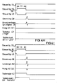
- the sequence of setting the trigger point with basic coupling signals is indicated in the flow chart according to FIGURES 7A and 7B.
- a prerequisite during the lock time determination is that each key is in the rest position.
- FIGURE 7A After switching on the keyboard supply voltage block 60 is called (FIGURE 7A).
- the key status bits in the read / write memory of the microcomputer 24 are first deleted and the sense amplifier 32 (see FIGURES 4A, 4F and 5) is set to sensitive with a "low” level on the control line 33.
- the change from "High” to “Low” causes a 2 mm earlier button release.
- block 61 is called up by selecting the key 1/1 with the blocking time t1 (FIGURE 4F).
- the current pulse 28 is triggered by the end of the blocking time t1.
- the capacitor C1 can now discharge via the primary coils 6/1 in the row of keys TR1.
- the program sequence is continued with the call of block 62 with the interrogation of the key signal 42. According to FIG. 4F, no key signal can be determined for key 1/1, and block 64 is thus called.
- Block 63 the value "1" is stored in a blocking time register SR 1 for the key 1/1. Block 70 is then called.
- block 65 the query regarding a key signal on line 42 of key 1/1 takes place again.
- the condition is also not fulfilled for the blocking time t2 (see FIGURE 4F), and therefore block 67 is called.
- block 68 follows with the renewed query of the key signal on line 42.
- the condition "key signal recognized" according to FIG. 4F is now fulfilled, because now the basic coupling signal 39 of the key 1/1, which has been increased again, changes output 40 of sense amplifier 32 to a Low "pulse can switch.
- block 71 is called after block 68.
- the value "3" is stored in the blocking time register SR1.
- the maximum blocking time t3 is necessary. Subsequent selection of the 1/1 key always takes place with the blocking time value t3 stored in the blocking time register SR1.
- block 70 is called.
- the values of the blocking times for keys 2 to 168 are now determined and stored accordingly in the blocking time register SR2 to SR168 (see FIGURES 4H, 4I). Then the sensitivity of the sense amplifier 32 is reduced by a "high" level via the control line 33, so that a key signal can only be recognized when the keys are pressed.
- FIG. 4D shows the functional sequence of the key selection of key 1/1 when key 1/1 is in the idle position, or FIGURE 4E when key 1/1 is pressed.
- the block 70 is called after block 70.
- the selection of the key 1/1 occurs with the blocking time value t3 from the blocking time register SR1 (see FIGURES 4H, 4I).
- block 72 After block 72, a query is made in block 73 with the condition "key change recognized by key 1/1". If the key 1/1 is now in the rest position, block 75 is called (FIGURE 4H). If, on the other hand, the condition "key change recognized" is met, the sequence according to FIG. 4I is shown and block 74 is called.
- Block 76 is followed by block 76.
- the 1/1 key is checked for functionality (see FIGURE 4G).
- a "low" level of the control line 33 increases the sensitivity of the sense amplifier 32, so that when the key 1/1 is not pressed, a key signal on line 43 can be recognized if the key 1/1 is functional.
- block 76 is followed by the query according to block 77 with the condition "key signal recognized?".
- FIGURE 4G shows the functional sequence if the key 1/1 has a malfunction and thus block 79 is called.
- block 78 is called.
- keys 2 to 168 are examined for a malfunction (see FIGURE 4G).
- an error message is sent to the central unit ZE as in block 79.
- the control line 33 must be set to a "high" level, i. H. the sense amplifier 32 must be switched to insensitive.
- the triggering point of the buttons can only be set in four steps using the basic coupling signal if only two bits are available for the value of the blocking period.
- a tripping tolerance of 3 mm must be compensated for.
- the setting of the trigger point by means of a basic coupling signal proves to be a practical solution.
- the best way to easily set the trigger point is to use a table of values. It is also conceivable to store several different value tables in order to record a shift in the trigger points caused by a general change in the keyboard, for example.
Landscapes
- Input From Keyboards Or The Like (AREA)
Claims (14)
- Dispositif de commande pour le réglage du point de déclenchement de touches agissant sans contact, sur un clavier inductif de type matriciel, chaque touche (1) étant composée essentiellement d'une tête de touche (1a) à laquelle est fixée une cheville en ferrite (2) qui, lorsque l'on actionne une touche, descend dans des bobines primaire et secondaire (6/1, 6/2) superposées et disposées sur une plaquette à circuits imprimés (5) du clavier, et produit un signal de couplage, caractérisé en ce qu'il comporte un générateur d'impulsions (25), et un commutateur de courant (26) commandé par un micro-ordinateur (24), et par l'intermédiaire duquel le générateur d'impulsions (25) peut être connecté à la bobine primaire (6/1) associée à une touche (1) sélectionnée, en ce que le micro-ordinateur (24) est connecté au générateur d'impulsions (25) et/ou au commutateur de courant (26) par l'intermédiaire de lignes de commande (37, 38/1, 38/2, 35), pour commander automatiquement la raideur de pente du signal de l'impulsion de commande amenée à la bobine primaire (6/1), en fonction d'une valeur présélectionnable déterminant le point de déclenchement de la touche (1), et en ce que la bobine secondaire (6/2) associée à la touche sélectionnée (1) est connectée à un flip-flop (41) par l'intermédiaire d'un amplificateur de lecture (32), pour fournir au micro-ordinateur (24) un signal représentatif de chacun des états de la touche.
- Dispositif de commande selon la revendication 1, caractérisé en ce que le générateur d'impulsions (25, 25/1, 25/2)) prévu pour la production d'une impulsion de courant (28) peut être connecté, pour une disposition à sept rangées de touches (TR1 à TR7), aux bobines primaires (6/1) des rangées de touches (TR1 à TR7) par l'intermédiaire de sept commutateurs de courant (26) correspondants, et par des lignes de commande (35) pouvant être activées au choix par le micro-ordinateur (24).
- Dispositif de commande selon la revendication 2, caractérisé en ce que les sept commutateurs de courant (26) sont constitués selon une disposition à sept transistors PNP.
- Dispositif de commande selon la revendication 1, caractérisé en ce qu'une modification de la raideur de pente du flanc intérieur de l'impulsion de courant (28) est commandée par le micro-ordinateur (24) par l'intermédiaire d'une modification variable réglable d'une durée du temps inactif (t1 à tn) pour le commutateur de courant (26).
- Dispositif de commande selon la revendication 4, caractérisé en ce que chacun des sept commutateurs de courant (26) est d'abord inactif pour une durée déterminée du temps inactif, pour charger un condensateur (C1), et en ce qu'une rangée de touches (TR1 à TR7) est sélectionnée par la mise en circuit d'un commutateur de courant (26) en même temps qu'une impulsion de courant (28) passe par les bobines primaires (6/1) de la rangée de touches sélectionnée (TR1 à TR7), jusqu'à ce que le condensateur (C1) soit chargé.
- Dispositif de commande selon la revendication 5, caractérisé en ce que la commande de la durée du temps inactif (t1 à tn) du commutateur de courant (26), ainsi que la mise en circuit d'un commutateur de courant (26) pour l'activation d'une rangée de touches (TR) sont assurées par l'intermédiaire de lignes de commande (35) du micro-ordinateur (24).
- Dispositif de commande selon la revendication 2, caractérisé en ce qu'un émetteur d'impulsions (25/2) est prévu pour une modification graduelle de la raideur de pente de l'impulsion de courant (28), celui-ci (25/2) présentant une ligne de commande (37) comportant un transistor (T1), et deux autres lignes de commande (38/1 et 38/2) pouvant être mises en circuit et comportant deux transistors de commutation (T2 et T3), de telle sorte que, à un niveau bas , les transistors (T1, T2, T3) passent en connexion par l'intermédiaire des lignes de commande (37, 38/1, 38/2), et la raideur de pente de l'impulsion de courant (28) peut ainsi être augmentée graduellement.
- Dispositif de commande selon la revendication 2, caractérisé en ce qu'un émetteur d'impulsion (25/1) est prévu pour une modification graduelle de la raideur de pente de l'impulsion de courant (28), lequel émetteur est composé d'un circuit RC pour la formation d'une tension émetteur (UE), d'un transistor (T1), le condensateur (C1) étant chargé selon une fonction-e tant qu'existe sur la ligne de commande (37) un niveau haut à la base d'un transistor (T1), et le condensateur (C1) pouvant se décharger par l'intermédiaire des bobines primaires (6/1), lorsque la ligne de commande (37) adopte un niveau bas , la raideur de pente de l'impulsion de courant (28) étant déterminée par la hauteur de la tension (UE) au niveau de l'émetteur, et pouvant être commandée par la modification réglable par le micro-ordinateur (24) du temps inactif (t1 à tn) sur la ligne de commande (37).
- Dispositif de commande selon la revendication 2, caractérisé en ce qu'un générateur d'impulsions (25) est prévu pour un réglage automatique du point de déclenchement, lequel générateur est composé d'une résistance (R1) et d'un condensateur (C1), connecté à sept commutateurs de courant (26), de telle sorte que les sept commutateurs de courant (26) sont inactifs sur les sept lignes de commande (35) au-dessus d'un niveau haut , pour charger le condensateur (C1) par l'intermédiaire de la résistance (R1), et de telle sorte qu'un commutateur de courant (26) devient conducteur à un niveau bas sur une ligne de commande (35), que le temps inactif (t1 à tn) se termine, et qu'une impulsion de courant (28) passe par l'intermédiaire d'un transistor (T5) jusqu'à ce que le condensateur (C1) soit déchargé.
- Dispositif de commande selon la revendication 9, caractérisé en ce que la raideur de pente d'une impulsion de courant (28) est commandée de façon variable par un micro-ordinateur (24), la valeur du temps inactif (t1 à tn) pouvant être modifiée par ce dernier (24) pour chacune des touches (1), et une valeur de temps inactif (t1 à tn) pouvant ainsi être associée à chacune des touches.
- Dispositif de commande selon la revendication 10, caractérisé en ce qu'un temps inactif (t1 à tn) déterminé une fois pour toutes et associé à chacune des touches (1) est consigné sous forme de valeur non modifiable sur un tableau de valeurs.
- Dispositif de commande selon la revendication 10, caractérisé en ce qu'une valeur du temps inactif est prévue pour chacune des touches (1), laquelle valeur est consignée sous forme de valeur pouvant être modifiée dans une mémoire à lecture-écriture du micro-ordinateur (24).
- Dispositif de commande selon la revendication 1, caractérisé en ce qu'est prévu un amplificateur de lecture (32) dont la sensibilité peut être commandée par le micro-ordinateur (24) par l'intermédiaire d'une ligne de commande (33), de façon à ce qu'un passage de l'état haut à l'état bas sur la ligne de commande (33) assure un déclenchement anticipé, pouvant varier de 2 mm, d'un signal de touche au niveau de la sortie (40), de telle sorte qu'une touche (1) capable de fonctionner fournit un signal de touche qui atteint la hauteur d'un signal de couplage de base (39) pour commuter l'amplificateur de lecture (32) sur une impulsion bas au niveau de la sortie (40).
- Dispositif de commande selon la revendication 1, caractérisé en ce qu'un flip-flop (41) est prévu du côté sortie de l'amplificateur de lecture (32), pour conserver un signal de touche existant jusqu'à ce qu'intervienne un appel d'un signal de touche par le micro-ordinateur (24) par l'intermédiaire des lignes de commande (42, 43).
Applications Claiming Priority (2)
| Application Number | Priority Date | Filing Date | Title |
|---|---|---|---|
| DE3836733 | 1988-10-28 | ||
| DE3836733A DE3836733A1 (de) | 1988-10-28 | 1988-10-28 | Schaltungsanordnung zur einstellung des ausloesepunktes in einer induktiven tastatur |
Publications (3)
| Publication Number | Publication Date |
|---|---|
| EP0365950A2 EP0365950A2 (fr) | 1990-05-02 |
| EP0365950A3 EP0365950A3 (fr) | 1991-04-10 |
| EP0365950B1 true EP0365950B1 (fr) | 1996-04-10 |
Family
ID=6366097
Family Applications (1)
| Application Number | Title | Priority Date | Filing Date |
|---|---|---|---|
| EP89119109A Expired - Lifetime EP0365950B1 (fr) | 1988-10-28 | 1989-10-14 | Circuit pour ajuster le point de déclenchement d'un clavier inductif |
Country Status (3)
| Country | Link |
|---|---|
| US (1) | US5066951A (fr) |
| EP (1) | EP0365950B1 (fr) |
| DE (2) | DE3836733A1 (fr) |
Families Citing this family (8)
| Publication number | Priority date | Publication date | Assignee | Title |
|---|---|---|---|---|
| US5510783A (en) * | 1992-07-13 | 1996-04-23 | Interlink Electronics, Inc. | Adaptive keypad |
| CA2192230A1 (fr) * | 1996-12-05 | 1998-06-05 | Rich Chen | Interrupteur electromagnetique |
| CN1059288C (zh) * | 1997-04-01 | 2000-12-06 | 旭丽股份有限公司 | 电磁感应开关 |
| US20040017302A1 (en) * | 2002-07-23 | 2004-01-29 | Kylink Communications Corp. | Matrix keyboard circuit for attenuating electromagnetic interference |
| KR101022477B1 (ko) * | 2004-11-25 | 2011-03-15 | 삼성전자주식회사 | 자기력을 이용하는 키 입력장치와 그의 동작방법 및컴퓨터 프로그램을 저장하는 컴퓨터로 읽을 수 있는기록매체 |
| DE102007052146A1 (de) * | 2007-10-31 | 2009-05-07 | Hypercom Gmbh | Tastatur mit einem magnetisch sensitiven Element |
| US20120242515A1 (en) * | 2011-03-24 | 2012-09-27 | Diehl Ako Stiftung & Co. Kg | Inductive touch sensing circuit providing sensitivity compensation |
| FR3038642B1 (fr) * | 2015-07-08 | 2017-07-14 | Continental Automotive France | Dispositif de detection d'intention de verrouillage ou de deverrouillage d'une portiere de vehicule automobile par un utilisateur |
Family Cites Families (11)
| Publication number | Priority date | Publication date | Assignee | Title |
|---|---|---|---|---|
| US3522442A (en) * | 1968-06-04 | 1970-08-04 | Ferranti Packard Ltd | Switch |
| GB1270892A (en) * | 1969-09-01 | 1972-04-19 | Olivetti & Co Spa | Keyboard for calculating machines, teleprinters, terminals and the like |
| US3638221A (en) * | 1969-11-24 | 1972-01-25 | Illinois Tool Works | Solid-state keyboard |
| US3668697A (en) * | 1970-09-24 | 1972-06-06 | Hewlett Packard Co | Noncontacting keyboard |
| US3765014A (en) * | 1970-10-12 | 1973-10-09 | Syner Data Inc | Keyboard |
| US3772684A (en) * | 1972-01-26 | 1973-11-13 | Scantlin Elect Inc | Push button keyboard with oscillator keying |
| US4117438A (en) * | 1977-04-13 | 1978-09-26 | Datanetics Corporation | Contactless keyswitch for keyboards |
| US4494109A (en) * | 1978-09-27 | 1985-01-15 | Bernin Victor M | Noncontacting keyboard employing a transformer element |
| US4300127A (en) * | 1978-09-27 | 1981-11-10 | Bernin Victor M | Solid state noncontacting keyboard employing a differential transformer element |
| US4398180A (en) * | 1980-06-26 | 1983-08-09 | International Standard Electric Corporation | Contactless keyboard |
| US4529967A (en) * | 1982-07-15 | 1985-07-16 | Gifft Thomas H | Non contacting inductive keyboard |
-
1988
- 1988-10-28 DE DE3836733A patent/DE3836733A1/de active Granted
-
1989
- 1989-10-14 EP EP89119109A patent/EP0365950B1/fr not_active Expired - Lifetime
- 1989-10-14 DE DE58909645T patent/DE58909645D1/de not_active Expired - Fee Related
- 1989-10-24 US US07/426,893 patent/US5066951A/en not_active Expired - Fee Related
Also Published As
| Publication number | Publication date |
|---|---|
| US5066951A (en) | 1991-11-19 |
| DE3836733A1 (de) | 1990-05-03 |
| EP0365950A2 (fr) | 1990-05-02 |
| EP0365950A3 (fr) | 1991-04-10 |
| DE3836733C2 (fr) | 1990-08-16 |
| DE58909645D1 (de) | 1996-05-15 |
Similar Documents
| Publication | Publication Date | Title |
|---|---|---|
| EP0228019B1 (fr) | Commutateur de proximité fonctionnant sans contact | |
| DE2707052C2 (fr) | ||
| EP1191693A1 (fr) | Circuit pour surveiller le courant dans un transistor de puissance | |
| EP0365950B1 (fr) | Circuit pour ajuster le point de déclenchement d'un clavier inductif | |
| EP0132850A1 (fr) | Commutateur de proximité auto-contrôlé | |
| DE3507130A1 (de) | Treiberstromkreis fuer eine magnetspule | |
| DE2835222A1 (de) | Polaritaetsempfindliche josephson- schaltung | |
| DE1424528B2 (de) | Leseschaltung mit erhoehter ablesegeschwindigkeit fuer einen oberflaechenspeicher mit einem eine magnetisierbare oberflaeche spurweise abtastenden bewickelten lesekopf | |
| DE3017827A1 (de) | Integrierte schaltung zur ueberwachung der anwesenheit eines externen systems | |
| DE3932083C1 (en) | Control circuitry for FET operating as switch in load circuit - provides voltage source dependent on control voltage of FET raising working point of controlled path by offset voltage | |
| DE1152143B (de) | Bistabiler Multivibrator | |
| DE2855342C2 (de) | Speicherschaltung | |
| DE8813549U1 (de) | Vorrichtung zur Einstellung des Auslösepunktes in einer induktiven Tastatur | |
| EP0607624B1 (fr) | Détecteur de déclenchement électrique pour appareil de vérification de pièces de monnaie alimenté par batterie | |
| DE3612182C2 (de) | RC-Oszillator | |
| DE1288138B (de) | Mit Stromuebernahme arbeitende Gatterschaltung | |
| DE4039422C2 (de) | Magnetfeldsensor | |
| DE19833210A1 (de) | Verstärkerschaltung zur Kapazitätsmessung | |
| DE1574759B2 (de) | Magnetkernspeicher mit gemeinsamer Schreib- und Leseleitung | |
| DE2539938A1 (de) | Schaltungsanordnung zur steuerung der einschaltung und zur ueberwachung eines laststromkreises | |
| DE1176714B (de) | Anordnung fuer eine statische magnetische Speichervorrichtung | |
| DE1524977C2 (de) | Schaltungsanordnung zur Aussteuerung eines Festwertspeichers mit induktiven Koppelelementen | |
| AT246464B (de) | Schaltkreissystem für taktgesteuerte elektronische Anlagen mit magnetischen Logikelementen | |
| AT235909B (de) | Schaltungsanordnung zum Sperren der Erregerspulen eines Mehrankerhaftrelais | |
| DE1962506C3 (de) | Halbfestwertspeicher mit zugehöriger Leseeinrichtung |
Legal Events
| Date | Code | Title | Description |
|---|---|---|---|
| PUAI | Public reference made under article 153(3) epc to a published international application that has entered the european phase |
Free format text: ORIGINAL CODE: 0009012 |
|
| AK | Designated contracting states |
Kind code of ref document: A2 Designated state(s): CH DE FR GB IT LI NL SE |
|
| PUAL | Search report despatched |
Free format text: ORIGINAL CODE: 0009013 |
|
| AK | Designated contracting states |
Kind code of ref document: A3 Designated state(s): CH DE FR GB IT LI NL SE |
|
| 17P | Request for examination filed |
Effective date: 19910813 |
|
| RAP1 | Party data changed (applicant data changed or rights of an application transferred) |
Owner name: DIGITAL-KIENZLE COMPUTERSYSTEME GMBH & CO. KG |
|
| 17Q | First examination report despatched |
Effective date: 19941122 |
|
| GRAA | (expected) grant |
Free format text: ORIGINAL CODE: 0009210 |
|
| AK | Designated contracting states |
Kind code of ref document: B1 Designated state(s): CH DE FR GB IT LI NL SE |
|
| PG25 | Lapsed in a contracting state [announced via postgrant information from national office to epo] |
Ref country code: IT Free format text: LAPSE BECAUSE OF FAILURE TO SUBMIT A TRANSLATION OF THE DESCRIPTION OR TO PAY THE FEE WITHIN THE PRESCRIBED TIME-LIMIT;WARNING: LAPSES OF ITALIAN PATENTS WITH EFFECTIVE DATE BEFORE 2007 MAY HAVE OCCURRED AT ANY TIME BEFORE 2007. THE CORRECT EFFECTIVE DATE MAY BE DIFFERENT FROM THE ONE RECORDED. Effective date: 19960410 Ref country code: NL Free format text: LAPSE BECAUSE OF FAILURE TO SUBMIT A TRANSLATION OF THE DESCRIPTION OR TO PAY THE FEE WITHIN THE PRESCRIBED TIME-LIMIT Effective date: 19960410 |
|
| REG | Reference to a national code |
Ref country code: CH Ref legal event code: NV Representative=s name: TROESCH SCHEIDEGGER WERNER AG |
|
| REF | Corresponds to: |
Ref document number: 58909645 Country of ref document: DE Date of ref document: 19960515 |
|
| ET | Fr: translation filed | ||
| GBT | Gb: translation of ep patent filed (gb section 77(6)(a)/1977) |
Effective date: 19960503 |
|
| PG25 | Lapsed in a contracting state [announced via postgrant information from national office to epo] |
Ref country code: SE Effective date: 19960710 |
|
| NLV1 | Nl: lapsed or annulled due to failure to fulfill the requirements of art. 29p and 29m of the patents act | ||
| PGFP | Annual fee paid to national office [announced via postgrant information from national office to epo] |
Ref country code: GB Payment date: 19961021 Year of fee payment: 8 |
|
| PGFP | Annual fee paid to national office [announced via postgrant information from national office to epo] |
Ref country code: FR Payment date: 19961025 Year of fee payment: 8 |
|
| PGFP | Annual fee paid to national office [announced via postgrant information from national office to epo] |
Ref country code: CH Payment date: 19961111 Year of fee payment: 8 |
|
| PGFP | Annual fee paid to national office [announced via postgrant information from national office to epo] |
Ref country code: DE Payment date: 19961205 Year of fee payment: 8 |
|
| PLBE | No opposition filed within time limit |
Free format text: ORIGINAL CODE: 0009261 |
|
| STAA | Information on the status of an ep patent application or granted ep patent |
Free format text: STATUS: NO OPPOSITION FILED WITHIN TIME LIMIT |
|
| 26N | No opposition filed | ||
| PG25 | Lapsed in a contracting state [announced via postgrant information from national office to epo] |
Ref country code: GB Free format text: LAPSE BECAUSE OF NON-PAYMENT OF DUE FEES Effective date: 19971014 |
|
| PG25 | Lapsed in a contracting state [announced via postgrant information from national office to epo] |
Ref country code: CH Free format text: LAPSE BECAUSE OF NON-PAYMENT OF DUE FEES Effective date: 19971031 Ref country code: FR Free format text: THE PATENT HAS BEEN ANNULLED BY A DECISION OF A NATIONAL AUTHORITY Effective date: 19971031 Ref country code: LI Free format text: LAPSE BECAUSE OF NON-PAYMENT OF DUE FEES Effective date: 19971031 |
|
| GBPC | Gb: european patent ceased through non-payment of renewal fee |
Effective date: 19971014 |
|
| REG | Reference to a national code |
Ref country code: CH Ref legal event code: PL |
|
| PG25 | Lapsed in a contracting state [announced via postgrant information from national office to epo] |
Ref country code: DE Free format text: LAPSE BECAUSE OF NON-PAYMENT OF DUE FEES Effective date: 19980701 |
|
| REG | Reference to a national code |
Ref country code: FR Ref legal event code: ST |