EP0366027A2 - Polieren von Wafern in einem Flüssigkeitsbad - Google Patents
Polieren von Wafern in einem Flüssigkeitsbad Download PDFInfo
- Publication number
- EP0366027A2 EP0366027A2 EP89119566A EP89119566A EP0366027A2 EP 0366027 A2 EP0366027 A2 EP 0366027A2 EP 89119566 A EP89119566 A EP 89119566A EP 89119566 A EP89119566 A EP 89119566A EP 0366027 A2 EP0366027 A2 EP 0366027A2
- Authority
- EP
- European Patent Office
- Prior art keywords
- slurry
- polishing
- recited
- approximately
- polish
- Prior art date
- Legal status (The legal status is an assumption and is not a legal conclusion. Google has not performed a legal analysis and makes no representation as to the accuracy of the status listed.)
- Granted
Links
Images
Classifications
-
- H—ELECTRICITY
- H10—SEMICONDUCTOR DEVICES; ELECTRIC SOLID-STATE DEVICES NOT OTHERWISE PROVIDED FOR
- H10P—GENERIC PROCESSES OR APPARATUS FOR THE MANUFACTURE OR TREATMENT OF DEVICES COVERED BY CLASS H10
- H10P95/00—Generic processes or apparatus for manufacture or treatments not covered by the other groups of this subclass
- H10P95/06—Planarisation of inorganic insulating materials
- H10P95/062—Planarisation of inorganic insulating materials involving a dielectric removal step
-
- B—PERFORMING OPERATIONS; TRANSPORTING
- B24—GRINDING; POLISHING
- B24B—MACHINES, DEVICES, OR PROCESSES FOR GRINDING OR POLISHING; DRESSING OR CONDITIONING OF ABRADING SURFACES; FEEDING OF GRINDING, POLISHING, OR LAPPING AGENTS
- B24B37/00—Lapping machines or devices; Accessories
- B24B37/005—Control means for lapping machines or devices
- B24B37/013—Devices or means for detecting lapping completion
-
- B—PERFORMING OPERATIONS; TRANSPORTING
- B24—GRINDING; POLISHING
- B24B—MACHINES, DEVICES, OR PROCESSES FOR GRINDING OR POLISHING; DRESSING OR CONDITIONING OF ABRADING SURFACES; FEEDING OF GRINDING, POLISHING, OR LAPPING AGENTS
- B24B37/00—Lapping machines or devices; Accessories
- B24B37/005—Control means for lapping machines or devices
- B24B37/015—Temperature control
-
- B—PERFORMING OPERATIONS; TRANSPORTING
- B24—GRINDING; POLISHING
- B24B—MACHINES, DEVICES, OR PROCESSES FOR GRINDING OR POLISHING; DRESSING OR CONDITIONING OF ABRADING SURFACES; FEEDING OF GRINDING, POLISHING, OR LAPPING AGENTS
- B24B37/00—Lapping machines or devices; Accessories
- B24B37/04—Lapping machines or devices; Accessories designed for working plane surfaces
-
- B—PERFORMING OPERATIONS; TRANSPORTING
- B24—GRINDING; POLISHING
- B24B—MACHINES, DEVICES, OR PROCESSES FOR GRINDING OR POLISHING; DRESSING OR CONDITIONING OF ABRADING SURFACES; FEEDING OF GRINDING, POLISHING, OR LAPPING AGENTS
- B24B37/00—Lapping machines or devices; Accessories
- B24B37/04—Lapping machines or devices; Accessories designed for working plane surfaces
- B24B37/042—Lapping machines or devices; Accessories designed for working plane surfaces operating processes therefor
-
- B—PERFORMING OPERATIONS; TRANSPORTING
- B24—GRINDING; POLISHING
- B24B—MACHINES, DEVICES, OR PROCESSES FOR GRINDING OR POLISHING; DRESSING OR CONDITIONING OF ABRADING SURFACES; FEEDING OF GRINDING, POLISHING, OR LAPPING AGENTS
- B24B49/00—Measuring or gauging equipment for controlling the feed movement of the grinding tool or work; Arrangements of indicating or measuring equipment, e.g. for indicating the start of the grinding operation
- B24B49/16—Measuring or gauging equipment for controlling the feed movement of the grinding tool or work; Arrangements of indicating or measuring equipment, e.g. for indicating the start of the grinding operation taking regard of the load
Definitions
- passivated substrates are rotated against a polishing pad in the presence of an abrasive slurry.
- the slurry is pH-controlled such that the etch rate of the passivation layer can be controlled.
- U.S. Patent Application S.N. 791,860 entitled “Chem-Mech Polishing Method for Producing Co-Planar Metal/Insulator Films On a Substrate,” filed October 28, 1985, different slurry chemistries are used to optimize insulator-to-metal (or visa-versa) etch rate ratios to achieve a planar surface.
- the amount of slurry is kept to a minimum.
- the slurry is applied by a dropper suspended above the center of the polish wheel. As the wheel spins, the slurry is spread over the polish pad. Examples of low slurry content polishing are shown in U.S. Patent 3,841,031, entitled “Process for Polishing Thin Elements”; U.S. Patent 3,342,652, entitled “Chemical Polishing of A Semi-Conductor Substrate”; U.S. Patent 4,256,535, entitled “Method of Polishing a Semiconductor Wafer”; U.S. Patent 4,373,991, entitled “Method and Apparatus for Polishing A Semiconductor Wafer”; and an article entitled “Spinning Etchant Polishes Flat, Fast” Electronics , January 13, 1982, pp. 40-41.
- polish uniformity is in the range of 97%.
- pad lifetime is appreciably extended (up to 10X) because a less vigorous break-in procedure may now be used.
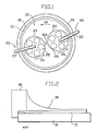
- the invention is carried out on a rotating polish wheel 10 having a circular polishing pad 12 mounted thereon.
- the polishing wheel 10 rotates in a direction indicated by arrow 14.
- the inventors have practiced the invention on a polish tool Model No. 6CU sold by the Strasbaugh Co. of Huntington Beach, CA.
- the wafers 28 to be planarized are held against the spinning polish wheel 10 by a quill assembly 20.
- the quill assembly includes a moveable support arm 22 for bringing the wafer 28 into contact with the polish pad 12, and a wafer support 24 that spins in a direction indicated by arrow 26.
- the wafer support 26 is rotated by a belt assembly (not shown) disposed within support arm 22.
- the support 24 has an elastomeric pad (not shown) disposed within it for receiving the wafer 28.
- the wafers 28 are polished by the action of the spinning support 24, the spinning pad 12, and the slurry pool 30 disposed therebetween.
- the spin speed of both the table 10 and the quill 20 is reduced from 120 RPM to 15-30 RPM.
- endpoint detection is facilitated.
- silicon is much less susceptible to polishing. This means that when the silicon surface rubs against the polish wheel, it produces a far greater amount of drag than does the oxide.
- the inventors have taken advantage of this phenomenon to provide an accurate endpoint detection method.
- a monitor (or dummy) wafer is included.
- the dummy wafer is a silicon substrate having the same amount of oxide on it as the amount of oxide on the product wafers to be removed by polishing.
- a pool of slurry is used in which the temperature is raised above room temperature, such that both polish rate uniformity and pad lifetime are maximized without promoting bumps.
Landscapes
- Engineering & Computer Science (AREA)
- Mechanical Engineering (AREA)
- Mechanical Treatment Of Semiconductor (AREA)
- Finish Polishing, Edge Sharpening, And Grinding By Specific Grinding Devices (AREA)
Applications Claiming Priority (2)
| Application Number | Priority Date | Filing Date | Title |
|---|---|---|---|
| US263842 | 1988-10-28 | ||
| US07/263,842 US4910155A (en) | 1988-10-28 | 1988-10-28 | Wafer flood polishing |
Publications (3)
| Publication Number | Publication Date |
|---|---|
| EP0366027A2 true EP0366027A2 (de) | 1990-05-02 |
| EP0366027A3 EP0366027A3 (de) | 1991-01-09 |
| EP0366027B1 EP0366027B1 (de) | 1993-09-15 |
Family
ID=23003463
Family Applications (1)
| Application Number | Title | Priority Date | Filing Date |
|---|---|---|---|
| EP89119566A Expired - Lifetime EP0366027B1 (de) | 1988-10-28 | 1989-10-21 | Polieren von Wafern in einem Flüssigkeitsbad |
Country Status (4)
| Country | Link |
|---|---|
| US (2) | US4910155A (de) |
| EP (1) | EP0366027B1 (de) |
| JP (1) | JPH077755B2 (de) |
| DE (1) | DE68909168T2 (de) |
Cited By (8)
| Publication number | Priority date | Publication date | Assignee | Title |
|---|---|---|---|---|
| DE4105145A1 (de) * | 1990-03-01 | 1991-09-05 | Intel Corp | Verfahren und vorrichtung zum planar-schleifen der oberflaeche eines dielektrikums, das auf einem halbleiter-substrat aufgebracht ist |
| EP0589434A1 (de) * | 1992-09-24 | 1994-03-30 | Ebara Corporation | Poliergerät |
| EP0624432A4 (de) * | 1992-10-30 | 1995-04-19 | Bbf Yamate Corp | Polierverfahren, hierzu bestimmte vorrichtung und schwabbel-/polierscheibe. |
| EP0739686A3 (de) * | 1995-04-25 | 1996-11-13 | AT&T IPM Corp. | Verfahren und Vorrichtung zum Polieren von metalllöslichen Materialen z.B. Diamant |
| EP0751205A2 (de) | 1995-06-29 | 1997-01-02 | Shell Internationale Researchmaatschappij B.V. | Verfahren zur Verwandlung von Rückstandskohlenwasserstoffölen |
| WO1997044160A1 (en) * | 1996-05-21 | 1997-11-27 | Micron Technology, Inc. | Method for chemical-mechanical planarization of stop-on-feature semiconductor wafers |
| US5957750A (en) * | 1997-12-18 | 1999-09-28 | Micron Technology, Inc. | Method and apparatus for controlling a temperature of a polishing pad used in planarizing substrates |
| KR100359070B1 (ko) * | 1998-10-13 | 2002-11-04 | 닛본 덴기 가부시끼가이샤 | 반도체 장치 제조방법 |
Families Citing this family (147)
| Publication number | Priority date | Publication date | Assignee | Title |
|---|---|---|---|---|
| US5399528A (en) * | 1989-06-01 | 1995-03-21 | Leibovitz; Jacques | Multi-layer fabrication in integrated circuit systems |
| US5191738A (en) * | 1989-06-16 | 1993-03-09 | Shin-Etsu Handotai Co., Ltd. | Method of polishing semiconductor wafer |
| US5094972A (en) * | 1990-06-14 | 1992-03-10 | National Semiconductor Corp. | Means of planarizing integrated circuits with fully recessed isolation dielectric |
| US5036015A (en) * | 1990-09-24 | 1991-07-30 | Micron Technology, Inc. | Method of endpoint detection during chemical/mechanical planarization of semiconductor wafers |
| US5064683A (en) * | 1990-10-29 | 1991-11-12 | Motorola, Inc. | Method for polish planarizing a semiconductor substrate by using a boron nitride polish stop |
| US5413966A (en) * | 1990-12-20 | 1995-05-09 | Lsi Logic Corporation | Shallow trench etch |
| US5290396A (en) * | 1991-06-06 | 1994-03-01 | Lsi Logic Corporation | Trench planarization techniques |
| JP3362397B2 (ja) * | 1991-03-28 | 2003-01-07 | ソニー株式会社 | ポリッシュによる平坦化工程を含む電子装置の製造方法 |
| US5069002A (en) * | 1991-04-17 | 1991-12-03 | Micron Technology, Inc. | Apparatus for endpoint detection during mechanical planarization of semiconductor wafers |
| US5128281A (en) * | 1991-06-05 | 1992-07-07 | Texas Instruments Incorporated | Method for polishing semiconductor wafer edges |
| US5225358A (en) * | 1991-06-06 | 1993-07-06 | Lsi Logic Corporation | Method of forming late isolation with polishing |
| US5248625A (en) * | 1991-06-06 | 1993-09-28 | Lsi Logic Corporation | Techniques for forming isolation structures |
| US5252503A (en) * | 1991-06-06 | 1993-10-12 | Lsi Logic Corporation | Techniques for forming isolation structures |
| US5320706A (en) * | 1991-10-15 | 1994-06-14 | Texas Instruments Incorporated | Removing slurry residue from semiconductor wafer planarization |
| US5308438A (en) * | 1992-01-30 | 1994-05-03 | International Business Machines Corporation | Endpoint detection apparatus and method for chemical/mechanical polishing |
| US5245790A (en) * | 1992-02-14 | 1993-09-21 | Lsi Logic Corporation | Ultrasonic energy enhanced chemi-mechanical polishing of silicon wafers |
| US5422289A (en) * | 1992-04-27 | 1995-06-06 | National Semiconductor Corporation | Method of manufacturing a fully planarized MOSFET and resulting structure |
| US5302551A (en) * | 1992-05-11 | 1994-04-12 | National Semiconductor Corporation | Method for planarizing the surface of an integrated circuit over a metal interconnect layer |
| US5445996A (en) * | 1992-05-26 | 1995-08-29 | Kabushiki Kaisha Toshiba | Method for planarizing a semiconductor device having a amorphous layer |
| US5265378A (en) * | 1992-07-10 | 1993-11-30 | Lsi Logic Corporation | Detecting the endpoint of chem-mech polishing and resulting semiconductor device |
| JPH0697132A (ja) * | 1992-07-10 | 1994-04-08 | Lsi Logic Corp | 半導体ウェハの化学機械的研磨装置、同装置のプラテンへの半導体ウェハ研磨用パッドの取付け方法、および同装置の研磨用複合パッド |
| US5310455A (en) * | 1992-07-10 | 1994-05-10 | Lsi Logic Corporation | Techniques for assembling polishing pads for chemi-mechanical polishing of silicon wafers |
| US5299393A (en) * | 1992-07-21 | 1994-04-05 | International Business Machines Corporation | Slurry containment device for polishing semiconductor wafers |
| US5466636A (en) * | 1992-09-17 | 1995-11-14 | International Business Machines Corporation | Method of forming borderless contacts using a removable mandrel |
| US5529936A (en) * | 1992-09-30 | 1996-06-25 | Lsi Logic Corporation | Method of etching a lens for a semiconductor solid state image sensor |
| US5340978A (en) * | 1992-09-30 | 1994-08-23 | Lsi Logic Corporation | Image-sensing display panels with LCD display panel and photosensitive element array |
| US5760834A (en) * | 1992-09-30 | 1998-06-02 | Lsi Logic | Electronic camera with binary lens element array |
| US5232875A (en) * | 1992-10-15 | 1993-08-03 | Micron Technology, Inc. | Method and apparatus for improving planarity of chemical-mechanical planarization operations |
| US5300155A (en) * | 1992-12-23 | 1994-04-05 | Micron Semiconductor, Inc. | IC chemical mechanical planarization process incorporating slurry temperature control |
| US5324690A (en) * | 1993-02-01 | 1994-06-28 | Motorola Inc. | Semiconductor device having a ternary boron nitride film and a method for forming the same |
| US5626715A (en) * | 1993-02-05 | 1997-05-06 | Lsi Logic Corporation | Methods of polishing semiconductor substrates |
| US5389194A (en) * | 1993-02-05 | 1995-02-14 | Lsi Logic Corporation | Methods of cleaning semiconductor substrates after polishing |
| US5532191A (en) * | 1993-03-26 | 1996-07-02 | Kawasaki Steel Corporation | Method of chemical mechanical polishing planarization of an insulating film using an etching stop |
| US5356513A (en) * | 1993-04-22 | 1994-10-18 | International Business Machines Corporation | Polishstop planarization method and structure |
| CA2169923A1 (en) * | 1993-09-17 | 1995-03-23 | Christopher R. Needham | Forming microlenses on solid state imager |
| US5395801A (en) * | 1993-09-29 | 1995-03-07 | Micron Semiconductor, Inc. | Chemical-mechanical polishing processes of planarizing insulating layers |
| US5643053A (en) * | 1993-12-27 | 1997-07-01 | Applied Materials, Inc. | Chemical mechanical polishing apparatus with improved polishing control |
| US5595522A (en) * | 1994-01-04 | 1997-01-21 | Texas Instruments Incorporated | Semiconductor wafer edge polishing system and method |
| US5422316A (en) * | 1994-03-18 | 1995-06-06 | Memc Electronic Materials, Inc. | Semiconductor wafer polisher and method |
| US5733175A (en) | 1994-04-25 | 1998-03-31 | Leach; Michael A. | Polishing a workpiece using equal velocity at all points overlapping a polisher |
| US5783497A (en) * | 1994-08-02 | 1998-07-21 | Sematech, Inc. | Forced-flow wafer polisher |
| US5562530A (en) * | 1994-08-02 | 1996-10-08 | Sematech, Inc. | Pulsed-force chemical mechanical polishing |
| US5607341A (en) | 1994-08-08 | 1997-03-04 | Leach; Michael A. | Method and structure for polishing a wafer during manufacture of integrated circuits |
| TW274625B (de) * | 1994-09-30 | 1996-04-21 | Hitachi Seisakusyo Kk | |
| US5527423A (en) * | 1994-10-06 | 1996-06-18 | Cabot Corporation | Chemical mechanical polishing slurry for metal layers |
| JP3637977B2 (ja) * | 1995-01-19 | 2005-04-13 | 株式会社荏原製作所 | ポリッシングの終点検知方法 |
| US5665201A (en) * | 1995-06-06 | 1997-09-09 | Advanced Micro Devices, Inc. | High removal rate chemical-mechanical polishing |
| KR970018240A (ko) * | 1995-09-08 | 1997-04-30 | 모리시다 요이치 | 반도체 기판의 연마방법 및 그 장치 |
| US5672095A (en) * | 1995-09-29 | 1997-09-30 | Intel Corporation | Elimination of pad conditioning in a chemical mechanical polishing process |
| US5840623A (en) * | 1995-10-04 | 1998-11-24 | Advanced Micro Devices, Inc. | Efficient and economical method of planarization of multilevel metallization structures in integrated circuits using CMP |
| US5709593A (en) | 1995-10-27 | 1998-01-20 | Applied Materials, Inc. | Apparatus and method for distribution of slurry in a chemical mechanical polishing system |
| JP3649493B2 (ja) * | 1995-11-02 | 2005-05-18 | 株式会社荏原製作所 | ポリッシングの終点決定方法及び装置 |
| US5726099A (en) * | 1995-11-07 | 1998-03-10 | International Business Machines Corporation | Method of chemically mechanically polishing an electronic component using a non-selective ammonium persulfate slurry |
| EP0779655A3 (de) * | 1995-12-14 | 1997-07-16 | International Business Machines Corporation | Verfahren zum chemisch-mechanischen Polieren eines Halbleitersubstrats eines elektronischen Bauteils |
| US5707492A (en) * | 1995-12-18 | 1998-01-13 | Motorola, Inc. | Metallized pad polishing process |
| US5618447A (en) * | 1996-02-13 | 1997-04-08 | Micron Technology, Inc. | Polishing pad counter meter and method for real-time control of the polishing rate in chemical-mechanical polishing of semiconductor wafers |
| KR0183826B1 (ko) * | 1996-03-04 | 1999-05-01 | 김광호 | 연마공정 후처리용 세정 용액 및 그를 이용하는 세정 방법 |
| JPH09321001A (ja) * | 1996-05-31 | 1997-12-12 | Komatsu Electron Metals Co Ltd | 半導体ウェハの研磨方法 |
| US5993686A (en) * | 1996-06-06 | 1999-11-30 | Cabot Corporation | Fluoride additive containing chemical mechanical polishing slurry and method for use of same |
| US5710069A (en) * | 1996-08-26 | 1998-01-20 | Motorola, Inc. | Measuring slurry particle size during substrate polishing |
| US6039891A (en) | 1996-09-24 | 2000-03-21 | Cabot Corporation | Multi-oxidizer precursor for chemical mechanical polishing |
| US6033596A (en) * | 1996-09-24 | 2000-03-07 | Cabot Corporation | Multi-oxidizer slurry for chemical mechanical polishing |
| US5783489A (en) * | 1996-09-24 | 1998-07-21 | Cabot Corporation | Multi-oxidizer slurry for chemical mechanical polishing |
| JP3788533B2 (ja) * | 1996-09-30 | 2006-06-21 | 東京エレクトロン株式会社 | 研磨装置および研磨方法 |
| US5972792A (en) * | 1996-10-18 | 1999-10-26 | Micron Technology, Inc. | Method for chemical-mechanical planarization of a substrate on a fixed-abrasive polishing pad |
| US6043206A (en) * | 1996-10-19 | 2000-03-28 | Samsung Electronics Co., Ltd. | Solutions for cleaning integrated circuit substrates |
| US6068787A (en) * | 1996-11-26 | 2000-05-30 | Cabot Corporation | Composition and slurry useful for metal CMP |
| US5958288A (en) * | 1996-11-26 | 1999-09-28 | Cabot Corporation | Composition and slurry useful for metal CMP |
| US5954997A (en) | 1996-12-09 | 1999-09-21 | Cabot Corporation | Chemical mechanical polishing slurry useful for copper substrates |
| US6126853A (en) * | 1996-12-09 | 2000-10-03 | Cabot Microelectronics Corporation | Chemical mechanical polishing slurry useful for copper substrates |
| US6309560B1 (en) | 1996-12-09 | 2001-10-30 | Cabot Microelectronics Corporation | Chemical mechanical polishing slurry useful for copper substrates |
| US6602439B1 (en) * | 1997-02-24 | 2003-08-05 | Superior Micropowders, Llc | Chemical-mechanical planarization slurries and powders and methods for using same |
| US5885135A (en) * | 1997-04-23 | 1999-03-23 | International Business Machines Corporation | CMP wafer carrier for preferential polishing of a wafer |
| US5873769A (en) * | 1997-05-30 | 1999-02-23 | Industrial Technology Research Institute | Temperature compensated chemical mechanical polishing to achieve uniform removal rates |
| US6030487A (en) * | 1997-06-19 | 2000-02-29 | International Business Machines Corporation | Wafer carrier assembly |
| US6099798A (en) * | 1997-10-31 | 2000-08-08 | Nanogram Corp. | Ultraviolet light block and photocatalytic materials |
| US6726990B1 (en) | 1998-05-27 | 2004-04-27 | Nanogram Corporation | Silicon oxide particles |
| US20060147369A1 (en) * | 1997-07-21 | 2006-07-06 | Neophotonics Corporation | Nanoparticle production and corresponding structures |
| US6290735B1 (en) | 1997-10-31 | 2001-09-18 | Nanogram Corporation | Abrasive particles for surface polishing |
| US7384680B2 (en) * | 1997-07-21 | 2008-06-10 | Nanogram Corporation | Nanoparticle-based power coatings and corresponding structures |
| US20090255189A1 (en) * | 1998-08-19 | 2009-10-15 | Nanogram Corporation | Aluminum oxide particles |
| US20090075083A1 (en) * | 1997-07-21 | 2009-03-19 | Nanogram Corporation | Nanoparticle production and corresponding structures |
| US5997392A (en) * | 1997-07-22 | 1999-12-07 | International Business Machines Corporation | Slurry injection technique for chemical-mechanical polishing |
| US6099604A (en) * | 1997-08-21 | 2000-08-08 | Micron Technology, Inc. | Slurry with chelating agent for chemical-mechanical polishing of a semiconductor wafer and methods related thereto |
| US6069095A (en) * | 1997-08-22 | 2000-05-30 | Texas Instruments Incorporated | Ultra-clean wafer chuck assembly for moisture-sensitive processes conducted in rapid thermal processors |
| US6102784A (en) * | 1997-11-05 | 2000-08-15 | Speedfam-Ipec Corporation | Method and apparatus for improved gear cleaning assembly in polishing machines |
| US6336845B1 (en) | 1997-11-12 | 2002-01-08 | Lam Research Corporation | Method and apparatus for polishing semiconductor wafers |
| US6146241A (en) * | 1997-11-12 | 2000-11-14 | Fujitsu Limited | Apparatus for uniform chemical mechanical polishing by intermittent lifting and reversible rotation |
| KR100286980B1 (ko) * | 1998-02-11 | 2001-04-16 | 윤종용 | 웨이퍼 연마 설비 및 웨이퍼 연마 방법 |
| US6114249A (en) * | 1998-03-10 | 2000-09-05 | International Business Machines Corporation | Chemical mechanical polishing of multiple material substrates and slurry having improved selectivity |
| US6432828B2 (en) | 1998-03-18 | 2002-08-13 | Cabot Microelectronics Corporation | Chemical mechanical polishing slurry useful for copper substrates |
| US6019665A (en) * | 1998-04-30 | 2000-02-01 | Fujitsu Limited | Controlled retention of slurry in chemical mechanical polishing |
| KR100548750B1 (ko) * | 1998-04-30 | 2006-02-06 | 더 비오씨 그룹, 인크. | 슬러리 혼합용 전도율 귀환 제어 시스템 |
| US6210257B1 (en) * | 1998-05-29 | 2001-04-03 | Micron Technology, Inc. | Web-format polishing pads and methods for manufacturing and using web-format polishing pads in mechanical and chemical-mechanical planarization of microelectronic substrates |
| US5944588A (en) * | 1998-06-25 | 1999-08-31 | International Business Machines Corporation | Chemical mechanical polisher |
| US6063306A (en) * | 1998-06-26 | 2000-05-16 | Cabot Corporation | Chemical mechanical polishing slurry useful for copper/tantalum substrate |
| US6217416B1 (en) | 1998-06-26 | 2001-04-17 | Cabot Microelectronics Corporation | Chemical mechanical polishing slurry useful for copper/tantalum substrates |
| US6558570B2 (en) | 1998-07-01 | 2003-05-06 | Micron Technology, Inc. | Polishing slurry and method for chemical-mechanical polishing |
| US6220934B1 (en) | 1998-07-23 | 2001-04-24 | Micron Technology, Inc. | Method for controlling pH during planarization and cleaning of microelectronic substrates |
| US6129610A (en) * | 1998-08-14 | 2000-10-10 | International Business Machines Corporation | Polish pressure modulation in CMP to preferentially polish raised features |
| US5972787A (en) * | 1998-08-18 | 1999-10-26 | International Business Machines Corp. | CMP process using indicator areas to determine endpoint |
| SG99289A1 (en) * | 1998-10-23 | 2003-10-27 | Ibm | Chemical-mechanical planarization of metallurgy |
| US6261158B1 (en) | 1998-12-16 | 2001-07-17 | Speedfam-Ipec | Multi-step chemical mechanical polishing |
| JP2000216120A (ja) * | 1999-01-27 | 2000-08-04 | Mitsubishi Electric Corp | 研磨装置およびこれを用いた半導体装置の製造方法 |
| US6491570B1 (en) | 1999-02-25 | 2002-12-10 | Applied Materials, Inc. | Polishing media stabilizer |
| US6066030A (en) * | 1999-03-04 | 2000-05-23 | International Business Machines Corporation | Electroetch and chemical mechanical polishing equipment |
| US6213846B1 (en) | 1999-07-12 | 2001-04-10 | International Business Machines Corporation | Real-time control of chemical-mechanical polishing processes using a shaft distortion measurement |
| US6343975B1 (en) | 1999-10-05 | 2002-02-05 | Peter Mok | Chemical-mechanical polishing apparatus with circular motion pads |
| US6431959B1 (en) * | 1999-12-20 | 2002-08-13 | Lam Research Corporation | System and method of defect optimization for chemical mechanical planarization of polysilicon |
| US6186873B1 (en) | 2000-04-14 | 2001-02-13 | International Business Machines Corporation | Wafer edge cleaning |
| US6561884B1 (en) | 2000-08-29 | 2003-05-13 | Applied Materials, Inc. | Web lift system for chemical mechanical planarization |
| US6592439B1 (en) | 2000-11-10 | 2003-07-15 | Applied Materials, Inc. | Platen for retaining polishing material |
| CN1255854C (zh) * | 2001-01-16 | 2006-05-10 | 卡伯特微电子公司 | 含有草酸铵的抛光系统及方法 |
| US6383065B1 (en) | 2001-01-22 | 2002-05-07 | Cabot Microelectronics Corporation | Catalytic reactive pad for metal CMP |
| US6799136B2 (en) * | 2001-08-09 | 2004-09-28 | Texas Instruments Incorporated | Method of estimation of wafer polish rates |
| US6503131B1 (en) | 2001-08-16 | 2003-01-07 | Applied Materials, Inc. | Integrated platen assembly for a chemical mechanical planarization system |
| US6458020B1 (en) * | 2001-11-16 | 2002-10-01 | International Business Machines Corporation | Slurry recirculation in chemical mechanical polishing |
| KR100444721B1 (ko) * | 2001-12-20 | 2004-08-16 | 동부전자 주식회사 | 금속배선 전 절연막의 평탄화 방법 |
| US7004819B2 (en) | 2002-01-18 | 2006-02-28 | Cabot Microelectronics Corporation | CMP systems and methods utilizing amine-containing polymers |
| US20030162398A1 (en) | 2002-02-11 | 2003-08-28 | Small Robert J. | Catalytic composition for chemical-mechanical polishing, method of using same, and substrate treated with same |
| US7964005B2 (en) * | 2003-04-10 | 2011-06-21 | Technion Research & Development Foundation Ltd. | Copper CMP slurry composition |
| US7001827B2 (en) * | 2003-04-15 | 2006-02-21 | International Business Machines Corporation | Semiconductor wafer front side protection |
| US6939200B2 (en) * | 2003-09-16 | 2005-09-06 | Hitachi Global Storage Technologies Netherlands B.V. | Method of predicting plate lapping properties to improve slider fabrication yield |
| US6918815B2 (en) * | 2003-09-16 | 2005-07-19 | Hitachi Global Storage Technologies Netherlands B.V. | System and apparatus for predicting plate lapping properties to improve slider fabrication yield |
| US7255810B2 (en) * | 2004-01-09 | 2007-08-14 | Cabot Microelectronics Corporation | Polishing system comprising a highly branched polymer |
| US6971945B2 (en) * | 2004-02-23 | 2005-12-06 | Rohm And Haas Electronic Materials Cmp Holdings, Inc. | Multi-step polishing solution for chemical mechanical planarization |
| US20050206007A1 (en) * | 2004-03-18 | 2005-09-22 | Lei Li | Structure and method for contact pads having a recessed bondable metal plug over of copper-metallized integrated circuits |
| US7232363B2 (en) * | 2004-07-22 | 2007-06-19 | Applied Materials, Inc. | Polishing solution retainer |
| US8038752B2 (en) | 2004-10-27 | 2011-10-18 | Cabot Microelectronics Corporation | Metal ion-containing CMP composition and method for using the same |
| US7803203B2 (en) | 2005-09-26 | 2010-09-28 | Cabot Microelectronics Corporation | Compositions and methods for CMP of semiconductor materials |
| KR100710804B1 (ko) * | 2006-02-03 | 2007-04-23 | 삼성전자주식회사 | 반도체 소자의 평탄화 방법 |
| JP4814677B2 (ja) * | 2006-03-31 | 2011-11-16 | 株式会社荏原製作所 | 基板保持装置および研磨装置 |
| US8759216B2 (en) | 2006-06-07 | 2014-06-24 | Cabot Microelectronics Corporation | Compositions and methods for polishing silicon nitride materials |
| US20080220610A1 (en) * | 2006-06-29 | 2008-09-11 | Cabot Microelectronics Corporation | Silicon oxide polishing method utilizing colloidal silica |
| US8197306B2 (en) * | 2008-10-31 | 2012-06-12 | Araca, Inc. | Method and device for the injection of CMP slurry |
| US8845395B2 (en) | 2008-10-31 | 2014-09-30 | Araca Inc. | Method and device for the injection of CMP slurry |
| US8602842B2 (en) * | 2010-03-12 | 2013-12-10 | Wayne O. Duescher | Three-point fixed-spindle floating-platen abrasive system |
| US8500515B2 (en) * | 2010-03-12 | 2013-08-06 | Wayne O. Duescher | Fixed-spindle and floating-platen abrasive system using spherical mounts |
| US8740668B2 (en) * | 2010-03-12 | 2014-06-03 | Wayne O. Duescher | Three-point spindle-supported floating abrasive platen |
| US8647171B2 (en) * | 2010-03-12 | 2014-02-11 | Wayne O. Duescher | Fixed-spindle floating-platen workpiece loader apparatus |
| CN102172885B (zh) * | 2011-01-31 | 2013-05-15 | 北京通美晶体技术有限公司 | 衬底的抛光装置及其抛光的衬底 |
| US9358660B2 (en) | 2011-11-07 | 2016-06-07 | Taiwan Semiconductor Manufacturing Company, Ltd. | Grinding wheel design with elongated teeth arrangement |
| US9960088B2 (en) | 2011-11-07 | 2018-05-01 | Taiwan Semiconductor Manufacturing Company, Ltd. | End point detection in grinding |
| US9633863B2 (en) | 2012-07-11 | 2017-04-25 | Cabot Microelectronics Corporation | Compositions and methods for selective polishing of silicon nitride materials |
| US9828574B2 (en) | 2015-01-13 | 2017-11-28 | Cabot Microelectronics Corporation | Cleaning composition and method for cleaning semiconductor wafers after CMP |
| US11077536B2 (en) | 2016-06-24 | 2021-08-03 | Applied Materials, Inc. | Slurry distribution device for chemical mechanical polishing |
| CN107030589A (zh) * | 2017-03-14 | 2017-08-11 | 黄河科技学院 | 一种化学机械研磨设备 |
Family Cites Families (31)
| Publication number | Priority date | Publication date | Assignee | Title |
|---|---|---|---|---|
| DE147589C (de) | ||||
| US2476851A (en) * | 1945-04-21 | 1949-07-19 | Honeywell Regulator Co | Motor control apparatus |
| US2922264A (en) * | 1955-02-01 | 1960-01-26 | Syntron Co | Method of lapping |
| DE1216651B (de) * | 1963-03-28 | 1966-05-12 | Siemens Ag | Verfahren zum polierenden Abtragen von einkristallinen Halbleiterkoerpern, insbesondere Halbleiterscheiben |
| US3342652A (en) * | 1964-04-02 | 1967-09-19 | Ibm | Chemical polishing of a semi-conductor substrate |
| US3615955A (en) * | 1969-02-28 | 1971-10-26 | Ibm | Method for polishing a silicon surface |
| US3841031A (en) * | 1970-10-21 | 1974-10-15 | Monsanto Co | Process for polishing thin elements |
| JPS545160A (en) * | 1977-06-14 | 1979-01-16 | Akira Washida | Shaft sealing device |
| US4561214A (en) * | 1978-10-12 | 1985-12-31 | Inoue-Japax Research Incorporated | Abrading tool |
| DD147589A1 (de) * | 1979-12-03 | 1981-04-08 | Bernd Nippe | Polierverfahren fuer halbleiteroberflaechen |
| US4256535A (en) * | 1979-12-05 | 1981-03-17 | Western Electric Company, Inc. | Method of polishing a semiconductor wafer |
| US4407094A (en) * | 1981-11-03 | 1983-10-04 | Transat Corp. | Apparatus for automatic lapping control |
| US4373991A (en) * | 1982-01-28 | 1983-02-15 | Western Electric Company, Inc. | Methods and apparatus for polishing a semiconductor wafer |
| US4524477A (en) * | 1984-05-21 | 1985-06-25 | U.S. Floor Systems, Inc. | Cleaning solution dispenser attachment for rotary floor cleaning machine |
| DE3421127A1 (de) * | 1984-06-07 | 1985-12-12 | Telefunken electronic GmbH, 7100 Heilbronn | Verfahren zum herstellen einer halbleiteranordnung |
| JPS61120424A (ja) * | 1984-11-16 | 1986-06-07 | Oki Electric Ind Co Ltd | 誘電体分離基板の研磨方法 |
| US4944836A (en) | 1985-10-28 | 1990-07-31 | International Business Machines Corporation | Chem-mech polishing method for producing coplanar metal/insulator films on a substrate |
| US4702792A (en) * | 1985-10-28 | 1987-10-27 | International Business Machines Corporation | Method of forming fine conductive lines, patterns and connectors |
| US4671851A (en) * | 1985-10-28 | 1987-06-09 | International Business Machines Corporation | Method for removing protuberances at the surface of a semiconductor wafer using a chem-mech polishing technique |
| US4757566A (en) * | 1987-07-27 | 1988-07-19 | Tennant Company | Control of torque in floor maintenance tools by drive motor load |
| US4956313A (en) | 1987-08-17 | 1990-09-11 | International Business Machines Corporation | Via-filling and planarization technique |
| JPS6487153A (en) * | 1987-09-22 | 1989-03-31 | Toshiba Machine Co Ltd | Grinding amount correction system for numerical control machine tool |
| JPH07115286B2 (ja) * | 1988-09-28 | 1995-12-13 | 愛晃エンジニアリング 株式会社 | 溶接余盛の自動研削装置 |
| JPH02124261A (ja) * | 1988-10-28 | 1990-05-11 | Kawasaki Steel Corp | 研磨量自動制御方法 |
| US5213655A (en) * | 1990-05-16 | 1993-05-25 | International Business Machines Corporation | Device and method for detecting an end point in polishing operation |
| US5290396A (en) * | 1991-06-06 | 1994-03-01 | Lsi Logic Corporation | Trench planarization techniques |
| JPH04343663A (ja) * | 1991-01-24 | 1992-11-30 | Shin Etsu Handotai Co Ltd | 円筒研削装置 |
| US5217566A (en) * | 1991-06-06 | 1993-06-08 | Lsi Logic Corporation | Densifying and polishing glass layers |
| US5308438A (en) * | 1992-01-30 | 1994-05-03 | International Business Machines Corporation | Endpoint detection apparatus and method for chemical/mechanical polishing |
| US5250897A (en) * | 1992-05-07 | 1993-10-05 | Lsi Logic Corporation | Solenoid/slug gap measurement tool for semiconductor equipment and method of measurement |
| US5234868A (en) * | 1992-10-29 | 1993-08-10 | International Business Machines Corporation | Method for determining planarization endpoint during chemical-mechanical polishing |
-
1988
- 1988-10-28 US US07/263,842 patent/US4910155A/en not_active Ceased
-
1989
- 1989-10-21 EP EP89119566A patent/EP0366027B1/de not_active Expired - Lifetime
- 1989-10-21 DE DE89119566T patent/DE68909168T2/de not_active Expired - Fee Related
- 1989-10-25 JP JP1276182A patent/JPH077755B2/ja not_active Expired - Fee Related
-
1992
- 1992-03-16 US US07/852,432 patent/USRE38029E1/en not_active Expired - Lifetime
Cited By (16)
| Publication number | Priority date | Publication date | Assignee | Title |
|---|---|---|---|---|
| DE4105145C2 (de) * | 1990-03-01 | 1998-07-02 | Intel Corp | Verfahren und Vorrichtung zum Planarisieren der Oberfläche eines Dielektrikums |
| DE4105145A1 (de) * | 1990-03-01 | 1991-09-05 | Intel Corp | Verfahren und vorrichtung zum planar-schleifen der oberflaeche eines dielektrikums, das auf einem halbleiter-substrat aufgebracht ist |
| EP0589434A1 (de) * | 1992-09-24 | 1994-03-30 | Ebara Corporation | Poliergerät |
| US5384986A (en) * | 1992-09-24 | 1995-01-31 | Ebara Corporation | Polishing apparatus |
| USRE38228E1 (en) * | 1992-09-24 | 2003-08-19 | Ebara Corporation | Polishing apparatus |
| EP0624432A4 (de) * | 1992-10-30 | 1995-04-19 | Bbf Yamate Corp | Polierverfahren, hierzu bestimmte vorrichtung und schwabbel-/polierscheibe. |
| US5846122A (en) * | 1995-04-25 | 1998-12-08 | Lucent Technologies Inc. | Method and apparatus for polishing metal-soluble materials such as diamond |
| EP0739686A3 (de) * | 1995-04-25 | 1996-11-13 | AT&T IPM Corp. | Verfahren und Vorrichtung zum Polieren von metalllöslichen Materialen z.B. Diamant |
| EP0751205A2 (de) | 1995-06-29 | 1997-01-02 | Shell Internationale Researchmaatschappij B.V. | Verfahren zur Verwandlung von Rückstandskohlenwasserstoffölen |
| WO1997044160A1 (en) * | 1996-05-21 | 1997-11-27 | Micron Technology, Inc. | Method for chemical-mechanical planarization of stop-on-feature semiconductor wafers |
| US5893754A (en) * | 1996-05-21 | 1999-04-13 | Micron Technology, Inc. | Method for chemical-mechanical planarization of stop-on-feature semiconductor wafers |
| US5957750A (en) * | 1997-12-18 | 1999-09-28 | Micron Technology, Inc. | Method and apparatus for controlling a temperature of a polishing pad used in planarizing substrates |
| US6533647B1 (en) | 1997-12-18 | 2003-03-18 | Micron Technology, Inc. | Method for controlling a selected temperature of a planarizing surface of a polish pad. |
| US6682404B2 (en) | 1997-12-18 | 2004-01-27 | Micron Technology, Inc. | Method for controlling a temperature of a polishing pad used in planarizing substrates |
| US6837773B2 (en) | 1997-12-18 | 2005-01-04 | Micron Technology, Inc. | Method and apparatus for controlling a temperature of a polishing pad used in planarizing substrates |
| KR100359070B1 (ko) * | 1998-10-13 | 2002-11-04 | 닛본 덴기 가부시끼가이샤 | 반도체 장치 제조방법 |
Also Published As
| Publication number | Publication date |
|---|---|
| JPH077755B2 (ja) | 1995-01-30 |
| DE68909168D1 (de) | 1993-10-21 |
| EP0366027B1 (de) | 1993-09-15 |
| JPH02156635A (ja) | 1990-06-15 |
| EP0366027A3 (de) | 1991-01-09 |
| USRE38029E1 (en) | 2003-03-11 |
| DE68909168T2 (de) | 1994-04-21 |
| US4910155A (en) | 1990-03-20 |
Similar Documents
| Publication | Publication Date | Title |
|---|---|---|
| EP0366027B1 (de) | Polieren von Wafern in einem Flüssigkeitsbad | |
| US4879258A (en) | Integrated circuit planarization by mechanical polishing | |
| US5321304A (en) | Detecting the endpoint of chem-mech polishing, and resulting semiconductor device | |
| KR100489458B1 (ko) | 기판의 기계-화학적 평탄화 방법 | |
| US6423640B1 (en) | Headless CMP process for oxide planarization | |
| US7132035B2 (en) | Methods, apparatuses, and substrate assembly structures for fabricating microelectronic components using mechanical and chemical-mechanical planarization processes | |
| US6830500B2 (en) | Slurry for use with fixed-abrasive polishing pads in polishing semiconductor device conductive structures that include copper and tungsten and polishing methods | |
| KR100259936B1 (ko) | 연마제 | |
| EP0986097B1 (de) | Verfahren zur Rückgewinnung von Substratscheiben | |
| US7070480B2 (en) | Method and apparatus for polishing substrates | |
| JP3230986B2 (ja) | ポリッシング方法、半導体装置の製造方法及び半導体製造装置。 | |
| JP2003514061A (ja) | 誘電性CMPスラリーにおけるCsOHの使用 | |
| KR100578596B1 (ko) | 화학기계적 연마용 슬러리 조성물, 이를 이용한반도체소자의 표면 평탄화 방법 및 슬러리 조성물의선택비 제어방법 | |
| WO2000030159A1 (en) | Method to decrease dishing rate during cmp in metal semiconductor structures | |
| US6077147A (en) | Chemical-mechanical polishing station with end-point monitoring device | |
| US20020023719A1 (en) | Method and apparatus for removing a material layer from a substrate | |
| US6300247B2 (en) | Preconditioning polishing pads for chemical-mechanical polishing | |
| US6443807B1 (en) | Polishing process for use in method of fabricating semiconductor device | |
| US6489243B2 (en) | Method for polishing semiconductor device | |
| US6913525B2 (en) | CMP device and production method for semiconductor device | |
| US6875322B1 (en) | Electrochemical assisted CMP | |
| US6268224B1 (en) | Method and apparatus for detecting an ion-implanted polishing endpoint layer within a semiconductor wafer | |
| JP2004128112A (ja) | 半導体装置の製造方法 | |
| CN100369212C (zh) | Cmp研磨方法和半导体器件制造方法 | |
| US20070235345A1 (en) | Polishing method that suppresses hillock formation |
Legal Events
| Date | Code | Title | Description |
|---|---|---|---|
| PUAI | Public reference made under article 153(3) epc to a published international application that has entered the european phase |
Free format text: ORIGINAL CODE: 0009012 |
|
| AK | Designated contracting states |
Kind code of ref document: A2 Designated state(s): DE FR GB |
|
| 17P | Request for examination filed |
Effective date: 19900820 |
|
| PUAL | Search report despatched |
Free format text: ORIGINAL CODE: 0009013 |
|
| AK | Designated contracting states |
Kind code of ref document: A3 Designated state(s): DE FR GB |
|
| 17Q | First examination report despatched |
Effective date: 19920313 |
|
| GRAA | (expected) grant |
Free format text: ORIGINAL CODE: 0009210 |
|
| AK | Designated contracting states |
Kind code of ref document: B1 Designated state(s): DE FR GB |
|
| REF | Corresponds to: |
Ref document number: 68909168 Country of ref document: DE Date of ref document: 19931021 |
|
| ET | Fr: translation filed | ||
| PLBE | No opposition filed within time limit |
Free format text: ORIGINAL CODE: 0009261 |
|
| STAA | Information on the status of an ep patent application or granted ep patent |
Free format text: STATUS: NO OPPOSITION FILED WITHIN TIME LIMIT |
|
| 26N | No opposition filed | ||
| PGFP | Annual fee paid to national office [announced via postgrant information from national office to epo] |
Ref country code: DE Payment date: 19951030 Year of fee payment: 7 |
|
| PG25 | Lapsed in a contracting state [announced via postgrant information from national office to epo] |
Ref country code: DE Effective date: 19970701 |
|
| PGFP | Annual fee paid to national office [announced via postgrant information from national office to epo] |
Ref country code: FR Payment date: 19991018 Year of fee payment: 11 |
|
| PG25 | Lapsed in a contracting state [announced via postgrant information from national office to epo] |
Ref country code: FR Free format text: LAPSE BECAUSE OF NON-PAYMENT OF DUE FEES Effective date: 20010629 |
|
| REG | Reference to a national code |
Ref country code: FR Ref legal event code: ST |
|
| PGFP | Annual fee paid to national office [announced via postgrant information from national office to epo] |
Ref country code: GB Payment date: 20011001 Year of fee payment: 13 |
|
| REG | Reference to a national code |
Ref country code: GB Ref legal event code: IF02 |
|
| PG25 | Lapsed in a contracting state [announced via postgrant information from national office to epo] |
Ref country code: GB Free format text: LAPSE BECAUSE OF NON-PAYMENT OF DUE FEES Effective date: 20021021 |
|
| GBPC | Gb: european patent ceased through non-payment of renewal fee |
Effective date: 20021021 |