EP0366489A2 - NAND Gateschaltungen - Google Patents
NAND Gateschaltungen Download PDFInfo
- Publication number
- EP0366489A2 EP0366489A2 EP89311123A EP89311123A EP0366489A2 EP 0366489 A2 EP0366489 A2 EP 0366489A2 EP 89311123 A EP89311123 A EP 89311123A EP 89311123 A EP89311123 A EP 89311123A EP 0366489 A2 EP0366489 A2 EP 0366489A2
- Authority
- EP
- European Patent Office
- Prior art keywords
- nand gate
- driving
- transistors
- gate circuit
- transistor
- Prior art date
- Legal status (The legal status is an assumption and is not a legal conclusion. Google has not performed a legal analysis and makes no representation as to the accuracy of the status listed.)
- Granted
Links
Images


Classifications
-
- H—ELECTRICITY
- H03—ELECTRONIC CIRCUITRY
- H03K—PULSE TECHNIQUE
- H03K19/00—Logic circuits, i.e. having at least two inputs acting on one output; Inverting circuits
- H03K19/20—Logic circuits, i.e. having at least two inputs acting on one output; Inverting circuits characterised by logic function, e.g. AND, OR, NOR, NOT circuits
-
- H—ELECTRICITY
- H03—ELECTRONIC CIRCUITRY
- H03K—PULSE TECHNIQUE
- H03K19/00—Logic circuits, i.e. having at least two inputs acting on one output; Inverting circuits
- H03K19/003—Modifications for increasing the reliability for protection
- H03K19/00346—Modifications for eliminating interference or parasitic voltages or currents
- H03K19/00361—Modifications for eliminating interference or parasitic voltages or currents in field effect transistor circuits
-
- H—ELECTRICITY
- H03—ELECTRONIC CIRCUITRY
- H03K—PULSE TECHNIQUE
- H03K19/00—Logic circuits, i.e. having at least two inputs acting on one output; Inverting circuits
- H03K19/02—Logic circuits, i.e. having at least two inputs acting on one output; Inverting circuits using specified components
- H03K19/08—Logic circuits, i.e. having at least two inputs acting on one output; Inverting circuits using specified components using semiconductor devices
- H03K19/094—Logic circuits, i.e. having at least two inputs acting on one output; Inverting circuits using specified components using semiconductor devices using field-effect transistors
- H03K19/0944—Logic circuits, i.e. having at least two inputs acting on one output; Inverting circuits using specified components using semiconductor devices using field-effect transistors using MOSFET or insulated gate field-effect transistors, i.e. IGFET
- H03K19/09441—Logic circuits, i.e. having at least two inputs acting on one output; Inverting circuits using specified components using semiconductor devices using field-effect transistors using MOSFET or insulated gate field-effect transistors, i.e. IGFET of the same canal type
- H03K19/09443—Logic circuits, i.e. having at least two inputs acting on one output; Inverting circuits using specified components using semiconductor devices using field-effect transistors using MOSFET or insulated gate field-effect transistors, i.e. IGFET of the same canal type using a combination of enhancement and depletion transistors
Definitions
- the present invention relates to NAND gate circuits, for example for use in decoder circuits provided in semiconductor memory devices.
- Figure 1(A) shows an ordinary conventional decoder circuit and in Fig. 1 V cc is a source voltage, for example 5 V, while V ss is a ground potential (0 V).
- a transistor T1 used for a load means, for example, an N channel depletion type MOS transistor, and driving transistors T2 and T3 , for example, N channel enhancement type MOS transistors used as a driving circuit, are provided.
- both an input a to the transistor T2 and an input b to the transistor T3 are binary signals and the transistors T2 and T3 are of the same type.
- the output voltage V OUT changes from a voltage of nearly 5 V to nearly 0 V or from nearly 0 V to nearly 5 V.
- the level of the voltage should be discriminated as "H”, and when the voltage is lower than 2 V, it should be discriminated as "L”, the output level of the NAND gate circuit should change from “H” to "L” when the voltage of the input b reaches 2V as it is increased from 0 V to 5 V.
- the input voltage at which the level of the output voltage of the NAND gate circuit changes from “H” to “L” or vice versa is called the input threshold voltage of the NAND gate circuit.
- the input threshold voltage changes depending upon the respective values of the input voltages applied to the inputs a and b at any one time.
- the input threshold voltage of the NAND gate circuit differs as shown in Fig. 1(B), in three ways depending on whether the input voltage b was changed while the input voltage a was fixed at 5 V (only the input voltage b was changed) as shown by a curve (2) in Fig. 1(B), the input voltage a was changed while the input voltage b was fixed at 5 V (only the input voltage a was changed) as shown by a curve (1) in Fig. 1(B), or both the input voltages a and b were simultaneously changed (both the input voltages a and b are changed) as shown by a curve (3) in Fig. 1(B).
- the input threshold voltage of the NAND gate circuit obtained when only the input voltage b is changed and the input voltage a is fixed at 5 V is 1.5 V
- the input threshold voltage obtained when the input voltage a is changed and the input voltage b is fixed at 5 V is 2.0 V
- the input threshold voltage obtained when both the input voltages a and b are simultaneously changed is 2.5 V.
- the source voltage of the transistor T3 is V SS , i.e. 0 V.
- the drain voltage of the transistor T3 is initially above 0 V due to the transistor T3 being ON, enabling current to flow therein.
- the source voltage of the transistor T2 is thus initially also above V ss , i.e. 0 V since the drain voltage of the transistor T3 corresponds to the source voltage of the transistor T2.
- the gate-source voltage of the transistor T2 is reduced at that time. Therefore, the output of the NAND gate circuit cannot be changed unless a relatively high voltage is applied to the input a of the transistor T2.
- the threshold voltage of the NAND gate circuit will be substantially increased since the total current driving performance of each transistor T2 and T3 is weakened compared with the performance obtained in the situation in which one of the input voltages a and b is fixed at 5 V.
- the threshold voltage of the NAND gate circuit changes according to the combination of the input voltages applied to the input terminals of the circuit, a problem arises in that the noise immunity, i.e. the immunity to noise, for a particular signal input to a certain transistor can become different from the others and the total noise immunity can deteriorate accordingly.
- the noise immunity i.e. the immunity to noise
- the transistors used in the NAND gate circuit may have the following characteristics, for example.
- the transistors T2 and T3 have a threshold voltage V th of 0.6 V, a gate oxide film thickness of 350 ⁇ , a gate width of 50 ⁇ m, and a gate length of 2 ⁇ m, while the transistor T1 has a threshold voltage V th of -3.5 V, a gate oxide film thickness of 350 ⁇ , a gate width of 20 ⁇ m, and a gate length of 5 ⁇ m.
- the input threshold voltages are 2.15 V, 1.95 V and 2.45 V in the cases when the input voltage a alone is changed, the input voltage b alone is changed and both the input voltages a and b are simultaneously changed, respectively.
- the curves (1), (2), and (3) show respective input-output characteristics of the NAND gate circuit in the above-mentioned three cases.
- the NAND gate circuit outputs a voltage having a level of "H” instead of "L” when noise is added to any one of the input signals to reduce the input signal voltage level below 2.55 V.
- Such a NAND gate circuit will frequently operate erroneously with respect to the signals input to the gates of the driving transistors of the driving circuit. Since the NAND gate circuit is generally used for a main circuit of a decoder connected to a memory cell array in a memory device, when the NAND gate circuit erroneously operates due to noise added to the signals, input to the gates of the driving transistors, the erroneous information generated from the NAND gate circuit, i.e., decoder, significantly affects the memory cell array or the like in the memory device, causing erroneous information to be output from the memory device.
- One type of decoder including a NAND gate circuit has a circuit construction as shown in Fig. 2, and is known from Japanese Unexamined Patent Publication (Kokai) No. 61-45496.
- a voltage source V PPI in a decoder circuit consisting of NAND gate circuit, can be internally switched to two different voltage levels such as a low voltage of about 5 V (referred to as V cc hereinafter) in a reading mode and a high voltage of about 12.5 V (referred to as V PP hereinafter) in a writing mode.
- V cc low voltage of about 5 V
- V PP high voltage of about 12.5 V
- the decoder includes a decoder circuit and a CMOS inverter (IV).
- an N-channel depletion type MOS transistor T1 and N-channel enhancement type MOS transistors T2 to T5 are provided.
- an N-channel enhancement type MOS transistor T7 and a P channel enhancement type MOS transistor T6 are provided.
- the NAND gate circuit consists of the transistor T1 as a load means and the transistors T2 to T5 as a driving circuit.
- the output N1 which drives the CMOS inverter (IV) consists of the transistors T6 and T7.
- An output of the CMOS inverter (IV) connects to a word line (WL).
- a memory cell transistor MC is provided at each cross point of the word line (WL) and bit lines BL0 , BL1 , BL2 .
- Input address signals a to d are applied to the gates of the driving transistors T2 to T5 , respectively.
- these input address signals selectively are at either the V cc level (logic "1") or V ss level (logic "0", usually denoting ground level, i.e., 0 V).
- the node N1 (output of the decoder circuit) is reduced nearly to V ss , i.e., 0 V, regardless of whether the decoder source voltage V PPI is V cc or V PP .
- the node N2 i.e., the output voltage of the inverter is increased to V PPI .
- the output N1 of the decoder circuit (DEC) is increased to V PPI .
- V ss i.e., 0 V.
- the input address signals a to d are derived from, for example, the outputs of an address buffer circuit in which the address signals applied externally thereto are subjected to a waveform shaping operation inside the chip.
- address signal inputs externally provided are applied to the input terminal of a buffer circuit with a waveform as shown in Fig. 3(a), are subjected to a waveform shaping operation, and are output to the input terminals of the decoder circuit with a waveform as shown in Fig. 3(b).
- the decoder will erroneously operate depending upon the level of the abnormal signal portion and the level of the threshold set for the decoder circuit.
- the decoder circuit will erroneously operate and output a erroneous signal information Z to the word line WL as shown in Fig. 3(c).
- the input threshold voltage is set at 1.5 V.
- the word line WL connected to this decoder is a non-selected word line and thereby the signal level thereof inherently is "L", although the level of the word line will be increased from the level of 0 V to form an abnormal signal portion z as shown in Fig. 3(c) so as to mistakenly read or write information from or into a certain memory cell.
- a plurality of pairs of resistors and capacitors are serially arranged therein.
- a signal output from an inventor including an abnormal signal level will be delayed and the duration of the abnormal signal portion will be prolonged due to the existence of the plurality of time constants created by CR.
- the sense amplifier When such a prolonged signal portion p is output to the sense amplifier, the sense amplifier will necessarily read erroneous data p with a threshold level V L for a period t as shown in Fig. 9.
- the input threshold voltage of the NAND gate circuit differs depending upon the input-condition of the input signals and thus the overall noise immunity is deteriorated and erroneous operation of the NAND gate circuit frequently occurs.
- An embodiment of the present invention can provide a NAND gate circuit with improved immunity to noise, in which variation of the input threshold voltage according to the combination of input signals applied thereto is reduced.
- Such a circuit embodying the present invention may be advantageously employed in a decoder circuit within a semiconductor memory device to enable the device to operate accurately both in the writing mode and the reading mode even when noise is added to the input signals.
- An embodiment of the present invention can provide a NAND gate circuit which comprises a high potential voltage source (V cc ) line, an output terminal (V OUT ), a low potential voltage source (V ss line, a load element (T1) connected between the high potential voltage source (V cc ) line and the output terminal (V OUT ), and a driving circuit, connected between said output terminal (V OUT ) and the low potential voltage source (V ss ) line, including a plurality of driving transistors (T2, T3) connected in series, the driving transistors being controlled by an input signal being applied to each gate, at least one of the driving transistors having a driving performance different from that of the other driving transistors constituting the driving circuit.
- the semiconductor memory device includes a row address buffer 31, a row decoder 32, a memory cell array 36, a column address buffer 33, a column decoder 34, and a switching circuit 41 for setting the decoder voltage at V PP in the writing mode and at V cc in the reading mode.
- a sense amplifier 37 To an output terminal N3 of the memory cell array 36, a sense amplifier 37, an output buffer 38, a date-in buffer (D IN buffer) 39, and a writing circuit 40 are connected.
- the address signals for word lines of the memory cell array are input to the terminal d1 , d2 ... d n of the row address buffer 31 to perform the waveform shaping.
- the outputs therefrom are applied to the input terminals a , b , c and d of the row decoder 32, for example.
- the NAND gate circuit for the decoder circuit comprises a plurality of the transistors, for example, one transistor for a load transistor and four transistors as driving transistors used as a driving circuit, as shown in Fig. 2.
- the input terminals a to d of the row decoder in Fig. 6 correspond to the input terminals a and d of the driving transistors T2 to T5 provided in the NAND gate circuit as shown in Figs. 2.
- the row decoder 32 includes a load means T1.
- a decoder circuit including the NAND gate circuit includes a plurality of serially arranged driving transistors T2 to T5 as a driving circuit, and an inverter circuit IV.
- the driving transistors consisting the NAND gate circuit are characterized in that at least one has a driving performance different from the others.
- the output of the decoder circuit 32 is applied to the word line WL to select one.
- the word lines WL are part of a memory cell array 36 in which a plurality of memory cells MC are provided at cross points between the word lines WL and the bit lines BL as shown in Fig. 2.
- the semiconductor device may be an EPROM, EEPROM, or the like.
- the address signals for the bit lines BL of the memory cell array are input to the terminals c1 , c2 ... c n of the column address buffer 33.
- the outputs are applied to the column decoder 34 in the same manner as explained above.
- the output of the decoder circuit 34 is applied to the bit lines BL1 , BL2 , ... BL n to select a certain bit line through a transistor.
- the semiconductor memory device is provided with a voltage switching circuit 41 to switch the decoder source voltage from a high level V PP to a low level V cc or vice versa in accordance with the reading mode or the writing mode.
- the resultant voltage is applied to the decoder source voltage terminal V PPI as shown in Figure 2 in the row decoder 32.
- the signal voltage output from the input and output termfinal N3 of the memory cell array 36 is applied to the sense amplifier 37 to read them.
- the output from the data input-output terminal T(I/O) goes through an output buffer circuit 38.
- the data to be written is input to the data-in buffer circuit 39 through the data input-output terminal T(I/O).
- the output from the data-in buffer circuit 39 is input to the input-output terminal N3 of the memory cell array 36 through the writing circuit 40.
- the load element T1 may be constructed by a transistor or a resistor.
- a NAND gate circuit embodying the present invention comprises a plurality of driving transistors, each of which has a sufficiently large current driving characteristic compared with the load element for driving.
- the number of driving transistors used in the NAND gate circuit may be more than two and can be determined as desired in accordance with the object of the circuit used. For example, when it is used as a decoder, five or six transistors are commonly used.
- the switching point of an input voltage (explained with reference to Fig. 1 (B)) be approximately constant at a level of, for example, V cc /2.
- a NAND gate circuit embodying the present invention has an input threshold voltage which exhibits acceptably low variation for all combinations of input signals.
- the driving performance of the driving transistors is adjusted so that a current driving performance, i.e., a current driving characteristic, of a transistor or a group of transistors constituting the driving circuit of the NAND gate circuit and arranged closer to the high potential voltage side is larger than that of a transistor or a group of transistors arranged closer to the low potential voltage side.
- a current driving performance i.e., a current driving characteristic
- the driving performance of the second transistor T3 connected between the first transistor T2 and a source wire of the low potential voltage side is lower than that of the first transistor T2 arranged closest to the output terminal N1.
- the NAND gate circuit includes third, fourth and fifth transistors, it is preferable that the farther the transistor from the first driving transistor in the direction of the low potential voltage side, the smaller the driving performance of the driving transistor.
- the plurality of the driving transistors may be classified into a plurality of groups and the transistors belonging to a group arranged closer to the low potential source than another group may have a smaller driving performance than the transistors belonging to the other group.
- the current driving performance of each of the driving transistors thereof is chosen so that each of the transistors or each of the groups of the transistors has a different current driving performance.
- the input threshold voltages of the NAND gate circuit can be fixed at nearly the same value or at closely approximating values for all combinations of the input signals used in the NAND gate circuit, for example, where the gate input voltage to a certain driving transistor is changed, while the gate input voltages to the rest of the driving transistors are set at a fixed voltage of 5 V or where all gate input voltages to all the gates of the driving transistors are simultaneously changed.
- the input threshold voltage be set to a value the same as close to a half of the source voltage (V cc /2).
- an embodiment of the present invention uses a driving transistor T2 having V th of 0.6 V and a driving transistor T3 having a V th of 0.8V.
- the first is to adjust one or both of the channel length (L) or an channel width (W) of the transistors, in another words, the ratio thereof (W/L).
- the second is to change the input threshold voltage V th of the transistor by varying the concentration of impurities of a substrate by ion implantation or by varying the film thickness of the gate oxide film of the transistor.
- the first method is more advantageous than varying the V th from the manufacturing process point of view.
- all of the driving transistors used as the driving circuit may be of the same type.
- the extent of the adjustment can be freely determined depending upon the amount of the load, the source voltage the input voltage and the number of the transistors used, and the like.
- the NAND gate circuit can be used effectively as a decoder circuit required to have a large noise immunity, particularly in a semiconductor memory device.
- the driving performance of the driving transistors may be varied by the manner explained above, although it is not preferable to give each driving transistor a different V th .
- the driving transistors may be classified into a plurality of groups and a different V th set out for each group.
- V ss the low potential side source wire
- the current driving characteristics of the driving transistors used in the NAND gate circuit are made different.
- Driving transistors wherein current can easily flow are given a small driving performance while driving transistors wherein current cannot easily flow are given a large driving performance.
- the range of variation of the input threshold voltage of the NAND gate circuit can be reduced and the input threshold voltages obtained under different conditions made nearly the same value.
- the NAND gate circuit can operate accurately without any erroneous operation.
- the decoder source voltage V PPI and V cc may be either an external source voltage or internal source voltage.
- NAND gate circuit was explained in terms of use as a row decoder circuit as shown in Fig. 6, but can also be used as a column decoder.
- Figure 7(A) shows a circuit diagram of a NAND gate circuit embodying the present invention.
- the NAND gate circuit is provided with a source voltage V cc , a ground voltage V ss i.e., 0 V, an N-channel depletion type load transistor T1 , and the N-channel enhancement type transistors T2 and T3 with different input threshold voltages.
- the V th of the transistor T3 is set at 0.8 V, while the V th of the transistor T2 is set out at 0.6 V, i.e., the V th of the transistor T3 is higher than that of the transistor T2. Due to this, the input threshold voltage of the NAND gate circuit can be made nearly the same value for all combinations of input signals given to input terminals a and b .
- the input threshold voltage of the NAND gate circuit is 2.15 V when the input voltage applied to one of the input terminals a or b is changed and the input voltage of the other input terminal is fixed.
- the input threshold voltage is 2.5 V when both the input voltages to the input terminals a and b are simultaneously changed.
- a noise margin of 2.50 V is provided when descending from V cc and one of 2.15 V when rising from V ss .
- the NAND gate circuit of Fig. 7(A) possesses a greater overall noise resistance than the comparable conventional NAND gate circuit of Figure 1(A).
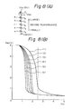
- Figure 8(A) shows a further NAND gate circuit embodying the invention having five input terminals provided with five driving transistors.
- the transistors T2 and T6 each have a V th of 0.6 V, a thickness of a gate oxide film of 350 ⁇ , a gate width of 50 ⁇ m, and a gate length of 2 ⁇ m, while the transistor T1 has a V th of -3.5 V, a thickness of a gate oxide film of 350 ⁇ , a gate width of 8 ⁇ m, and a gate length of 5 ⁇ m.
- Figure 8(B) is a graph of the input-output curve of the conventional NAND gate circuit.
- the curves (1) to (6) are obtained when the NAND gate circuit is operated at a V cc of 5 V.
- the lowest input threshold voltage of the NAND gate circuit is 1.40 V, obtained when only the input e was only varied, while the highest thereof is 2.40 V, obtained when all of these inputs a to e were changed.
- Figure 8(C) shows the input-output curves of the NAND gate circuit of Fig. 8(A).
- the five transistors T2 to T6 are divided into two groups, one composed of two transistors T2 and T3 and the other of three transistors T4 , T5 , and T6.
- Each transistor belonging to the former group has a V th of 0.6 V, while each of the latter group has a V th of 0.8 V.
- the lowest input threshold voltage of the NAND gate circuit is 1.65 V, obtained when only the input e was varied, while the highest input threshold voltage was 2.45 V, obtained when all of the inputs a to e were simultaneously varied.
- the noise immunity of the NAND gate circuit of Fig. 8(A) can be greater than the above-discussed conventional 5-input NAND gate cirucit.
- a NAND gate circuit embodying the present invention can provide improved overall noise immunity since the input threshold voltages of the NAND gate circuit obtained for all combinations of the input signals can be set at nearly the same value.
- Such a NAND gate circuit is less prone to operate erroneously under noisy input conditions, so erroneous operation of a memory cell array connected to the NAND gate in a semiconductor memory, for example, caused by noise can also effectively be prevented.
Landscapes
- Engineering & Computer Science (AREA)
- Physics & Mathematics (AREA)
- Computer Hardware Design (AREA)
- Computing Systems (AREA)
- General Engineering & Computer Science (AREA)
- Mathematical Physics (AREA)
- Power Engineering (AREA)
- Read Only Memory (AREA)
- Dram (AREA)
- Electronic Switches (AREA)
- Logic Circuits (AREA)
Applications Claiming Priority (2)
| Application Number | Priority Date | Filing Date | Title |
|---|---|---|---|
| JP63269408A JP2555165B2 (ja) | 1988-10-27 | 1988-10-27 | ナンド回路 |
| JP269408/88 | 1988-10-27 |
Publications (3)
| Publication Number | Publication Date |
|---|---|
| EP0366489A2 true EP0366489A2 (de) | 1990-05-02 |
| EP0366489A3 EP0366489A3 (en) | 1990-08-16 |
| EP0366489B1 EP0366489B1 (de) | 1995-07-05 |
Family
ID=17471999
Family Applications (1)
| Application Number | Title | Priority Date | Filing Date |
|---|---|---|---|
| EP89311123A Expired - Lifetime EP0366489B1 (de) | 1988-10-27 | 1989-10-27 | NAND Gateschaltungen |
Country Status (5)
| Country | Link |
|---|---|
| US (1) | US5059825A (de) |
| EP (1) | EP0366489B1 (de) |
| JP (1) | JP2555165B2 (de) |
| KR (1) | KR930005652B1 (de) |
| DE (1) | DE68923343T2 (de) |
Families Citing this family (4)
| Publication number | Priority date | Publication date | Assignee | Title |
|---|---|---|---|---|
| JP2928651B2 (ja) * | 1991-03-19 | 1999-08-03 | 株式会社日立製作所 | 通信機能を備えた制御装置 |
| US5146115A (en) * | 1991-07-26 | 1992-09-08 | Zilog, Inc. | Domino-logic decoder |
| US5391941A (en) * | 1993-09-23 | 1995-02-21 | Cypress Semiconductor Corporation | Decoder circuitry with balanced propagation delay and minimized input capacitance |
| US7821866B1 (en) | 2007-11-14 | 2010-10-26 | Cypress Semiconductor Corporation | Low impedance column multiplexer circuit and method |
Family Cites Families (10)
| Publication number | Priority date | Publication date | Assignee | Title |
|---|---|---|---|---|
| JPS5315055A (en) * | 1976-07-27 | 1978-02-10 | Toshiba Corp | Logic circuit |
| US4250406A (en) * | 1978-12-21 | 1981-02-10 | Motorola, Inc. | Single clock CMOS logic circuit with selected threshold voltages |
| JPS5767333A (en) * | 1980-10-15 | 1982-04-23 | Matsushita Electric Ind Co Ltd | Mos integrated circuit |
| JPS5979487A (ja) * | 1982-10-27 | 1984-05-08 | Nec Corp | デコ−ダ回路 |
| US4649296A (en) * | 1984-07-13 | 1987-03-10 | At&T Bell Laboratories | Synthetic CMOS static logic gates |
| JPS61265794A (ja) * | 1985-05-20 | 1986-11-25 | Fujitsu Ltd | 半導体記憶装置のデコ−ダ回路 |
| FR2596595B1 (fr) * | 1986-03-28 | 1988-05-13 | Radiotechnique Compelec | Porte logique mos du type domino |
| JPS63228494A (ja) * | 1987-03-18 | 1988-09-22 | Fujitsu Ltd | ダイナミツク型デコ−ダ回路 |
| US4797580A (en) * | 1987-10-29 | 1989-01-10 | Northern Telecom Limited | Current-mirror-biased pre-charged logic circuit |
| US4851716A (en) * | 1988-06-09 | 1989-07-25 | National Semiconductor Corporation | Single plane dynamic decoder |
-
1988
- 1988-10-27 JP JP63269408A patent/JP2555165B2/ja not_active Expired - Lifetime
-
1989
- 1989-10-19 US US07/424,038 patent/US5059825A/en not_active Expired - Lifetime
- 1989-10-27 KR KR1019890015523A patent/KR930005652B1/ko not_active Expired - Lifetime
- 1989-10-27 EP EP89311123A patent/EP0366489B1/de not_active Expired - Lifetime
- 1989-10-27 DE DE68923343T patent/DE68923343T2/de not_active Expired - Fee Related
Also Published As
| Publication number | Publication date |
|---|---|
| JPH02117212A (ja) | 1990-05-01 |
| DE68923343D1 (de) | 1995-08-10 |
| JP2555165B2 (ja) | 1996-11-20 |
| US5059825A (en) | 1991-10-22 |
| US5059825B1 (de) | 1992-11-10 |
| EP0366489B1 (de) | 1995-07-05 |
| EP0366489A3 (en) | 1990-08-16 |
| KR900007188A (ko) | 1990-05-09 |
| DE68923343T2 (de) | 1995-11-23 |
| KR930005652B1 (ko) | 1993-06-23 |
Similar Documents
| Publication | Publication Date | Title |
|---|---|---|
| US4523301A (en) | Associative memory | |
| US5018107A (en) | Semiconductor memory device | |
| EP0408037A2 (de) | Halbleiterspeicheranordnung | |
| US4813022A (en) | Static memory with pull-up circuit for pulling-up a potential on a bit line | |
| KR950001126B1 (ko) | 메모리 회로 | |
| US4873673A (en) | Driver circuit having a current mirror circuit | |
| US4985646A (en) | Output buffer circuit of semiconductor integrated circuit | |
| US4937480A (en) | BICMOS buffer circuit | |
| US4833646A (en) | Programmable logic device with limited sense currents and noise reduction | |
| US4769564A (en) | Sense amplifier | |
| KR100266901B1 (ko) | 내부 전원 전압 발생 회로 및 그것을 이용한 반도체 메모리 장치 | |
| EP0366489B1 (de) | NAND Gateschaltungen | |
| US6154065A (en) | Sense amplifier circuit | |
| JP3805802B2 (ja) | 半導体メモリ装置のデータ出力回路 | |
| US5075891A (en) | Memory with a variable impedance bit line load circuit | |
| KR100291153B1 (ko) | 스태틱램 | |
| US4709352A (en) | MOS read-only memory systems | |
| US5671181A (en) | Data read circuit used in semiconductor storage device | |
| US6456559B1 (en) | Semiconductor integrated circuit | |
| US5808934A (en) | Integrated logic circuit and EEPROM | |
| US6011739A (en) | Semiconductor memory | |
| EP0393027B1 (de) | Leseverstärker | |
| EP0188956A2 (de) | Datenwahlschaltung für CMOS-Festwertspeicher | |
| JPS6299981A (ja) | スタテイツクram | |
| US5617370A (en) | Semiconductor memory device with controllable charging characteristics of column lines |
Legal Events
| Date | Code | Title | Description |
|---|---|---|---|
| PUAI | Public reference made under article 153(3) epc to a published international application that has entered the european phase |
Free format text: ORIGINAL CODE: 0009012 |
|
| AK | Designated contracting states |
Kind code of ref document: A2 Designated state(s): DE FR GB |
|
| PUAL | Search report despatched |
Free format text: ORIGINAL CODE: 0009013 |
|
| AK | Designated contracting states |
Kind code of ref document: A3 Designated state(s): DE FR GB |
|
| 17P | Request for examination filed |
Effective date: 19901024 |
|
| 17Q | First examination report despatched |
Effective date: 19921211 |
|
| GRAA | (expected) grant |
Free format text: ORIGINAL CODE: 0009210 |
|
| AK | Designated contracting states |
Kind code of ref document: B1 Designated state(s): DE FR GB |
|
| REF | Corresponds to: |
Ref document number: 68923343 Country of ref document: DE Date of ref document: 19950810 |
|
| ET | Fr: translation filed | ||
| PLBE | No opposition filed within time limit |
Free format text: ORIGINAL CODE: 0009261 |
|
| STAA | Information on the status of an ep patent application or granted ep patent |
Free format text: STATUS: NO OPPOSITION FILED WITHIN TIME LIMIT |
|
| 26N | No opposition filed | ||
| REG | Reference to a national code |
Ref country code: GB Ref legal event code: IF02 |
|
| PGFP | Annual fee paid to national office [announced via postgrant information from national office to epo] |
Ref country code: FR Payment date: 20041008 Year of fee payment: 16 |
|
| PGFP | Annual fee paid to national office [announced via postgrant information from national office to epo] |
Ref country code: DE Payment date: 20041021 Year of fee payment: 16 |
|
| PGFP | Annual fee paid to national office [announced via postgrant information from national office to epo] |
Ref country code: GB Payment date: 20041027 Year of fee payment: 16 |
|
| PG25 | Lapsed in a contracting state [announced via postgrant information from national office to epo] |
Ref country code: GB Free format text: LAPSE BECAUSE OF NON-PAYMENT OF DUE FEES Effective date: 20051027 |
|
| PG25 | Lapsed in a contracting state [announced via postgrant information from national office to epo] |
Ref country code: DE Free format text: LAPSE BECAUSE OF NON-PAYMENT OF DUE FEES Effective date: 20060503 |
|
| GBPC | Gb: european patent ceased through non-payment of renewal fee |
Effective date: 20051027 |
|
| PG25 | Lapsed in a contracting state [announced via postgrant information from national office to epo] |
Ref country code: FR Free format text: LAPSE BECAUSE OF NON-PAYMENT OF DUE FEES Effective date: 20060630 |
|
| REG | Reference to a national code |
Ref country code: FR Ref legal event code: ST Effective date: 20060630 |