EP0367030A2 - Verfahren zur Herstellung dünner Schichten metastabiler binärer Verbindungen - Google Patents
Verfahren zur Herstellung dünner Schichten metastabiler binärer Verbindungen Download PDFInfo
- Publication number
- EP0367030A2 EP0367030A2 EP89119379A EP89119379A EP0367030A2 EP 0367030 A2 EP0367030 A2 EP 0367030A2 EP 89119379 A EP89119379 A EP 89119379A EP 89119379 A EP89119379 A EP 89119379A EP 0367030 A2 EP0367030 A2 EP 0367030A2
- Authority
- EP
- European Patent Office
- Prior art keywords
- substrate
- film
- latent
- rapid thermal
- chromium
- Prior art date
- Legal status (The legal status is an assumption and is not a legal conclusion. Google has not performed a legal analysis and makes no representation as to the accuracy of the status listed.)
- Granted
Links
Images



Classifications
-
- G—PHYSICS
- G11—INFORMATION STORAGE
- G11B—INFORMATION STORAGE BASED ON RELATIVE MOVEMENT BETWEEN RECORD CARRIER AND TRANSDUCER
- G11B5/00—Recording by magnetisation or demagnetisation of a record carrier; Reproducing by magnetic means; Record carriers therefor
- G11B5/84—Processes or apparatus specially adapted for manufacturing record carriers
-
- G—PHYSICS
- G11—INFORMATION STORAGE
- G11B—INFORMATION STORAGE BASED ON RELATIVE MOVEMENT BETWEEN RECORD CARRIER AND TRANSDUCER
- G11B5/00—Recording by magnetisation or demagnetisation of a record carrier; Reproducing by magnetic means; Record carriers therefor
- G11B5/84—Processes or apparatus specially adapted for manufacturing record carriers
- G11B5/85—Coating a support with a magnetic layer by vapour deposition
Definitions
- the present invention relates to the field of high density recording systems suitable for computer data storage. More particularly, it relates to a new thin-film CrO2 recording medium and to a method for producing same.
- Chromium dioxide (CrO2) is well known for its use as a recording medium in high grade magnetic recording tapes. It is used in particulate form. This particulate form of the material prevents its application to high density (gigabit) storage. It has not been possible previously to make acceptable smooth, continuous thin films of CrO2. This results from the metastable nature of CrO2 at room temperature. The only previously known method of depositing thin films of CrO2 have been by chemical transport methods ("Epitaxial Growth of CrO2 on sapphire in air", Japan J. Appl. Phys., Vol. 17, (1978), 249.). This transport method used flowing O2 at atmospheric pressure and high temperatures. The substrates are also heated.
- CrO2 is also a useful recording material for optical recording ("CrO2 predicted as a half-metallic ferromagnet", K. Schwarz, J. Phys. F. Met. Phys . Vol. 16 (1986) 0p. 211-215.).
- the Faraday rotation is -5.2X10⁴deg/cm for light of 2.5 eV photon energy.
- Rapid thermal annealing is a known method step in semiconductor device processing which has been in use over the past few years. This method has been used in silicon device technology to:
- the sample is brought up to a very high temperature (700 - 1000°C) in very short time (order of few milliseconds and shorter).
- a very high temperature 700 - 1000°C
- very short time order of few milliseconds and shorter.
- the energetic particle bombardment mechanism used to form the latent film forming CrO x mixture includes RF sputtering, magnetron sputtering, diode sputtering, ion plating, ion beam sputtering or arc evaporation of the metallic chromium in an O2 atmosphere wherein chromium ions provide the energetic particle bombardment which produces active nuclei on the substrate in the latent mixture.
- the objects of the present invention are accomplished by a process for forming thin films of chromium dioxide on a suitable substrate, which film is receptive to high density magnetic recording.
- the process comprises depositing both chromium and oxygen atoms on the substrate by evaporative techniques in an evacuated chamber and concurrently bombarding the substrate with high energy ions of at least one of the film constituents to form a latent CrO x film forming layer.
- the steps are carried out at approximately room temperature.
- the process is enhanced if the substrate is maintained at a temperature of between 10 and 40°C.
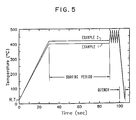
- the as-grown latent film forming layer is subsequently treated by a rapid thermal anneal step which raises the temperature of the as-grown film to about 500°C within a time period of about 10 seconds after preheating the film to about 400°C for about 90 seconds.
- the rapid thermal anneal step preferably comprises a series of at least five separate pulses over said 10-second time span. After the rapid thermal anneal the sample is rapidly quenched to room temperature.
- the present invention consists of a novel CrO2 thin film structure and a process for making that structure. A plurality of steps are involved in the process. These are generally described below. First the structure (device) will be described, then the processing steps, and then some more structural and process considerations will be presented.
- the structure is a CrO2 thin film recording medium containing suitable anisotropic dopants with a thickness that is acceptable for the required magnetic recording bit density.
- This film is deposited onto a suitable substrate.
- a substrate such as an aluminum alloy disc or a silicon wafer is used.
- the recording medium is then protected with a Cr2O3 film whose thickness is consistent with read-write head and recording medium separation.
- the thickness of typical films would be 100 nm for the CrO2 thickness and 15 nm for the Cr2O3.
- anisotropic dopant materials such as Fe, Co, Sb, In, etc. (or their compounds) may be added to the CrO2.
- the process for depositing one or both of the films involves simultaneous vapor deposition of chromium and ion bombardment of the growing film with energetic oxygen particle ions, atoms or molecules.
- the relative metal atom, ion, and neutral background molecule fluxes and ion energies are determined by material requirements known to those skilled in the art.
- Both the CrO2 and Cr2O3 films (if the latter is desired as an insulation or protective layer) can be deposited in one evaporation process cycle. The transition from one compound to the other, which is determined by the relative fluxes and energies of the particles arriving at the growing film surfaces, will be described subsequently.
- the ion bombardment concurrent with film deposition produces an initial latent CrO x film mixture having active centers/sites that direct the path for nucleating the metastable nonequilibrium phase CrO2.
- This reaction path requires that the chromium atom to oxygen ratio be in a range close to the CrO2 composition, that the active centers/sites be induced by energetic particle bombardment (preferably oxygen), and that the thermal anneal be rapid and highly nonequilibrium.
- the as-deposited or latent mixture films are amorphous and have poor magnetic properties.
- the magnetic properties of the amorphous CrO2 are improved by nonequilibrium heating (e.g., rapid thermal annealing).
- This rapid thermal processing to the knowledge of the inventors, has never been applied to nucleate or grow particular chromium oxide binary compound films. It has been used in silicon processing.
- the nonequilibrium nature of the annealing is used to prevent the non-ferromagnetic Cr2O3 (the lowest energy phase) from growing. If the films have not been bombarded with ions during growth, the ferromagnetic CrO2 state will not grow using this process. Accordingly, the ion bombardment, of one type or another, is a critical process parameter.
- the CrO2 is deposited by vapor depositing the Cr at a rate corresponding to 1.0-1.2 nm/sec while simultaneously bombarding the film with O2+ ions with an energy of 200-600 eV and beam current density of 0.5-2.5mA/cm2 with the substrate held at between 10-40°C. These depositions should be done with an O2 background pressure of between 6.67x10 ⁇ 3 and 10.66x10 ⁇ 3 Pa (5X10 ⁇ 5 and 3X10 ⁇ 5 Torr).
- Cr2O3 may be deposited as part of the same overall process using procedures similar to the CrO2 except that the deposition parameters are somewhat different.
- This insulating Cr2O3 material is deposited with substrate temperatures between 40°-80°C using lower energy O2+ ions or mixtures of Ar+ and O2+ ions.
- O2+ ion energies 200-600 eV and beam current densities of 0.5-2.5 mA/cm2 in an O2+ background pressure of 10.66x10 ⁇ 3 Pa (8.X10 ⁇ 5 Torr) are required.
- mixtures of Ar and O2 are used in the ion source, e.g., 50% of each, Cr2O3 films are always obtained.
- Fig 1 shows a simplified apparatus suitable for practicing the present invention.
- a chromium source 10 is placed on a suitable surface 12 for heating (not shown).
- Oxygen is introduced through a suitable ionization device 14 from which it is directed onto a sample substrate 16.
- Substrate heating and temperature control is also provided.
- the process is carried out in a suitable containment chamber 18 which is evacuated by connection to a vacuum pump. Suitable energies are imparted to the Cr atoms and O2 ions by biasing the various elements within the ranges taught herein.
- the magnetic properties of the amorphous CrO2 are improved by substrate heating.
- oxides of chromium can be readily grown by this method.
- Thin films of CrO x (where x varies from 1.6 to 3) have been obtained by evaporation with simultaneous ion bombardment in an oxygen background pressure of 5.33x10 ⁇ 3 to 2.67x10 ⁇ 2 Pa (4x10 ⁇ 6 to 2x10 ⁇ 4 Torr).
- the films obtained were 1500 ⁇ thick.
- Silicon substrates and insulating substrates such as quartz, sapphire, amorphous SiO2 on silicon, etc. were used. By X-ray diffraction the films were amorphous.
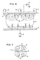
- These films were subjected to rapid thermal annealing in a setup heated with four 1kW flash lamps 70 (as shown in Fig. 7). The peak temperature was controlled by an automatic power controller (not shown).
- the samples 76 were placed on a quartz platform 74.
- the whole annealing step is carried out in a suitable container in an air or oxygen atmosphere.
- Reflectors 78 perform the function of concentrating the energy produced by the flash lamps 70 into the samples 76.
- Other rapid thermal processes such as electron bombardment, as is well known in the art, laser flash annealing or other energetic proton beam processes such as microwaves.
- a time versus temperature profile is shown in Fig. 5. Soak temperatures of 400, and 430°C were used. These were reached with a very steep temperature-time ramp. The samples reached the desired temperature (as measured by a thermocouple placed near the sample) within 40 seconds. At this temperature, the samples were soaked (kept at the elevated temperature) for periods of time ranging from 30 seconds to 2 minutes. After this soak period, the specimens were given uniformly 5 flashes over 10 seconds. The peak temperatures reached were 490°C. As soon as the peak was reached the controller was switched off and the samples quenched.
- heat sources other than radiant energy can be used for the rapid thermal annealing.
- radiant energy e.g., flash tube
- electron beams can be used.
- In situ observations of electron beam rapid thermal annealing into the CrO2 phase have been made in a Transmission Electron Microscope (TEM).
- TEM Transmission Electron Microscope
- anisotropy directions can be controlled. For example, ion bombardment with an ion velocity component parallel to the film surface has been used to create an anisotropy direction in the plane of the film.
- Fig. 6 is a schematic cross-section of a magnetron sputtering set-up in which energetic Cr ions impinge on the sample substrates 60.
- a chromium cathode 61 is connected to a suitable dc or rf supply 62 with a matching network, as in the lower sample support 63.
- the magnetron produces a magnetic field 64 via pole pieces 65. This field in turn produces intense glow regions 66 and the less intense glow region 67.
- Energetic chromium ions (Cr) are shown moving toward the sample substrates 60.
- the O2+ ions are also shown.
- the Ar+ ions are shown also.
Landscapes
- Manufacturing Of Magnetic Record Carriers (AREA)
- Physical Vapour Deposition (AREA)
- Thin Magnetic Films (AREA)
Applications Claiming Priority (2)
| Application Number | Priority Date | Filing Date | Title |
|---|---|---|---|
| US07/263,839 US4925700A (en) | 1988-10-28 | 1988-10-28 | Process for fabricating high density disc storage device |
| US263839 | 1988-10-28 |
Publications (3)
| Publication Number | Publication Date |
|---|---|
| EP0367030A2 true EP0367030A2 (de) | 1990-05-09 |
| EP0367030A3 EP0367030A3 (de) | 1991-05-02 |
| EP0367030B1 EP0367030B1 (de) | 1996-01-17 |
Family
ID=23003448
Family Applications (1)
| Application Number | Title | Priority Date | Filing Date |
|---|---|---|---|
| EP89119379A Expired - Lifetime EP0367030B1 (de) | 1988-10-28 | 1989-10-19 | Verfahren zur Herstellung dünner Schichten metastabiler binärer Verbindungen |
Country Status (4)
| Country | Link |
|---|---|
| US (1) | US4925700A (de) |
| EP (1) | EP0367030B1 (de) |
| JP (1) | JPH0765158B2 (de) |
| DE (1) | DE68925459T2 (de) |
Families Citing this family (9)
| Publication number | Priority date | Publication date | Assignee | Title |
|---|---|---|---|---|
| US4980198A (en) * | 1989-11-30 | 1990-12-25 | Syracuse University | Laser CVD and plasma CVD of CrO2 films and cobalt doped CrO2 films using organometallic precursors |
| JPH03242983A (ja) * | 1990-02-06 | 1991-10-29 | Internatl Business Mach Corp <Ibm> | 磁気構造体の製造方法 |
| US5480534A (en) * | 1990-08-22 | 1996-01-02 | Toa Electronics Ltd. | Electrode for measuring PH |
| AU5483196A (en) * | 1995-04-14 | 1996-10-30 | Spectra-Physics Lasers, Inc. | Method for producing dielectric coatings |
| FR2753567B1 (fr) * | 1996-09-19 | 1998-11-13 | Alsthom Cge Alcatel | Procede de depot d'un film ferromagnetique sur un guide d'onde, et un composant magneto-optique comprenant un film mince ferromagnetique depose selon le procede |
| RU2104592C1 (ru) * | 1997-02-21 | 1998-02-10 | Йелстаун Корпорейшн Н.В. | Способ изготовления магнитного носителя |
| JP4521644B2 (ja) * | 1999-04-13 | 2010-08-11 | シャープ株式会社 | 光触媒膜の形成方法 |
| US9932664B2 (en) * | 2012-11-06 | 2018-04-03 | Purdue Research Foundation | Methods for directed irradiation synthesis with ion and thermal beams |
| WO2015112358A1 (en) * | 2014-01-24 | 2015-07-30 | Tokyo Electron Limited | Method and system for performing post-etch annealing of a workpiece |
Family Cites Families (2)
| Publication number | Priority date | Publication date | Assignee | Title |
|---|---|---|---|---|
| JPS5935436B2 (ja) * | 1978-11-02 | 1984-08-28 | フオ−ド モ−タ− カンパニ− | 真空蒸着方法 |
| JPS6115967A (ja) * | 1984-06-29 | 1986-01-24 | Sumitomo Electric Ind Ltd | 表面処理方法 |
-
1988
- 1988-10-28 US US07/263,839 patent/US4925700A/en not_active Expired - Fee Related
-
1989
- 1989-09-20 JP JP1242399A patent/JPH0765158B2/ja not_active Expired - Lifetime
- 1989-10-19 DE DE68925459T patent/DE68925459T2/de not_active Expired - Fee Related
- 1989-10-19 EP EP89119379A patent/EP0367030B1/de not_active Expired - Lifetime
Also Published As
| Publication number | Publication date |
|---|---|
| DE68925459T2 (de) | 1996-09-05 |
| JPH0765158B2 (ja) | 1995-07-12 |
| EP0367030A3 (de) | 1991-05-02 |
| US4925700A (en) | 1990-05-15 |
| EP0367030B1 (de) | 1996-01-17 |
| JPH02129361A (ja) | 1990-05-17 |
| DE68925459D1 (de) | 1996-02-29 |
Similar Documents
| Publication | Publication Date | Title |
|---|---|---|
| Yu et al. | Control of thin film orientation by glancing angle ion bombardment during growth | |
| Sonnenberg et al. | Preparation of biaxially aligned cubic zirconia films on pyrex glass substrates using ion‐beam assisted deposition | |
| Rossnagel et al. | Film modification by low energy ion bombardment during deposition | |
| Oura et al. | LEED-AES study of the Au Si (100) system | |
| Dworschak et al. | Growth mechanism of cubic boron nitride in a rf glow discharge | |
| US5603766A (en) | Method for producing uniaxial tetragonal thin films of ternary intermetallic compounds | |
| US4125446A (en) | Controlled reflectance of sputtered aluminum layers | |
| EP0367030B1 (de) | Verfahren zur Herstellung dünner Schichten metastabiler binärer Verbindungen | |
| JP2003158307A (ja) | 超伝導材料の製造方法 | |
| Canali et al. | Solid‐phase epitaxial growth of Si through palladium silicide layers | |
| Barth et al. | Influence of the deposition parameters on boron nitride growth mechanisms in a hollow cathode arc evaporation device | |
| Park et al. | Growth mechanism of cubic boron nitride thin films by ion beam assist sputter deposition | |
| Zhang et al. | Structure and thermal stability of copper nitride thin films | |
| Lo et al. | Magnetic and structural properties of high rate dual ion‐beam sputtered NiFe films | |
| JPH0280562A (ja) | 鉄ガーネット層の製造方法、光導波路およびインテグレーテッドオプトエレクトロニクス素子 | |
| US5876790A (en) | Vacuum evaporation method for producing textured C60 films | |
| EP0486054B1 (de) | Verfahren zur Herstellung einer supraleitenden Oxyd-Dünnschicht | |
| US5863661A (en) | Method of enhancing the c-axis perpendicular orientation of barium hexaferrite thin films and barium hexaferrite thin film recording media produced thereby | |
| Lee | Grain size control of Bi-substituted garnet films crystallized by multi-step rapid thermal annealing for magneto-optical disks | |
| Shinohara et al. | ICB deposition and epitaxial growth of GaAs thin films | |
| JP2985472B2 (ja) | シリコン膜の形成方法 | |
| Dijkkamp et al. | Rapid laser‐induced growth of nitride and oxide layers at a beryllium/liquid interface | |
| RU2122243C1 (ru) | Способ получения магнитомягких термостойких аморфных конденсатов 3d-металлов | |
| Bernstein et al. | Magnetron sputtering of Fe onto GaAs substrates: Energetic bombardment effects | |
| US4001481A (en) | Superconductive elements and method for producing the same |
Legal Events
| Date | Code | Title | Description |
|---|---|---|---|
| PUAI | Public reference made under article 153(3) epc to a published international application that has entered the european phase |
Free format text: ORIGINAL CODE: 0009012 |
|
| AK | Designated contracting states |
Kind code of ref document: A2 Designated state(s): DE FR GB |
|
| 17P | Request for examination filed |
Effective date: 19900820 |
|
| PUAL | Search report despatched |
Free format text: ORIGINAL CODE: 0009013 |
|
| AK | Designated contracting states |
Kind code of ref document: A3 Designated state(s): DE FR GB |
|
| 17Q | First examination report despatched |
Effective date: 19930421 |
|
| GRAA | (expected) grant |
Free format text: ORIGINAL CODE: 0009210 |
|
| AK | Designated contracting states |
Kind code of ref document: B1 Designated state(s): DE FR GB |
|
| REF | Corresponds to: |
Ref document number: 68925459 Country of ref document: DE Date of ref document: 19960229 |
|
| ET | Fr: translation filed | ||
| PG25 | Lapsed in a contracting state [announced via postgrant information from national office to epo] |
Ref country code: GB Effective date: 19961019 |
|
| PLBE | No opposition filed within time limit |
Free format text: ORIGINAL CODE: 0009261 |
|
| STAA | Information on the status of an ep patent application or granted ep patent |
Free format text: STATUS: NO OPPOSITION FILED WITHIN TIME LIMIT |
|
| 26N | No opposition filed | ||
| GBPC | Gb: european patent ceased through non-payment of renewal fee |
Effective date: 19961019 |
|
| PG25 | Lapsed in a contracting state [announced via postgrant information from national office to epo] |
Ref country code: FR Effective date: 19970630 |
|
| PG25 | Lapsed in a contracting state [announced via postgrant information from national office to epo] |
Ref country code: DE Effective date: 19970701 |
|
| REG | Reference to a national code |
Ref country code: FR Ref legal event code: ST |