EP0367266A2 - Appareil à reproduire une image numérique - Google Patents
Appareil à reproduire une image numérique Download PDFInfo
- Publication number
- EP0367266A2 EP0367266A2 EP89120306A EP89120306A EP0367266A2 EP 0367266 A2 EP0367266 A2 EP 0367266A2 EP 89120306 A EP89120306 A EP 89120306A EP 89120306 A EP89120306 A EP 89120306A EP 0367266 A2 EP0367266 A2 EP 0367266A2
- Authority
- EP
- European Patent Office
- Prior art keywords
- image
- light
- liquid crystal
- medium
- memory means
- Prior art date
- Legal status (The legal status is an assumption and is not a legal conclusion. Google has not performed a legal analysis and makes no representation as to the accuracy of the status listed.)
- Withdrawn
Links
Images

Classifications
-
- G—PHYSICS
- G06—COMPUTING OR CALCULATING; COUNTING
- G06T—IMAGE DATA PROCESSING OR GENERATION, IN GENERAL
- G06T1/00—General purpose image data processing
-
- G—PHYSICS
- G06—COMPUTING OR CALCULATING; COUNTING
- G06K—GRAPHICAL DATA READING; PRESENTATION OF DATA; RECORD CARRIERS; HANDLING RECORD CARRIERS
- G06K1/00—Methods or arrangements for marking the record carrier in digital fashion
- G06K1/12—Methods or arrangements for marking the record carrier in digital fashion otherwise than by punching
- G06K1/126—Methods or arrangements for marking the record carrier in digital fashion otherwise than by punching by photographic or thermographic registration
-
- G—PHYSICS
- G06—COMPUTING OR CALCULATING; COUNTING
- G06K—GRAPHICAL DATA READING; PRESENTATION OF DATA; RECORD CARRIERS; HANDLING RECORD CARRIERS
- G06K15/00—Arrangements for producing a permanent visual presentation of the output data, e.g. computer output printers
- G06K15/02—Arrangements for producing a permanent visual presentation of the output data, e.g. computer output printers using printers
- G06K15/12—Arrangements for producing a permanent visual presentation of the output data, e.g. computer output printers using printers by photographic printing, e.g. by laser printers
- G06K15/1238—Arrangements for producing a permanent visual presentation of the output data, e.g. computer output printers using printers by photographic printing, e.g. by laser printers simultaneously exposing more than one point
-
- G—PHYSICS
- G03—PHOTOGRAPHY; CINEMATOGRAPHY; ANALOGOUS TECHNIQUES USING WAVES OTHER THAN OPTICAL WAVES; ELECTROGRAPHY; HOLOGRAPHY
- G03B—APPARATUS OR ARRANGEMENTS FOR TAKING PHOTOGRAPHS OR FOR PROJECTING OR VIEWING THEM; APPARATUS OR ARRANGEMENTS EMPLOYING ANALOGOUS TECHNIQUES USING WAVES OTHER THAN OPTICAL WAVES; ACCESSORIES THEREFOR
- G03B2227/00—Photographic printing apparatus
- G03B2227/32—Projection printing apparatus, e.g. enlarging apparatus, copying camera
- G03B2227/325—Microcapsule copiers
Definitions
- the present invention relates to a digital image outputting apparatus for visualizing and outputting a digital image on a paper surface on the basis of the data thereof.
- Conventional digital image outputting apparatus comprise a first image medium, which can be exposed for a short time period of one millisecond or less but is difficult to have a large area, a second image medium, which is difficult to expose for the short time period, a laser scanner, which writes an image according to an image data in the first image medium, and a project medium, which project the image written in the first image medium on the second image medium.
- FIG. 2 One example of the digital image outputting apparatus is shown in Fig. 2.
- a photoconductive image medium 1 of Se or the like is supported by a guide bar 2 so that it can move along the guide bar 2.
- a laser write unit 3 is composed of a corona charger 3a, a laser scanner 3b and a toner developing device 3c.
- the luminous flux emanating from the laser scanner 3b is scanned at a high speed in the direction of arrow x.
- the laser write unit 3 as a whole is movable in the direction of arrow y perpendicular to the direction of the arrow x.
- the laser write unit visualizes the image such that the photoconductive image medium 1 being moved at a constant speed in the direction of the arrow y is given at first a electric potential by the corona charger 3a, then a selective electric potential distribution by the laser scanner 3b, and a toner according to the electric potential distribution by the toner developing device 3c.
- the photoconductive image medium 1 thus written with the image in the form of toner density distribution is moved over the guide bar 2 to another position.
- a luminous flux 5 emanating from a light source 4 is condensed by a condenser lens system 6 into a parallel or converged luminous flux to go into the photoconductive image medium 1.
- the luminous flux 5 is reflected by the photoconductive image medium 1 and is focused on a microcapsule paper 8 by a projection lens 7 so that the image written in the photoconductive image medium 1 is imaged on the microcapsule paper 8.
- the positions to be written with the three images have to be precisely registered.
- the position of the laser scanner in the y direction and a rotating angle of a polygon mirror used in the laser scanner have to be precisely detected.
- the positions of a writing laser spot have to be precisely aligned among the three images, and the same side of the polygon mirror has always to be used when the same line of the image is to be scanned.
- the scanning speeds in the x and y directions and the rotating speed of the polygon mirror have to be controlled with a technically high difficulty so that the production cost of the apparatus is increased.
- An object of the present invention is to provide the digital image outputting apparatus for forming a written image of high quality.
- Another object of the present invention is to provide the digital image outputting apparatus for writing an image of high resolution by a relatively simple structure.
- the digital image outputting apparatus of the present invention comprises the first image medium such as a liquid crystal device, the second image medium such as a microcapsule paper, an optical system which projects an image of the first image medium to the second image medium, an image writing device which writes a desired image in the first image medium and is arranged in a conjugate position with the first image medium to a projection lens arranged between the first image medium and the second image medium, and a light path switching medium.
- the first image medium such as a liquid crystal device
- the second image medium such as a microcapsule paper
- an optical system which projects an image of the first image medium to the second image medium
- an image writing device which writes a desired image in the first image medium and is arranged in a conjugate position with the first image medium to a projection lens arranged between the first image medium and the second image medium
- a light path switching medium a light path switching medium.
- the apparatus of the present invention outputs the image using an image writing step and an image projecting step.
- the image writing step is that the light emanating from the image writing device is inserted into the light path of the optical system by the light path switching medium and is projected on the first image medium through the projection lens. As a result, the desired image is written in the first image medium.
- the image projecting step is that the image written in the first image medium is projected on the second image medium by the optical system. As a result, the desired image is formed on the second image medium.
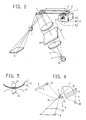
- Fig. 1 is a diagram showing the concept of an optical system of the embodiment of the present invention.
- An LED array head 10 is so supported that it moves in a plane containing its light emitting portion and in a direction generally vertical to the scanning direction of the light emitting portion.
- the moving plane of the light emitting portion of the LED array head 10 and a photoconductive liquid crystal panel 11 are positioned in conjugate relation to a projection lens 7 through a plane mirror 9.
- the transverse ratio of the photoconductive liquid crystal panel 11 to the plane containing the light emitting portion of the LED array head 10 is 1 or less.
- the photoconductive liquid crystal panel 11 is a combination of a liquid crystal panel and a photoconductive layer.
- the photoconductive layer is set to have sensitivity to the luminescent wavelength of the LED array head 10.
- the liquid crystal panel maintains the changed reflectivity after removing the bias electric field and a ray of light incident. These characteristics of the liquid crystal panel are called the memory properties.
- the photoconductive liquid crystal panel uses the liquid crystal panel which has the above-specified memory properties.
- the LED array head 10 is modulated according to image signals and is moved in its movable plane, and a desired image is written in the photoconductive liquid crystal panel 11 applied the bias electric field thereby.
- the plane mirror 9 is removed from an optical path which a luminous flux 5 passes.
- the luminous flux 5 emanating from the light source 4 is condensed by the condenser lens system 6 into the parallel or converged luminous flux, irradiates upon the photoconductive liquid crystal panel 11, is reflected by the photoconductive liquid crystal panel 11, and is focused on the microcapsule paper 8 by the projection lens 7.
- the image written on the photoconductive liquid crystal panel 11 is formed on the microcapsule paper 8.
- the photoconductive liquid crystal panel 11 is a medium for modulating the optical polarized state.
- Polarizers 21, 22 are arranged to convert the distribution of the polarized state into a light quantity distribution. At this time, it is of great advantage to a contrast of the image formed on the microcapsule paper 8 that the polarizers 21, 22 are set in the cross Nicol with the photoconductive liquid crystal panel 11 being unwritten.
- a catoptrics spherical mirror 24 is arranged at the back of the light source 4 and reflects the light emanating from the light source 4.
- Fig. 3 is a schematic diagram showing the developing portion of the microcapsule paper 8.
- the microcapsule paper 8 is that microcapsules 12, which have leuco-dyes and photosensitive resin, are evenly applied to a support film 13.
- the photosensitive resin of the microcapsules 12 harden in accordance with the quantities of light given so that the image written in the photoconductive liquid crystal panel 11 is formed with a latent image on the microcapsule paper 8.
- the microcapsule paper 8 is so superposed on a receiver paper 14 that its surface coated with the microcapsules 12 faces the receiver paper 14, and is pressed by a pressure device such as a pressure roller 15.
- a pressure device such as a pressure roller 15.
- Fig. 4 is a diagram showing the concept of an optical system for explaining the operations of writing an image in the photoconductive liquid crystal panel 11 and projecting the image to the microcapsule paper 8.
- Fig. 4 is a side view of the optical system of the embodiment of the image output device shown in Fig. 1.
- the plane mirror 9 rotates on a pivot 19 to take its position 9a, as indicated by broken line.
- the light emitting portion of the LED array head 10 is in a plane B vertical to the surface of the drawing so that the LED array is arranged vertically to the surface of the drawing.
- the luminous flux emanating from LED array head 10 is reflected by the plane mirror 9a and is condensed on the photoconductive liquid crystal panel 11 through the projection lens 7.
- the luminous pattern of the LED array head 10 is projected upon the photoconductive liquid crystal panel 11.
- the luminous pattern of the LED array head 10 is determined by the time-series write signal based upon the image data and is varied with the lapse of time.
- the LED array head 10 is moved at a constant speed synchronized with the write signal in the direction of arrow A of Fig. 4 so that a two-dimensional image is written in the photoconductive liquid crystal panel 11.
- the image is recorded as the distribution of the retardation of the liquid crystal on the photoconductive liquid crystal panel 11 but is not converted into a spatial optical strength pattern until the projected light passes through a polarizer and an analyzer upstream and downstream of it.
- the polarizer and the analyzer correspond to the polarizers 21, 22 shown in Fig. 4.
- a write position for writing the image especially, the position for obtaining a color image by repeating the writing and exposure several times is desired to provide reproducibility as well as possible.
- a primary scanning mechanism includes no mechanical part so that the writing timing can be determined wholly by the electric factors.
- the writing position can be adjusted with an excellent reproducibility either by detecting the position of the LED array head to start the image writing on the basis of the timing or by determining the write starting timing according to the timing at which the auxiliary scan is started.
- Fig. 8 is a flow chart for explaining the writing and auxiliary scanning flows. After the start of the auxiliary scanning, a driving pulse motor has its rotating speed gradually increased to accelerate the auxiliary scanning speed (at Step 101).
- This pulse motor accomplishes its accelerating drive a predetermined pulse number and takes its constant drive so that the auxiliary scanning speed takes a substantially constant speed (at Step 102). After this, the driving pulse number of the pulse motor reaches a predetermined number, or the auxiliary scanning position by the auxiliary scanning position detecting device comes to a predetermined position. If either of these is detected (at Step 103), the writing operation by the LED array head 10, i.e., the emission of the LED array head 10 is started (at Step 104) after a constant time from the detection signal. After the whole writing of one frame has been ended (at Step 105), the r.p.m.
- the present embodiment is freed from any factor for dislocating the writing position, if the writing operation is started when the auxiliary scanning position comes the predetermined position.
- the written image is projected on the microcapsule paper 8.
- the plane mirror 9 is moved to the position, as indicated by solid line, to open the optical path from the projection lens 7 to the microcapsule paper 8.
- the luminous flux 5 emanating from the light source 4 is converged by the condenser lens system 6, and goes through the polarizer 21 into the photoconductive liquid crystal panel 11.
- the luminous flux 5 is subjected to modulations relating to the spatial polarization component according to the recorded retardation distribution and goes as a spatial light quantity pattern into the microcapsule paper 8 through the projection lens 7 and the polarizer 22.
- Fig. 5 is a conceptional diagram for briefly describing the structure of the LED array head used here.
- a number of LED light emitting portions 32 are arranged in one or more rows over a support 31 and are connected with a driver 33 so that their light emissions are modulated on the basis of a write signal 35.
- a field lens 34 for condensing the luminous fluxes emanating from the light emitting portions 32 toward the projection lens 7.
- the field lens 34 is effective to focus efficiently the lights emanating from the individual light emitting portions 32 of the LED array upon the photoconductive liquid crystal panel 11. Without the field lens 34, the image has its uneven brightness made as a result of the shading.
- the extent of the shading can be lightened by controlling the light emission quantity of the LED without using the field lens 34. It is quite natural that the control of the light emission quantity and the field lens are used jointly.
- the image data have three data of three primary colors.
- the LED array head 10 is driven on the basis of a first data of three primary colors so that the image accordant to the first data is written in the photoconductive liquid crystal panel 11 applied the bias of the electric field. And using the light having the wavelength corresponding to the color of the first data, the image is projected to the microcapsule paper 8 through the projection lens 7 so that the image corresponding to the first data is formed on the microcapsule paper 8.
- the method of obtaining the light having the wavelength component corresponding to three primary colors is exemplified either by a method of selecting light sources in accordance with the individual wavelengths or by a method of switching a color filter 66 shown in Fig. 4 for the light source having a wide wavelength spectrum.
- the light source having the array-shaped or two-dimensional optical intensity distribution for writing the image can be exemplified by a liquid crystal shutter array, a CRT (Cathode Ray Tube), or a plasma light emitting array.
- a liquid crystal shutter array will be described with reference to the drawings.
- Fig. 6 is a diagram showing the concept of the structure of the liquid crystal shutter array.
- a linear light source 42 such as a fluorescent lamp or a halogen lamp
- these liquid crystal shutters 43 are connected with a driver 44 so that the transmissivities are modulated according to a write signal 46 based upon the image data.
- the luminous flux emanating from the linear light source 42 has its light quantity modulated according to the transmissivities of the liquid crystal shutters 43.
- a Fresnel field lens 45 is arranged in the vicinity of the liquid crystal shutter array and has absolutely the same operation as that of the field lens 34 having been described in connection with the LED array head.
- the Fresnel lens 45 may be replaced by an ordinary lens or used as the field lens of the LED array head.
- the number of lines of the aforementioned liquid crystal shutters 43 is so small that its light emitting pattern is one-dimensional, a two-dimensional image can be formed on the photoconductive liquid crystal panel 11 like the aforementioned case of the LED array head by accomplishing a scanning in the auxiliary direction.
- the two-dimensional image can also be formed on the photoconductive liquid crystal panel 11 by the auxiliary scanning with the CRT having a one-dimensional image pattern.
- a two-dimensional image can also be written without any auxiliary scanning, i.e., at one time by increasing the number of lines of the light emitting elements with the LED array, the liquid crystal shutter array, the CRT or plasma light emitting array.
- Fig. 7 is a section showing the concept of the structure of the photoconductive liquid crystal panel 11.
- a glass substrate 51 is formed with a transparent electrode 52 and further with a photoconductive layer 53 and a dielectric reflecting film 54.
- orientation layers 55 Across an SmC* liquid crystal layer 57, moreover, there are formed orientation layers 55.
- a transparent electrode 58 is formed and supported by a glass substrate 59.
- a spacer 56 which has functional to connect its upper and lower layers mechanically, to fix the thickness of the SmC* liquid crystal layer 57 and to confine the SmC* liquid crystal.
- a reflection reducing film 60 is usually formed at the incident side of the glass substrate 59.
- the photoconductive layer 53 is generally made of a function-separated type organic photoconductive film of a-Si, Se, Se-Te, or Cd-S.
- the incidence directions of the writing light and the projecting light are in the direction of arrow c of Fig. 7. If, at this time, the reflecting characteristics of the dielectric reflecting film 54 is set such that the reflectivity is high in the photosensitive wavelength range of the microcapsule paper whereas and the transmissivity is high in the wavelength range of near infrared rays corresponding to the writing light of the semiconductor laser, the writing and reading (or projecting )operations can be accomplished from the same side.
- the writing operations are thus accomplished with the electric field being applied in the direction opposite to the polarizing direction of the SmC* liquid crystal, the director of the written portion is reversed to change the retardation. Since the SmC* liquid crystal has the memory properties, the patterns once written will not disappear even after the writing light and the electric field are removed. As a result, the projection can be accomplished with an illumination light after the writing operation has been ended and the electric field has been removed.
- the movable plane mirror 9 is used but may be replaced by a half mirror which is fixed in the position 9a of the plane mirror 9, as indicated by the broken line. In this modification, there can be attained an advantage that the moving mechanism for the mirror need not be used.
- the photoconductive image medium should not be limited to the liquid crystal panel specified in the present embodiment but can be exemplified by a photoconductor such as Se, a-Si or OPC to be developed by the zerographic method or an electrooptical crystal such as BSO.
- the digital image outputting apparatus of the present invention can write an image of high resolution by a relatively simple structure without requiring a moving part of high speed operations such as a polygon mirror or a galvano mirror.
- the distortion in the image due to vibrations can be reduced, and the wiring timing in the primary scanning direction (i.e., in the direction of the light source array) and the writing timing in the auxiliary scanning direction (i.e., generally vertical to the primary scanning direction) can be accurately aligned to provide a color image having little color drift.
Landscapes
- Physics & Mathematics (AREA)
- Engineering & Computer Science (AREA)
- General Physics & Mathematics (AREA)
- Theoretical Computer Science (AREA)
- Optics & Photonics (AREA)
- General Engineering & Computer Science (AREA)
- Printers Or Recording Devices Using Electromagnetic And Radiation Means (AREA)
- Liquid Crystal (AREA)
- Optical Systems Of Projection Type Copiers (AREA)
- Photographic Developing Apparatuses (AREA)
- Dot-Matrix Printers And Others (AREA)
Applications Claiming Priority (2)
| Application Number | Priority Date | Filing Date | Title |
|---|---|---|---|
| JP278954/88 | 1988-11-04 | ||
| JP63278954A JPH02125767A (ja) | 1988-11-04 | 1988-11-04 | ディジタル画像出力装置 |
Publications (2)
| Publication Number | Publication Date |
|---|---|
| EP0367266A2 true EP0367266A2 (fr) | 1990-05-09 |
| EP0367266A3 EP0367266A3 (fr) | 1992-03-04 |
Family
ID=17604377
Family Applications (1)
| Application Number | Title | Priority Date | Filing Date |
|---|---|---|---|
| EP19890120306 Withdrawn EP0367266A3 (fr) | 1988-11-04 | 1989-11-02 | Appareil à reproduire une image numérique |
Country Status (3)
| Country | Link |
|---|---|
| EP (1) | EP0367266A3 (fr) |
| JP (1) | JPH02125767A (fr) |
| KR (1) | KR900008399A (fr) |
Cited By (1)
| Publication number | Priority date | Publication date | Assignee | Title |
|---|---|---|---|---|
| EP0961215A1 (fr) * | 1994-01-28 | 1999-12-01 | Kabushiki Kaisha Komatsu Seisakusho | Dispositif de commande pour dispositif de marquage |
Family Cites Families (4)
| Publication number | Priority date | Publication date | Assignee | Title |
|---|---|---|---|---|
| JPS5616149A (en) * | 1979-07-19 | 1981-02-16 | Fuji Xerox Co Ltd | Picture forming method |
| US4641156A (en) * | 1983-12-30 | 1987-02-03 | Casio Computer Co., Ltd. | Recording apparatus with double frequency driven liquid crystal shutter |
| US4699498A (en) * | 1985-09-06 | 1987-10-13 | Nec Corporation | Image projector with liquid crystal light shutter |
| US4701397A (en) * | 1986-02-26 | 1987-10-20 | The Mead Corporation | Method for forming images on plain paper and an imaging sheet useful therein |
-
1988
- 1988-11-04 JP JP63278954A patent/JPH02125767A/ja active Pending
-
1989
- 1989-11-02 EP EP19890120306 patent/EP0367266A3/fr not_active Withdrawn
- 1989-11-04 KR KR1019890015991A patent/KR900008399A/ko not_active Withdrawn
Cited By (1)
| Publication number | Priority date | Publication date | Assignee | Title |
|---|---|---|---|---|
| EP0961215A1 (fr) * | 1994-01-28 | 1999-12-01 | Kabushiki Kaisha Komatsu Seisakusho | Dispositif de commande pour dispositif de marquage |
Also Published As
| Publication number | Publication date |
|---|---|
| EP0367266A3 (fr) | 1992-03-04 |
| JPH02125767A (ja) | 1990-05-14 |
| KR900008399A (ko) | 1990-06-04 |
Similar Documents
| Publication | Publication Date | Title |
|---|---|---|
| US4122462A (en) | Image information recording apparatus | |
| US4336994A (en) | Multi-mode color copier | |
| EP0134472A2 (fr) | Appareil d'analyse à faisceau laser | |
| WO1982004352A1 (fr) | Appareil d'adressage optique de haute resolution | |
| JPH1065873A (ja) | 文書走査装置 | |
| US4980701A (en) | Non-impact printhead using a mask with a dye sensitive to and adjusted by light in a first spectrum to balance the transmission of light in a second spectrum emitted by an LED array | |
| JP3429304B2 (ja) | 画像形成装置及び2次元光走査装置 | |
| US4060322A (en) | Image information handling device | |
| CA1183258A (fr) | Systeme d'enregistrement | |
| GB1564864A (en) | Flying spot scanning system | |
| JP2002205426A (ja) | 選択可能な光源を備えた空間光変調器を使用する単色画像の印刷方法および装置 | |
| JPH05224142A (ja) | 光学出力装置におけるスポット位置制御のための電子光学制御装置とシステム | |
| EP0367266A2 (fr) | Appareil à reproduire une image numérique | |
| US5363128A (en) | Device and apparatus for scan line process direction control in a multicolor electrostatographic machine | |
| JP3432267B2 (ja) | カラープリントヘッド | |
| JPH05232392A (ja) | 電子光学制御装置を使用した光学出力装置におけるスポット位置制御方法 | |
| US6552741B2 (en) | Optical scanning device, image scanning method and photographic processing device | |
| EP0679036A2 (fr) | Dispositif de production d'images | |
| US5706075A (en) | Exposure apparatus for controlling the duration of exposure operations according to compensated exposure data | |
| JP2533809B2 (ja) | 画像処理装置 | |
| JPH1062704A (ja) | 光学走査装置 | |
| JPS5827123A (ja) | 多重ゲ−ト光バルブ | |
| US5325208A (en) | Image formation device for scanning an optical memory by intermittently irradiating a night beam in accordance with density of a pixel | |
| USRE38297E1 (en) | Internal drum scophony raster recording device | |
| JPH10333405A (ja) | 画像形成装置 |
Legal Events
| Date | Code | Title | Description |
|---|---|---|---|
| PUAI | Public reference made under article 153(3) epc to a published international application that has entered the european phase |
Free format text: ORIGINAL CODE: 0009012 |
|
| AK | Designated contracting states |
Kind code of ref document: A2 Designated state(s): DE FR GB |
|
| PUAL | Search report despatched |
Free format text: ORIGINAL CODE: 0009013 |
|
| AK | Designated contracting states |
Kind code of ref document: A3 Designated state(s): DE FR GB |
|
| STAA | Information on the status of an ep patent application or granted ep patent |
Free format text: STATUS: THE APPLICATION IS DEEMED TO BE WITHDRAWN |
|
| 18D | Application deemed to be withdrawn |
Effective date: 19911203 |