EP0367284A2 - Porte de sortie reconfigurable - Google Patents
Porte de sortie reconfigurable Download PDFInfo
- Publication number
- EP0367284A2 EP0367284A2 EP89120392A EP89120392A EP0367284A2 EP 0367284 A2 EP0367284 A2 EP 0367284A2 EP 89120392 A EP89120392 A EP 89120392A EP 89120392 A EP89120392 A EP 89120392A EP 0367284 A2 EP0367284 A2 EP 0367284A2
- Authority
- EP
- European Patent Office
- Prior art keywords
- data
- computer
- output
- port
- output devices
- Prior art date
- Legal status (The legal status is an assumption and is not a legal conclusion. Google has not performed a legal analysis and makes no representation as to the accuracy of the status listed.)
- Withdrawn
Links
Images


Classifications
-
- G—PHYSICS
- G06—COMPUTING OR CALCULATING; COUNTING
- G06F—ELECTRIC DIGITAL DATA PROCESSING
- G06F13/00—Interconnection of, or transfer of information or other signals between, memories, input/output devices or central processing units
- G06F13/38—Information transfer, e.g. on bus
- G06F13/382—Information transfer, e.g. on bus using universal interface adapter
- G06F13/385—Information transfer, e.g. on bus using universal interface adapter for adaptation of a particular data processing system to different peripheral devices
Definitions
- the present invention relates in general to an output port for a computer and in particular to a port that may be selectively configured by the computer to provide an interface between the computer and output devices requiring a variety of different interface arrangements for receiving data from and transmitting data to a computer.
- a computer typically communicates with an output device such as a printer through a port connected to the computer's bus.
- the port converts the data to a form suitable for transmission to the output device and forwards the converted data to the output device.
- the port may also convey status, alarm or other data from the output device to the computer, usually by storing the incoming data in a register, interrupting the computer, and allowing the computer to read access the register through the bus.
- Output devices require a wide variety of interface arrangements for communicating with a computer including various input/output data formats, external bus configurations and handshaking protocols.
- a port To provide an interface between any particular output device and a computer, a port must provide the appropriate logic to convert input data to a form expected by the output device or the computer, must have appropriate input/output terminals for the external busses of the computer and the output device and must include suitable internal logic to provide appropriate handshaking protocol for those busses.
- a manual or computer operable switch may selectively connect any one of the output devices to a single port.
- the computer when a computer drives several output devices requiring differing interface arrangements, the computer must employ a separate port for each output device. Multiple ports are expensive and occupy scarce space within a computer chassis.
- a reconfigurable port selectively provides an interface between a computer and any of several output devices requiring differing interface arrangements. Before communicating with any selected one of the output devices, the computer sends programming data configuring the port to provide the correct interface for the selected output device and to appropriately connect input and outputs terminals of the port to the selected device. The computer then communicates with the selected output device through the port.
- a programmable gate array within the port provides the necessary handshaking, data routing and conversion logic for the port.
- the programming data programs the gate array to operate in a manner appropriate for the selected output device.
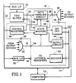
- a port 10 provides a computer 12 with selective access to any of several output devices (not shown).
- An output device such as for example a printer, receives input data or commands from the computer and may transmit status, alarm or other data to the computer in response to input commands.
- Output devices may require differing interface arrangements for transmitting and receiving data from a computer including for example, differing external bus configurations, differing input and output data formats, and differing handshaking protocols.
- computer 12 Before communicating with a selected one of the output devices, computer 12 sends programming data to port 10 via a bus 14.
- the programming data configures port 10 to provide the correct interface for the selected output device and appropriately connects input and output terminals of the port to input and output lines of the selected output device.
- computer 12 communicates with the selected output device through the port. Thereafter, before communicating with any other output device, the computer reconfigures the port to provide the correct interface for the other output device.
- a programmable gate array 16 within port 10 provides the necessary handshaking, data routing and data conversion logic for the port.
- Gate array 16 is illustrated in FIG. 1 as implementing the circuits shown within the dotted line.
- Gate array 16 suitably comprises a model XC2018 Logic Cell Array manufactured by XILINX, Inc. This device, described in detail in The Programmable Gate Array Design Handbook , published in 1986 by Xilinx, Inc., comprises an array of 100 configurable logic blocks and a set of 74 configurable I/O blocks. Each I/O block selectively provides an input or output interface between an external package pin and the logic block array.
- Each logic block has a combinatorial logic section, a storage element and a routing and control section.
- the combinatorial logic section produces an output which is a programmably selected Boolean function of up to four single bit inputs.
- the storage element in each logic block acts selectively as a flip-flop or a latch and may be employed to delay or store a data bit generated or received by the logic block.
- the internal routing and control section of each logic block adjustably interconnects the combinatorial logic section, the storage element and input and output terminals of the logic block.
- Programmably alterable routing circuitry within the gate array selectively connects input and output terminals of the various I/O and logic blocks to form a desired logic circuit.
- Computer 12 programs gate array 16 by transmitting to the gate array a sequence of programming data specifying I/O blocks to act as inputs and outputs, specifying the Boolean function performed by each logic block, specifying data routing paths within and between the logic blocks and specifying other configurable aspects of the gate array.
- Computer 12 supplies programming data and control signals to programming input terminals 18 of gate array 16 via a conventional bus interface circuit 20.
- port 10 includes an input multiplexer 22 connecting up to eight lines from a selected one of a plurality of output devices to input terminals 24 of gate array 16.
- An output multiplexer 26 connects up to eight output terminals 28 of gate array 16 to various lines of any selected one of the output devices.
- Port 10 also includes a first-in/first-out (FIFO) buffer 30 coupled to bus 14 through a conventional bus interface circuit 32.
- FIFO buffer 30 receives and stores sequences of data from computer 12.
- Output terminals of FIFO buffer 30 are connected to data input terminals 34 of gate array 16.
- FIFO buffer 30 When an output signal produced at an output terminal 36 of gate array 16 successively output enables FIFO buffer 30, FIFO buffer 30 successively forwards each element of its stored data data sequence to input terminals 34 of the gate array.
- computer 12 transmits configuration data to programming input terminals 18 of gate array 16 prior to communicating with a selected one of the output devices.
- the configuration data configures gate array 16 to act as a logic circuit performing various operations enabling computer 12 to communicate with the computer through bus 14 and to communicate with the selected output device through multiplexers 22 and 26.
- the configuration data also appropriately sets logic levels on various gate array 16 output terminals 40 and 42 connected to switching control inputs of multiplexers 22 and 26 so that these multiplexers connect output and input lines of the selected output device to input and output terminals 24 and 28 of logic array 16.
- a typical logic circuit implemented by gate array 16 includes a data handling circuit 38 connected between input terminals 34 and output terminals 28.
- Data handling circuit 38 receives data from computer 12 via FIFO buffer 30, converts the data to a form suitable for transmission to an external device, and then forwards the data to the selected external device via output multiplexer 26.
- a state machine 46 generates signals selecting and controlling various modes of circuit 38 operation.
- Computer 12 may also write commands or other data into an addressable control register 48 by placing the data on bus 14 along the address of the control register.
- a decoder 52 implemented by gate array 16 decodes the address and input enables the appropriate control register 48.
- the contents of one control register may provide an additional input to data handling circuit 38.
- data handling circuit 38 may forward the command stored in that control register 48 to an output device via output multiplexer 26.
- Data stored in one or more other control registers 48 controls operation of state machine 46.
- State machine 46 may transmit and receive handshaking signals when port 10 communicates with an output device. State machine 46 receives handshaking signals from an output device via input multiplexer 22, and transmits handshaking signals to the external device via output multiplexer 26. State machine 46 also generates the signal at output terminal 36 output enabling FIFO buffer 30, and may generate signals resetting or clearing various control registers 48 after reading their contents.
- An output circuit 50 receives and stores data transmitted from an output device via input multiplexer 22. In response to one or more output signals of state machine 46, interrupt circuit 54 transmits an interrupt signal (INT) to computer 12. Computer 12 responds to the interrupt signal by read accessing data stored in the interrupt circuit to determine the source of the interrupt and taking appropriate action, such as read accessing the data in output circuit 50.
- INT interrupt signal
- Port 10 may have several modes of operation depending on the interface arrangement of the output device the port is presently configured to service. For example, in a data transmission mode, computer 12 sends a sequence of data to FIFO buffer 30, and port 10 forwards the data in FIFO buffer 30 to a selected output device via output multiplexer 26. Computer 12 first sends the data sequence for storage in FIFO buffer 30 and then sends control data to state machine 46 via control registers 48 setting state machine 46 for the data transmission mode. State machine 46 thereafter sequentially output enables FIFO buffer 30 so that it sends each word of the sequence stored in the FIFO buffer to data handling circuit 38.
- State machine 46 provides the appropriate control input signals to data handling circuit 38 causing the data handling circuit to appropriately convert each data word read out of FIFO buffer 30 to a form suitable for transmission to the output device and to transmit the converted data words to the output device via output multiplexer 26. State machine 46 also monitors input handshaking signals from the output device via input multiplexer 22, and transmits the appropriate output handshaking signals to the output device via output multiplexer 26 to effect data transmission to the output device.
- Each data word of the data sequence stored in FIFO buffer 30 includes a bit indicating whether the data word is the last word of the sequence.
- the end of sequence indicating bit is provided as input to state machine 46.
- the process of forwarding data from the FIFO buffer to the output device continues until state machine 46 encounters the end of sequence indicating bit in FIFO buffer 30.
- state machine 46 signals interrupt circuit 54 to interrupt computer 12.
- Computer 12 then reads data in interrupt circuit 54 to determine the nature of the interrupt, and thereafter takes appropriate action, for example, sending another sequence to the FIFO buffer.
- Port 10 may also operate in a command mode whereby the computer 12 sends a command to an output device.
- a command may, for example, set the output device for a particular mode of operation or may tell the output device to return data indicating status of its internal settings or alarms.
- Computer 12 stores the command in one of control registers 48 and sets appropriate command mode indicating data in another control register 48.
- state machine 46 transmits control signals to data handling circuit 38 causing the data handling circuit to read the command out of a register 48, to convert the command to a form suitable to transmission to the output device, and to forward the converted command to the output device via output multiplexer 26.
- a command may tell an output device to return data indicating status of current internal settings or alarms of the output device.
- state machine 46 causes output circuit 50 to store the status data and then interrupts computer 12 via interrupt circuit 54.
- computer 12 reads data in interrupt circuit 54 indicating the nature of the interrupt, and then reads the status data stored in output circuit 50.
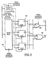
- FIG. 2 shows a suitable interrupt circuit 54 in more detailed block diagram form.
- Computer 12 of FIG. 1 writes a mask data word into a mask register 62 via bus 14. Each bit in mask register 62 controls a D input of a separate type D flip-flop 60.
- the computer may clear each flip-flop 60 by placing a clear bit on one line of bus 14 and latching the bit onto clear inputs of flip-flops 60 via a latch 64.
- Latch 64 and register 62 are selectively enabled by address decoder 52 of FIG. 1 in response to particular addresses placed on bus 14. Indicating signal outputs of state machine 46 of FIG. 1 separately clock flip-flops 60.
- the Q outputs of flip-flops 60 each drive a separate input of an OR gate 66 generating the interrupt signal (INT).
- a tristate buffer 68 latches the Q outputs of flip-flops 60 onto separate lines of bus 14 when enabled by a signal from address decoder 52 of FIG. 1 in response to a particular address on bus 14.
- Each bit of the mask data in mask register 62 may be set to a logical 1 when a corresponding control output bit of the state machine is to initiate an interrupt.
- the state machine asserts a control signal output, it clocks one of the flip-flops 60, and the flip-flop sets its Q output if its D input is driven by a logical "1" bit in mask register 62.
- the Q output drives the interrupt signal high through OR gate 66.
- the computer reads the output of tristate buffer 68, the particular bit of the buffer output that is a "1" tells the computer which signal output of the state machine initiated the interrupt. This enables the computer to determine the purpose of the interrupt and to take appropriate action.
- the computer may not want to service certain interrupts.
- the computer can prevent any particular control output signals of the state machine from initiating an interrupt by setting to a logical "0" the bit in mask register 62 controlling the D input of the flip-flop 60 clocked by the state machine output signal.
- FIG. 3 illustrates detailed configuration of port 10 when providing an interface between computer 12 and an example external device 70.
- Device 70 may be, for example, a printer including a state machine 72, a bi-directional, serial-parallel, parallel-serial shift register 74 and other circuits 76 for controlling printer operation in response to input data and for generating output data indicating printer status in response to a command from the computer.
- shift register 74 receives an 8-bit command (CMD) in serial form from port 10, converts the command to an 8-bit parallel data word, and forwards it to circuits 76.
- the command may, for example, tell circuits 76 to return an 8-bit status word (STAT) indicating current status of internal settings or alarms of the output device.
- shift register 74 stores an 8-bit parallel status word STAT from circuits 76 and then sends it in serial form to port 10.
- State machine 72 generates signals controlling movement of data through shift register 74 and in and out of circuits 76. State machine 72 also transmits two handshaking output signals IBSY0 and VCLK to port 10 and receives two handshaking input signals IDSTA0 and SCK from port 10.
- data handling circuit 38 of FIG. 1 consists of two shift registers 78 and 79.
- Shift register 78 receives a parallel data word (DATA) from FIFO buffer 30 and sends it to output device 70 in serial form via output multiplexer 26.
- shift register 79 reads a command (CMD) out of a control register 48 and transmits it in serial form to output device 70 via output multiplexer 26.
- shift register 79 receives and stores an 8-bit serial status word (STAT) from output device 70 via input multiplexer 22.
- output circuit 50 of FIG. 1 is implemented as a latch 51 for latching the 8-bit parallel STAT word stored in shift register 79 onto data lines of bus 14 in response to a signal from decoder 52.
- FIGS. 4 and 5 are state diagrams illustrating alternative data transmission and command/status modes of operation of state machine 46 of FIG. 3.
- FIG. 4 illustrates the data transmission mode of operation wherein port 10 transmits a sequence of data from FIFO buffer 30 to output device 70.
- computer 12 initially transmits a data sequence to FIFO buffer 30 via bus 14 and bus interface circuit 32.
- Computer 12 then stores control data in control registers 48.
- the state of one bit (DMODE) of the control data in a register 48 tells state machine 46 whether to operate in the data transmission mode or in the command/status mode.
- Another bit RDY in control register 48 tells state machine 46 to start operating in the current mode.
- state machine 46 enters a state S10 when the DMODE signal is first driven true. While in state S10 state machine 46 asserts the RD_FIFO signal output enabling FIFO buffer 30 so that buffer 30 forwards a stored data word (if any) to shift register 78. The RD_FIFO signal also input enables shift register 78 so that it stores the data word from the FIFO buffer. State machine 72 of output device 70 asserts the VCLK handshaking signal when circuits 76 are ready to receive a next DATA bit. Output multiplexer 26 supplies the VCLK signal as input to state machine 46 and state machine 46 forwards VCLK to a control terminal of shift register 78.
- shift register 78 shifts out a next bit of its stored DATA word and transmits the bit to circuits 76 via output multiplexer 26.
- State machine 46 remains in state S10 as long as either the RDY bit or the VCLK signal are deasserted. (In FIGS. 4 and 5 a "/" symbol preceding a signal name indicates the signal is false or deasserted. Thus, “ ⁇ RDY” means the RDY signal is false while “RDY” means the RDY signal is true.)
- state machine 46 When state machine 46 detects both RDY and VCLK signals are true, it moves to state S11 and waits until VCLK is again asserted. In response to the next six successive assertions of the VCLK signal, state machine 46 steps through a set of five states S12-S17. Upon reaching state S17, a total of seven bits of the eight DATA word bits stored in shift register 78 have been transmitted to the output device 70. On the next assertion of VCLK, the last bit in shift register 78 is sent to output device 70.
- Computer 12 sets true a "MARK" bit accompanying the last data word in FIFO buffer 30 to mark the end of a data sequence, and the MARK bit provides input to state machine 46.
- state machine 46 does not detect a true MARK bit in FIFO buffer 30, it returns from state S17 to state S10 where it reasserts the RD_FIFO signal to transfer another data word from FIFO buffer 30 to shift register 78. Since the RDY bit is still true, the state machine again cycles through states S10-S17 as shift register 78 shifts out the first seven bits of the next data word.
- state machine 46 When in state S17, state machine 46 detects the MARK bit is set true, it switches to state S18 on the next assertion of the VCLK signal. In state S18 state machine 46 asserts the RDY_CLR signal, thereby setting the RDY bit in control register 48 false. Also in state S18, the state machine transmits a MARK_INT signal to interrupt circuit 54. This signal causes interrupt circuit 54 to transmit the interrupt (INT) signal to computer 12. Computer 12 responds by reading data out of interrupt circuit 54 indicating that the MARK_INT signal caused the interrupt. This tells computer 12 that port 10 has completed transmitting the data sequence stored in FIFO buffer 30 to output device 70. After state S18, state machine 46 returns to state S10. At this point RDY is false. The state machine remains in state S10 until the computer loads more data in the FIFO buffer 30 and sets the RDY signal true again.
- FIG. 5 illustrates the command/status mode of operation of port 10 of FIG. 3 wherein computer 12 transmits a command to output device 70 via port 10 and output device 70 responds by returning status data to the computer via port 10.
- computer 12 initially stores a data word (CMD) including the command in a control register 48 of port 10.
- Computer 12 sets the DMODE bit in a control register 48 false to tell state machine 46 to operate in the command/status mode. Thereafter, the computer sets the RDY bit in a control register 48 true.
- CMD data word
- State machine 46 enters a state S20 when the DMODE signal is first driven false. While in state S20 state machine 46 asserts the IDSTA0 signal telling state machine 72 of output device 70 a CMD data word is to flow from output port 10 to shift register 74. The IDSTA0 signal also controls the direction of flow of data through shift register 79. When asserted, the IDSTA0 signal enables shift register 79 so that it stores the CMD data word from control register 48. In state S20 state machine 46 also asserts a CNTR_CLR signal used internally to reset two counts TC and CO discussed hereinbelow.
- state machine 46 When state machine 46 detects a true RDY bit in a control register 48, the state machine switches to state S21 where it asserts the SCK signal and an LSC signal.
- the LSC signal shifts the first bit of the CMD word out of shift register 79.
- This first CMD word data bit flows through output multiplexer 26 to shift register 74 of output device 70.
- the SCK signal output of state machine 46 passes through output multiplexer 26 to state machine 72 and causes state machine 72 to generate control signals shifting the CMD data word bit into shift register 74.
- state machine 46 increments its internal TC count from 0 to 8. When the TC count reaches 8, a TC bit goes false. As long as TC remains true, state machine 46 continues to remain in state S21, reasserting the SCK and LSC signals eight times to sequentially shift the eight CMD word data bits out of shift register 79 and into shift register 74.
- state machine 46 moves to state S22.
- the state machine increments another count and asserts the SCK signal during each system clock cycle while remaining in state S22.
- the count reaches 2
- the true CO bit causes the state machine to move to state S23.
- state machine 46 sends two additional SCK signal pulses to state machine 72.
- State machine 46 then enters state S23 where it asserts the CNTR_CLR signal to reset the TC and CO counts.
- state machine 72 The two SCK signal pulses transmitted to state machine 72 while state machine 46 is in state S22 cause state machine 72 to deassert the IBSY0 signal and to transfer the CMD word out of shift register 74 and into circuits 76. Circuits 76 respond to the command by generating a STATUS word for input to shift register 74. State machine 72 stores the STATUS word in shift register 74 and then reasserts the IBSY0 signal causing state machine 46 to move to state S24. On entering state S24, state machine 46 deasserts the IDSTA0 to tell state machine 72 that it is to commence sending bits of the STAT data word to shift register 79.
- the deasserted IDSTA0 signal also tells shift register 79 it is to begin shifting in STAT data word bits.
- State machine 46 remains in state S24 reasserting the SCK signal on each clock cycle and incrementing the CO count until the CO count reaches 2.
- State machine 46 then moves to state S25 wherein it increments the TC count and reasserts the SCK and LSC signals during each system clock cycle until the TC count reaches 8.
- Each pulse of the SCK signal tells state machine 72 to shift out a bit of the STAT data in shift register 74 and each pulse of the LSC signal tells shift register 79 to shift in the STAT data bit.
- the STAT_INT signal asserted in state S26 causes interrupt circuit 54 to interrupt computer 12.
- computer 12 reads the interrupt data out of interrupt circuit 54 and determines the interrupt was caused by the STAT_INT signal.
- the computer 12 thereupon reads the STAT data word in shift register 79 by enabling latch 51 via decoder 52, thereby to place the 8-bit STAT data word stored in shift register 79 on bus 14. This completes a command/status mode operation.
- FIG. 6 is a flow chart for an idle routine executed by computer 12 as a background process for monitoring status of a set of N devices serviced by port 10 of FIG. 1.
- computer 12 configures port 10 for communicating with a first output device (device 1) by transmitting appropriate programming data to programming terminals 18 of gate array 16.
- Computer 12 checks the status of device 1 (step 82) by transmitting a command to the device via port 10, waiting for an interrupt signal from the port, determining the nature of the interrupt from the data in interrupt circuit 54, and then reading the returned status data from output circuit 50.
- the computer then configures the port for communicating with output device 2 (step 84) and checks the status of device 2 (step 86) in a manner similar to steps 80 and 82.
- step 88 the computer has configured the port to communicate with device N (step 88) and has checked the status of device N (step 90), it returns to step 80 to repeat the process.
- Computer 12 may execute one or more other processes concurrently with the idle routine of FIG. 6 and these processes may transmit data to a selected output device via port 10 of FIG. 1.
- the idle routine of FIG. 6 is interrupted after completion of the next "check status" step and the computer executes the interrupt routine of FIG. 7 prior to resuming the idle routine.
- the computer first configures port 10 for communicating with the selected output device (step 92) by sending appropriate programming data to programming terminals 18 of gate array 16.
- the computer then writes data to be transmitted to the output device into FIFO buffer 30 (step 96) and sets the appropriate control data in control registers 48 to tell state machine 46 to begin transferring data from FIFO buffer 30 to the output device.
- the computer waits at step 98 until it detects the INT interrupt signal indicating port 10 has completed the data transfer and then verifies the source of the interrupt by reading interrupt data out of output circuit 50 (step 100). If the INT signal was caused for some reason other than completion of data transmission (step 102), computer 12 calls an appropriate interrupt handling routine (step 104) before returning to the idle routine of FIG. 6. Otherwise the computer returns directly to the idle routine.
- the reconfigurable port as described hereinabove selectively provides an interface between a computer and any one of several output devices requiring differing interface arrangements.
- the port includes a programmable gate array providing the necessary handshaking, data routing and conversion logic for the port.
- the computer Before communicating with a selected output device through the port, the computer sends programming data to the gate array appropriately configuring the port.
Landscapes
- Engineering & Computer Science (AREA)
- Theoretical Computer Science (AREA)
- Physics & Mathematics (AREA)
- General Engineering & Computer Science (AREA)
- General Physics & Mathematics (AREA)
- Communication Control (AREA)
- Computer And Data Communications (AREA)
- Information Transfer Systems (AREA)
- Multi Processors (AREA)
Applications Claiming Priority (2)
| Application Number | Priority Date | Filing Date | Title |
|---|---|---|---|
| US26747788A | 1988-11-04 | 1988-11-04 | |
| US267477 | 1988-11-04 |
Publications (2)
| Publication Number | Publication Date |
|---|---|
| EP0367284A2 true EP0367284A2 (fr) | 1990-05-09 |
| EP0367284A3 EP0367284A3 (fr) | 1990-12-05 |
Family
ID=23018948
Family Applications (1)
| Application Number | Title | Priority Date | Filing Date |
|---|---|---|---|
| EP19890120392 Withdrawn EP0367284A3 (fr) | 1988-11-04 | 1989-11-03 | Porte de sortie reconfigurable |
Country Status (2)
| Country | Link |
|---|---|
| EP (1) | EP0367284A3 (fr) |
| JP (1) | JPH02171948A (fr) |
Cited By (6)
| Publication number | Priority date | Publication date | Assignee | Title |
|---|---|---|---|---|
| GB2255212A (en) * | 1991-04-22 | 1992-10-28 | Pilkington Micro Electronics | Peripheral controller. |
| EP0610868A1 (fr) * | 1993-02-12 | 1994-08-17 | Hughes Aircraft Company | Interface d'ordinateur reconfigurable et procédé |
| EP0660239A1 (fr) * | 1993-12-17 | 1995-06-28 | International Business Machines Corporation | Transfert de données entre éléments de calcul |
| WO1996037850A1 (fr) * | 1995-05-26 | 1996-11-28 | National Semiconductor Corporation | Interface bidirectionnelle a signal parallele |
| GB2323000A (en) * | 1994-04-15 | 1998-09-09 | Vlsi Technology Inc | Programmable serial interface |
| CN1050207C (zh) * | 1991-09-26 | 2000-03-08 | 国际商业机器公司 | 控制外部存贮设备的方法和装置 |
Family Cites Families (1)
| Publication number | Priority date | Publication date | Assignee | Title |
|---|---|---|---|---|
| GB8708031D0 (en) * | 1987-04-03 | 1987-05-07 | Roneo Alcatel Ltd | Franking machine |
-
1989
- 1989-10-31 JP JP28467389A patent/JPH02171948A/ja active Pending
- 1989-11-03 EP EP19890120392 patent/EP0367284A3/fr not_active Withdrawn
Cited By (13)
| Publication number | Priority date | Publication date | Assignee | Title |
|---|---|---|---|---|
| GB2255212A (en) * | 1991-04-22 | 1992-10-28 | Pilkington Micro Electronics | Peripheral controller. |
| US5379382A (en) * | 1991-04-22 | 1995-01-03 | Pilkington Micro-Electronics Limited | Uni and bi-directional signal transfer modes in peripheral controller and method of operating same |
| GB2255212B (en) * | 1991-04-22 | 1995-06-14 | Pilkington Micro Electronics | Peripheral controller |
| CN1050207C (zh) * | 1991-09-26 | 2000-03-08 | 国际商业机器公司 | 控制外部存贮设备的方法和装置 |
| EP0610868A1 (fr) * | 1993-02-12 | 1994-08-17 | Hughes Aircraft Company | Interface d'ordinateur reconfigurable et procédé |
| US5386518A (en) * | 1993-02-12 | 1995-01-31 | Hughes Aircraft Company | Reconfigurable computer interface and method |
| EP0660239A1 (fr) * | 1993-12-17 | 1995-06-28 | International Business Machines Corporation | Transfert de données entre éléments de calcul |
| GB2323000B (en) * | 1994-04-15 | 1998-11-04 | Vlsi Technology Inc | Serial interface circuit |
| GB2323000A (en) * | 1994-04-15 | 1998-09-09 | Vlsi Technology Inc | Programmable serial interface |
| US5710939A (en) * | 1995-05-26 | 1998-01-20 | National Semiconductor Corporation | Bidirectional parallel data port having multiple data transfer rates, master, and slave operation modes, and selective data transfer termination |
| WO1996037850A1 (fr) * | 1995-05-26 | 1996-11-28 | National Semiconductor Corporation | Interface bidirectionnelle a signal parallele |
| EP1225514A3 (fr) * | 1995-05-26 | 2005-10-12 | National Semiconductor Corporation | Interface de signaux bidirectionnelle en parallèle |
| EP1223515A3 (fr) * | 1995-05-26 | 2005-10-12 | National Semiconductor Corporation | Interface de signaux en parallèle bidirectionnelle |
Also Published As
| Publication number | Publication date |
|---|---|
| JPH02171948A (ja) | 1990-07-03 |
| EP0367284A3 (fr) | 1990-12-05 |
Similar Documents
| Publication | Publication Date | Title |
|---|---|---|
| US5640106A (en) | Method and structure for loading data into several IC devices | |
| US5276807A (en) | Bus interface synchronization circuitry for reducing time between successive data transmission in a system using an asynchronous handshaking | |
| US5454085A (en) | Method and apparatus for an enhanced computer system interface | |
| US5379382A (en) | Uni and bi-directional signal transfer modes in peripheral controller and method of operating same | |
| US4313162A (en) | I/O Subsystem using data link processors | |
| US5289580A (en) | Programmable multiple I/O interface controller | |
| US3953835A (en) | Method and apparatus for adapting a data processing port to receive and transmit different frequency signals | |
| US5416909A (en) | Input/output controller circuit using a single transceiver to serve multiple input/output ports and method therefor | |
| US4322792A (en) | Common front-end control for a peripheral controller connected to a computer | |
| EP0258872B1 (fr) | Système de transmission sérielle de données | |
| GB2288954A (en) | Programmable serial communications | |
| US5155810A (en) | Dual FIFO peripheral with combinatorial logic circuitry | |
| US20050114567A1 (en) | Serial peripheral interface (SPI) apparatus with write buffer for improving data throughput | |
| JPH04218861A (ja) | 多重クラスタ信号プロセッサ | |
| US4293928A (en) | Peripheral dependent circuit for peripheral controller | |
| US4954983A (en) | Data driver for multiple mode buffered processor-peripheral data transfer with selective return of data to processor | |
| JP2000242573A (ja) | I2cバスを含むグローバル・シリアル・バスに製造テスト・インタフェースを接続するための方法および装置 | |
| US5889959A (en) | Fast write initialization method and system for loading channel adapter microcode | |
| US5321400A (en) | Serial data interface circuit dealing with a plurality of receiving modes | |
| US7333520B2 (en) | Apparatus for multiplexing signals through I/O pins | |
| US6356111B1 (en) | Crosspoint switch array with broadcast and implied disconnect operating modes | |
| KR100239716B1 (ko) | 소형 컴퓨터 시스템 인터페이스 콘트롤러의 진단 테스트 장치 | |
| WO1988008167A1 (fr) | Architecture de gestion de reseau parallele | |
| US5907719A (en) | Communication interface unit employing two multiplexer circuits and control logic for performing parallel-to-serial data conversion of a selected asynchronous protocol | |
| AU587672B2 (en) | Data transfer circuit |
Legal Events
| Date | Code | Title | Description |
|---|---|---|---|
| PUAI | Public reference made under article 153(3) epc to a published international application that has entered the european phase |
Free format text: ORIGINAL CODE: 0009012 |
|
| AK | Designated contracting states |
Kind code of ref document: A2 Designated state(s): DE FR GB NL |
|
| PUAL | Search report despatched |
Free format text: ORIGINAL CODE: 0009013 |
|
| AK | Designated contracting states |
Kind code of ref document: A3 Designated state(s): DE FR GB NL |
|
| STAA | Information on the status of an ep patent application or granted ep patent |
Free format text: STATUS: THE APPLICATION IS DEEMED TO BE WITHDRAWN |
|
| 18D | Application deemed to be withdrawn |
Effective date: 19910606 |