EP0367309A1 - Broche électrique à insertion en force - Google Patents
Broche électrique à insertion en force Download PDFInfo
- Publication number
- EP0367309A1 EP0367309A1 EP89201587A EP89201587A EP0367309A1 EP 0367309 A1 EP0367309 A1 EP 0367309A1 EP 89201587 A EP89201587 A EP 89201587A EP 89201587 A EP89201587 A EP 89201587A EP 0367309 A1 EP0367309 A1 EP 0367309A1
- Authority
- EP
- European Patent Office
- Prior art keywords
- base portion
- fins
- fin
- electrical contact
- contact terminal
- Prior art date
- Legal status (The legal status is an assumption and is not a legal conclusion. Google has not performed a legal analysis and makes no representation as to the accuracy of the status listed.)
- Granted
Links
Images
Classifications
-
- H—ELECTRICITY
- H01—ELECTRIC ELEMENTS
- H01R—ELECTRICALLY-CONDUCTIVE CONNECTIONS; STRUCTURAL ASSOCIATIONS OF A PLURALITY OF MUTUALLY-INSULATED ELECTRICAL CONNECTING ELEMENTS; COUPLING DEVICES; CURRENT COLLECTORS
- H01R9/00—Structural associations of a plurality of mutually-insulated electrical connecting elements, e.g. terminal strips or terminal blocks; Terminals or binding posts mounted upon a base or in a case; Bases therefor
- H01R9/22—Bases, e.g. strip, block, panel
-
- H—ELECTRICITY
- H01—ELECTRIC ELEMENTS
- H01R—ELECTRICALLY-CONDUCTIVE CONNECTIONS; STRUCTURAL ASSOCIATIONS OF A PLURALITY OF MUTUALLY-INSULATED ELECTRICAL CONNECTING ELEMENTS; COUPLING DEVICES; CURRENT COLLECTORS
- H01R12/00—Structural associations of a plurality of mutually-insulated electrical connecting elements, specially adapted for printed circuits, e.g. printed circuit boards [PCB], flat or ribbon cables, or like generally planar structures, e.g. terminal strips, terminal blocks; Coupling devices specially adapted for printed circuits, flat or ribbon cables, or like generally planar structures; Terminals specially adapted for contact with, or insertion into, printed circuits, flat or ribbon cables, or like generally planar structures
- H01R12/50—Fixed connections
- H01R12/51—Fixed connections for rigid printed circuits or like structures
- H01R12/55—Fixed connections for rigid printed circuits or like structures characterised by the terminals
- H01R12/58—Fixed connections for rigid printed circuits or like structures characterised by the terminals terminals for insertion into holes
-
- H—ELECTRICITY
- H01—ELECTRIC ELEMENTS
- H01R—ELECTRICALLY-CONDUCTIVE CONNECTIONS; STRUCTURAL ASSOCIATIONS OF A PLURALITY OF MUTUALLY-INSULATED ELECTRICAL CONNECTING ELEMENTS; COUPLING DEVICES; CURRENT COLLECTORS
- H01R43/00—Apparatus or processes specially adapted for manufacturing, assembling, maintaining, or repairing of line connectors or current collectors or for joining electric conductors
- H01R43/16—Apparatus or processes specially adapted for manufacturing, assembling, maintaining, or repairing of line connectors or current collectors or for joining electric conductors for manufacturing contact members, e.g. by punching and by bending
-
- Y—GENERAL TAGGING OF NEW TECHNOLOGICAL DEVELOPMENTS; GENERAL TAGGING OF CROSS-SECTIONAL TECHNOLOGIES SPANNING OVER SEVERAL SECTIONS OF THE IPC; TECHNICAL SUBJECTS COVERED BY FORMER USPC CROSS-REFERENCE ART COLLECTIONS [XRACs] AND DIGESTS
- Y10—TECHNICAL SUBJECTS COVERED BY FORMER USPC
- Y10T—TECHNICAL SUBJECTS COVERED BY FORMER US CLASSIFICATION
- Y10T29/00—Metal working
- Y10T29/49—Method of mechanical manufacture
- Y10T29/49002—Electrical device making
- Y10T29/49117—Conductor or circuit manufacturing
- Y10T29/49204—Contact or terminal manufacturing
- Y10T29/49208—Contact or terminal manufacturing by assembling plural parts
- Y10T29/4921—Contact or terminal manufacturing by assembling plural parts with bonding
- Y10T29/49211—Contact or terminal manufacturing by assembling plural parts with bonding of fused material
- Y10T29/49213—Metal
Definitions
- the present invention relates generally to an electrical contact for press-fit mounting in a plated-through hole in a printed circuit board substrate and, more particularly, to an electrical contact with a mounting section having an oblong base portion and one or more flexible fins attached to the circumference of and extending in the longitudinal direction of the base portion and a method for making such a contact.
- press-fit terminals are the H-shaped press-fit pin manufactured by the assignee of the present application and disclosed, for example, in U.S. Patent 4,728,164 granted March 1, 1988; the "Bow-Tie” press-fit pin, also manufactured by the assignee of the present application and disclosed, for example, in U.S. Patent 4,274,699 granted June 23, 1981; the "Action Pin”, manufactured by AMP and disclosed, for example, in U.S. Patent 4,186,982; and the "C-press” pin manufactured by the Winchester Electronics Division of Litton Systems, Inc. disclosed, for example, in U.S. Patent 4,017,143 granted April 12, 1977.
- U.S. Patent 4,728,164 noted above discloses an electrical contact pin for mounting in the plated-through holes of a printed circuit board through compliant press-fit action.
- the mounting section has an H-shaped cross-section which comprises four compliant fins and a central crossbar.
- the contact pin is made from square wire or flat strip material and its H-shaped mounting section is formed by stamping or other suitable mechanical deformation techniques.
- the fins are therefore formed integrally with and are of the same metal as the crossbar, having been forced outward or extruded during stamping.
- U.S. Patent 4,684,203 granted August 4, 1987 discloses an electrical contact pin wherein one or two separate contact springs are attached to one or two lateral surfaces of the base pin.
- the mounting section of the base pin is flattened by pressing to provide two opposite flat surfaces.
- Separately formed and outwardly curved contact springs are then attached to each flat surface by welding one end of each contact spring to the base pin.
- the contact springs extend longitudinally along the length of the base pin and are outwardly curved or convex so that each is furthest from the flat lateral surface of the pin at the spring's mid-point.
- the fins run parallel or almost parallel to each other on opposite sides of the base portion and have the same or almost the same width and thickness.
- the use of a symmetrically designed mounting section permits fins to bend uniformly near their longitudinal edges and engage with the wall of the opening. This effectively prevents a twisting or eccentric mounting of the contact which is especially important when the contacts are arranged in a row of a connector.
- an embodiment of the invention provides that the longitudinal edges of the fins are rounded off on the side facing the hole wall and away from the base portion.
- a further embodiment of the invention provides that the fins are narrowed down to have reduced width and thickness at one end in the direction towards the base portion. This narrowed end forms the forward insertion end of the mounting section.
- the invention further offers the possibility for an optimum material choice for the contact and the fins adapted to specific requirements.
- the contact may be produced from a material having desired electrically conductive properties while the fins may be made of material having certain bending characteristics and a certain spring action.
- the contact is produced from an electrically conductive material having a greater mechanical strength than the material of the fins.
- the advantage of this embodiment resides in that, in spite of the relatively small dimensions, the contact can be produced with sufficient mechanical strength as a result of a suitable choice of material so that it does not bend or otherwise deform when inserted in an opening.
- the fins may be produced from a material having mechanical strength properties which permit their bending during the insertion in an opening and thus adapted to the specific circumstances.
- a specific embodiment of the invention provides that the main contact body is formed of brass and the fins of phosphor bronze or an alloy of beryllium and copper.
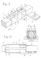
- Fig. 1 shows a preferred embodiment of the press-fit mounting section of an electrical contact according to the invention wherein the mounting section as a whole is illustrated and designated with the reference number 1.
- the contact may have any shape known or used in the art such as a pin contact, bus contact, plug contact,or the like, or their combinations (not shown).
- the mounting section 1 can be located at one end of the contact or between its ends.
- the fins 4 are appropriately clamped down to the base portion 3.
- the fins 4 are formed with reduced thickness, narrowing down in width as well as in thickness towards the base portion for easier insertion of the mounting section 1 in an opening.
- the fins 4 are welded in place near this narrow end 7 of the base portion 3 preferably by means of a laser beam or electrically.
- the fins 4 define in relation to the circumference of the base portion 3 spaces 8 in its longitudinal direction.
- the longitudinal edges of the fins 4 are rounded off on the side facing the wall of the opening and away from the base portion 3.
- the contours of the cross-section of the fins 4 are also shown in Fig. 1 by the dashed lines.
- Fig. 2 shows a longitudinal view along line II-II of the mounting seciton shown in Fig. 1.
- the fins 4 which are formed, for example, by punching from a carrier strip 5 are still connected to the carrier strip 5 via a transfer edge 9.
- the material forming the fins 4 therefore surround the base portion 3 at its end 6 on three sides, with the transfer edge 9 along the bottom. Since the fins 4 are clamped at the end 6 around the base portion 3, the contacts consequently remain attached to the carrier strip 5 via bottom edge 9. From a mounting viewpoint, this is advantageous since several contact elements having a mutual disatnce or pitch corresponding to the mounting holes in a substrate can then be mounted together simultaneously while attached to the carrier strip.
- contacts can be provided for a reliable and mechanically firm mounting in substrate openings having a diameter in the order of magnitude of 0.6 mm or less.
- square wires 0.4 mm wide on a side with fins 0.6 mm wide and having a thickness of 0.12 mm can be used. Fins having such dimensions readily be produced from rolled sheet material with a tolerance of only several micrometers. It is extremely difficult to achieve such tolerances by stamping. Quite obviously. both larger and smaller dimensions are possible, adapted to the specific dimensions of the mounting opening.
- the contact's mounting section comprising the square wire and the fins can be selected of different material, it is possible, in contradistinction with currently available press-fit terminals made from one type of material by stamping, to readily meet special requirements in relation to electrical and mechanical properties.
- a preferred choice of material is a contact made of brass which provides for a sufficient mechanical strength and electrical conductivity and fins made of phosphor bronze or an alloy of beryllium and copper which have the desired spring characteristics and bending properties for an easy and firm mounting in an opening of a substrate.
- the invention is not limited to the demonstrated and discussed preferred embodiments but can be provided in different variations, for example, with more than two fins disposed along the circumference of the base portion with fins twisted in longitudinal direction in relation to each other, with a base portion having a cross-section deviating from the shown angular elliptical shape, etc.
- the use of square wires as a starting material of course is not a necessity and neither is the provision of the contact mounted on a carrier strip.
- the fins may, for example, be welded or soldered over their entire length to the base portion or be clamped, welded or soldered at both ends. Other variations and modifications are possible without departing from the spirit and scope of the present invention.
Landscapes
- Engineering & Computer Science (AREA)
- Manufacturing & Machinery (AREA)
- Coupling Device And Connection With Printed Circuit (AREA)
- Multi-Conductor Connections (AREA)
- Manufacturing Of Electrical Connectors (AREA)
- Connector Housings Or Holding Contact Members (AREA)
- Manufacture Of Switches (AREA)
Applications Claiming Priority (2)
| Application Number | Priority Date | Filing Date | Title |
|---|---|---|---|
| NL8802705A NL8802705A (nl) | 1988-11-03 | 1988-11-03 | Elektrisch contactelement met een montagegedeelte voor montage in een opening van een substraat, alsmede werkwijze voor het van een dergelijk montagegedeelte voorzien van een elektrisch contactelement. |
| NL8802705 | 1988-11-03 |
Publications (2)
| Publication Number | Publication Date |
|---|---|
| EP0367309A1 true EP0367309A1 (fr) | 1990-05-09 |
| EP0367309B1 EP0367309B1 (fr) | 1995-02-15 |
Family
ID=19853165
Family Applications (1)
| Application Number | Title | Priority Date | Filing Date |
|---|---|---|---|
| EP89201587A Expired - Lifetime EP0367309B1 (fr) | 1988-11-03 | 1989-06-16 | Broche électrique à insertion en force |
Country Status (13)
| Country | Link |
|---|---|
| US (1) | US4954104A (fr) |
| EP (1) | EP0367309B1 (fr) |
| JP (1) | JPH02152174A (fr) |
| KR (1) | KR900008730A (fr) |
| CN (1) | CN1042451A (fr) |
| AT (1) | ATE118657T1 (fr) |
| AU (1) | AU614632B2 (fr) |
| BR (1) | BR8903206A (fr) |
| CA (1) | CA1307034C (fr) |
| DE (1) | DE68921143T2 (fr) |
| HK (1) | HK101995A (fr) |
| IL (1) | IL90691A0 (fr) |
| NL (1) | NL8802705A (fr) |
Families Citing this family (4)
| Publication number | Priority date | Publication date | Assignee | Title |
|---|---|---|---|---|
| US5061209A (en) * | 1991-03-13 | 1991-10-29 | Hubbell Incorporated | Wall plate jack and contact therefor |
| JPH0981016A (ja) * | 1995-09-19 | 1997-03-28 | Fujitsu Ltd | 電子写真画像形成装置 |
| TW566695U (en) * | 2003-04-11 | 2003-12-11 | Hon Hai Prec Ind Co Ltd | Electrical connector contact |
| FR2877865B1 (fr) * | 2004-11-15 | 2008-06-06 | Valeo Electronique Sys Liaison | Procede de soudure sans apport de matiere et dispositif electrique susceptible d'etre realise par ce procede |
Citations (3)
| Publication number | Priority date | Publication date | Assignee | Title |
|---|---|---|---|---|
| DE3120629A1 (de) * | 1981-05-23 | 1982-12-23 | Bunker Ramo Corp., 60521 Oak Brook, Ill. | Elektrisches kontaktelement zum einsetzen in eine metallisierte bohrung einer dielektrischen traegerplatte |
| EP0101782A2 (fr) * | 1982-07-30 | 1984-03-07 | Otto Bihler | Ensemble de petit format formant broche de contact |
| US4681392A (en) * | 1986-04-21 | 1987-07-21 | Bead Chain Manufacturing Company | Swaged compliant connector pins for printed circuit boards |
Family Cites Families (6)
| Publication number | Priority date | Publication date | Assignee | Title |
|---|---|---|---|---|
| US4186982A (en) * | 1973-08-01 | 1980-02-05 | Amp Incorporated | Contact with split portion for engagement with substrate |
| US4017143A (en) * | 1975-12-16 | 1977-04-12 | Litton Systems, Inc. | Solderless electrical contact |
| US4274699A (en) * | 1978-04-27 | 1981-06-23 | E. I. Du Pont De Nemours And Company | Press fit terminal with spring arm contact for edgecard connector |
| DE3266605D1 (en) * | 1981-03-02 | 1985-11-07 | Thaler Harmuth F | Pressurized connection pin |
| ATE17415T1 (de) * | 1982-03-04 | 1986-01-15 | Du Pont | Durch einpressen zu befestigende elektrische anschluesse. |
| NL8502046A (nl) * | 1985-07-16 | 1987-02-16 | Du Pont Nederland | Elektrische contactpen voor printplaat. |
-
1988
- 1988-11-03 NL NL8802705A patent/NL8802705A/nl not_active Application Discontinuation
-
1989
- 1989-06-16 DE DE68921143T patent/DE68921143T2/de not_active Expired - Fee Related
- 1989-06-16 EP EP89201587A patent/EP0367309B1/fr not_active Expired - Lifetime
- 1989-06-16 AT AT89201587T patent/ATE118657T1/de not_active IP Right Cessation
- 1989-06-20 AU AU36596/89A patent/AU614632B2/en not_active Ceased
- 1989-06-20 IL IL90691A patent/IL90691A0/xx unknown
- 1989-06-28 CA CA000604220A patent/CA1307034C/fr not_active Expired - Lifetime
- 1989-06-29 BR BR898903206A patent/BR8903206A/pt unknown
- 1989-07-04 JP JP1172832A patent/JPH02152174A/ja active Pending
- 1989-07-12 KR KR1019890009925A patent/KR900008730A/ko not_active Ceased
- 1989-07-21 CN CN89106070A patent/CN1042451A/zh active Pending
-
1990
- 1990-02-08 US US07/477,179 patent/US4954104A/en not_active Expired - Fee Related
-
1995
- 1995-06-22 HK HK101995A patent/HK101995A/en not_active IP Right Cessation
Patent Citations (3)
| Publication number | Priority date | Publication date | Assignee | Title |
|---|---|---|---|---|
| DE3120629A1 (de) * | 1981-05-23 | 1982-12-23 | Bunker Ramo Corp., 60521 Oak Brook, Ill. | Elektrisches kontaktelement zum einsetzen in eine metallisierte bohrung einer dielektrischen traegerplatte |
| EP0101782A2 (fr) * | 1982-07-30 | 1984-03-07 | Otto Bihler | Ensemble de petit format formant broche de contact |
| US4681392A (en) * | 1986-04-21 | 1987-07-21 | Bead Chain Manufacturing Company | Swaged compliant connector pins for printed circuit boards |
Also Published As
| Publication number | Publication date |
|---|---|
| BR8903206A (pt) | 1990-09-25 |
| NL8802705A (nl) | 1990-06-01 |
| US4954104A (en) | 1990-09-04 |
| JPH02152174A (ja) | 1990-06-12 |
| CN1042451A (zh) | 1990-05-23 |
| DE68921143T2 (de) | 1995-09-07 |
| DE68921143D1 (de) | 1995-03-23 |
| HK101995A (en) | 1995-06-30 |
| AU614632B2 (en) | 1991-09-05 |
| ATE118657T1 (de) | 1995-03-15 |
| AU3659689A (en) | 1990-05-10 |
| IL90691A0 (en) | 1990-01-18 |
| EP0367309B1 (fr) | 1995-02-15 |
| CA1307034C (fr) | 1992-09-01 |
| KR900008730A (ko) | 1990-06-04 |
Similar Documents
| Publication | Publication Date | Title |
|---|---|---|
| US4017143A (en) | Solderless electrical contact | |
| JP2803574B2 (ja) | コネクタのプレスイン端子及びその製造方法 | |
| US6042429A (en) | Continuous press-fit knurl pin | |
| US4679889A (en) | Solder-bearing leads | |
| US4469394A (en) | Press-fit electrical terminals | |
| US5897401A (en) | Serrated starred pin | |
| JPS6391972A (ja) | プリント基板用端子 | |
| JPH08508613A (ja) | ばね偏倚式テーパー付き接点要素 | |
| JPS6221255A (ja) | プリント回路基板用の電気コンタクトピン | |
| US5915999A (en) | Press-fit connecting pin and electronic device using the same | |
| US3681744A (en) | Circuit board socket | |
| US6406338B1 (en) | Board terminal and method of producing same | |
| US4723923A (en) | Low insertion, stamped and formed contact sleeve | |
| US5688150A (en) | Solder bearing lead | |
| US4954104A (en) | Press-fit electrical terminal | |
| EP0807325B1 (fr) | Broches de connexion s'emmanchant a force et dispositif electronique les utilisant | |
| US20020002007A1 (en) | Board terminal and method of producing same | |
| GB2195836A (en) | Contact pin | |
| CN100423372C (zh) | 插入组件及在绝缘板里形成和装载金属弹簧触头的方法 | |
| US20010046817A1 (en) | Compliant pin and its method of manufacture | |
| WO1994024730A1 (fr) | Element de blocage pour composants electriques et/ou electroniques | |
| KR100236434B1 (ko) | 둥근 납땜 미부를 갖는 전기 커넥터 단자(electric connector terminal having a round soldering tail) | |
| US20050042935A1 (en) | Solderless electrical contact | |
| US6203386B1 (en) | Terminal blades mounted on flexible substrates | |
| KR20050050581A (ko) | 억지 끼워맞춤용 컨택트 및 이것을 이용한 억지 끼워맞춤커넥터 |
Legal Events
| Date | Code | Title | Description |
|---|---|---|---|
| PUAI | Public reference made under article 153(3) epc to a published international application that has entered the european phase |
Free format text: ORIGINAL CODE: 0009012 |
|
| AK | Designated contracting states |
Kind code of ref document: A1 Designated state(s): AT BE CH DE ES FR GB IT LI LU NL SE |
|
| 17P | Request for examination filed |
Effective date: 19901029 |
|
| 17Q | First examination report despatched |
Effective date: 19930920 |
|
| RAP1 | Party data changed (applicant data changed or rights of an application transferred) |
Owner name: CONNECTOR SYSTEMS TECHNOLOGY N.V. Owner name: DU PONT DE NEMOURS (NEDERLAND) B.V. |
|
| GRAA | (expected) grant |
Free format text: ORIGINAL CODE: 0009210 |
|
| AK | Designated contracting states |
Kind code of ref document: B1 Designated state(s): AT BE CH DE ES FR GB IT LI LU NL SE |
|
| PG25 | Lapsed in a contracting state [announced via postgrant information from national office to epo] |
Ref country code: IT Free format text: LAPSE BECAUSE OF FAILURE TO SUBMIT A TRANSLATION OF THE DESCRIPTION OR TO PAY THE FEE WITHIN THE PRESCRIBED TIME-LIMIT;WARNING: LAPSES OF ITALIAN PATENTS WITH EFFECTIVE DATE BEFORE 2007 MAY HAVE OCCURRED AT ANY TIME BEFORE 2007. THE CORRECT EFFECTIVE DATE MAY BE DIFFERENT FROM THE ONE RECORDED. Effective date: 19950215 Ref country code: LI Effective date: 19950215 Ref country code: NL Effective date: 19950215 Ref country code: CH Effective date: 19950215 Ref country code: ES Free format text: THE PATENT HAS BEEN ANNULLED BY A DECISION OF A NATIONAL AUTHORITY Effective date: 19950215 Ref country code: BE Effective date: 19950215 Ref country code: AT Effective date: 19950215 |
|
| REF | Corresponds to: |
Ref document number: 118657 Country of ref document: AT Date of ref document: 19950315 Kind code of ref document: T |
|
| ET | Fr: translation filed | ||
| REF | Corresponds to: |
Ref document number: 68921143 Country of ref document: DE Date of ref document: 19950323 |
|
| PG25 | Lapsed in a contracting state [announced via postgrant information from national office to epo] |
Ref country code: SE Effective date: 19950515 |
|
| REG | Reference to a national code |
Ref country code: CH Ref legal event code: PL |
|
| PGFP | Annual fee paid to national office [announced via postgrant information from national office to epo] |
Ref country code: FR Payment date: 19950616 Year of fee payment: 7 |
|
| PGFP | Annual fee paid to national office [announced via postgrant information from national office to epo] |
Ref country code: DE Payment date: 19950629 Year of fee payment: 7 |
|
| PG25 | Lapsed in a contracting state [announced via postgrant information from national office to epo] |
Ref country code: LU Free format text: LAPSE BECAUSE OF NON-PAYMENT OF DUE FEES Effective date: 19950630 |
|
| NLV1 | Nl: lapsed or annulled due to failure to fulfill the requirements of art. 29p and 29m of the patents act | ||
| PLBE | No opposition filed within time limit |
Free format text: ORIGINAL CODE: 0009261 |
|
| STAA | Information on the status of an ep patent application or granted ep patent |
Free format text: STATUS: NO OPPOSITION FILED WITHIN TIME LIMIT |
|
| 26N | No opposition filed | ||
| PG25 | Lapsed in a contracting state [announced via postgrant information from national office to epo] |
Ref country code: FR Effective date: 19970228 |
|
| PG25 | Lapsed in a contracting state [announced via postgrant information from national office to epo] |
Ref country code: DE Effective date: 19970301 |
|
| REG | Reference to a national code |
Ref country code: FR Ref legal event code: ST |
|
| REG | Reference to a national code |
Ref country code: GB Ref legal event code: 732E |
|
| PGFP | Annual fee paid to national office [announced via postgrant information from national office to epo] |
Ref country code: GB Payment date: 20010502 Year of fee payment: 13 |
|
| REG | Reference to a national code |
Ref country code: GB Ref legal event code: IF02 |
|
| PG25 | Lapsed in a contracting state [announced via postgrant information from national office to epo] |
Ref country code: GB Free format text: LAPSE BECAUSE OF NON-PAYMENT OF DUE FEES Effective date: 20020616 |
|
| GBPC | Gb: european patent ceased through non-payment of renewal fee |
Effective date: 20020616 |