EP0367311B1 - Procédé de montage d'un composant électronique et carte à mémoire en faisant usage - Google Patents
Procédé de montage d'un composant électronique et carte à mémoire en faisant usage Download PDFInfo
- Publication number
- EP0367311B1 EP0367311B1 EP89202342A EP89202342A EP0367311B1 EP 0367311 B1 EP0367311 B1 EP 0367311B1 EP 89202342 A EP89202342 A EP 89202342A EP 89202342 A EP89202342 A EP 89202342A EP 0367311 B1 EP0367311 B1 EP 0367311B1
- Authority
- EP
- European Patent Office
- Prior art keywords
- layer
- conductive
- hole
- card
- electronic component
- Prior art date
- Legal status (The legal status is an assumption and is not a legal conclusion. Google has not performed a legal analysis and makes no representation as to the accuracy of the status listed.)
- Expired - Lifetime
Links
Images
Classifications
-
- G—PHYSICS
- G06—COMPUTING OR CALCULATING; COUNTING
- G06K—GRAPHICAL DATA READING; PRESENTATION OF DATA; RECORD CARRIERS; HANDLING RECORD CARRIERS
- G06K19/00—Record carriers for use with machines and with at least a part designed to carry digital markings
- G06K19/06—Record carriers for use with machines and with at least a part designed to carry digital markings characterised by the kind of the digital marking, e.g. shape, nature, code
- G06K19/067—Record carriers with conductive marks, printed circuits or semiconductor circuit elements, e.g. credit or identity cards also with resonating or responding marks without active components
- G06K19/07—Record carriers with conductive marks, printed circuits or semiconductor circuit elements, e.g. credit or identity cards also with resonating or responding marks without active components with integrated circuit chips
- G06K19/077—Constructional details, e.g. mounting of circuits in the carrier
- G06K19/07745—Mounting details of integrated circuit chips
-
- H—ELECTRICITY
- H05—ELECTRIC TECHNIQUES NOT OTHERWISE PROVIDED FOR
- H05K—PRINTED CIRCUITS; CASINGS OR CONSTRUCTIONAL DETAILS OF ELECTRIC APPARATUS; MANUFACTURE OF ASSEMBLAGES OF ELECTRICAL COMPONENTS
- H05K1/00—Printed circuits
- H05K1/18—Printed circuits structurally associated with non-printed electric components
- H05K1/182—Printed circuits structurally associated with non-printed electric components associated with components mounted in printed circuit boards [PCB], e.g. insert-mounted components [IMC]
-
- H—ELECTRICITY
- H05—ELECTRIC TECHNIQUES NOT OTHERWISE PROVIDED FOR
- H05K—PRINTED CIRCUITS; CASINGS OR CONSTRUCTIONAL DETAILS OF ELECTRIC APPARATUS; MANUFACTURE OF ASSEMBLAGES OF ELECTRICAL COMPONENTS
- H05K3/00—Apparatus or processes for manufacturing printed circuits
- H05K3/02—Apparatus or processes for manufacturing printed circuits in which the conductive material is applied to the surface of the insulating support and is thereafter removed from such areas of the surface which are not intended for current conducting or shielding
- H05K3/06—Apparatus or processes for manufacturing printed circuits in which the conductive material is applied to the surface of the insulating support and is thereafter removed from such areas of the surface which are not intended for current conducting or shielding the conductive material being removed chemically or electrolytically, e.g. by photo-etch process
-
- H—ELECTRICITY
- H05—ELECTRIC TECHNIQUES NOT OTHERWISE PROVIDED FOR
- H05K—PRINTED CIRCUITS; CASINGS OR CONSTRUCTIONAL DETAILS OF ELECTRIC APPARATUS; MANUFACTURE OF ASSEMBLAGES OF ELECTRICAL COMPONENTS
- H05K3/00—Apparatus or processes for manufacturing printed circuits
- H05K3/30—Assembling printed circuits with electric components, e.g. with resistors
- H05K3/32—Assembling printed circuits with electric components, e.g. with resistors electrically connecting electric components or wires to printed circuits
- H05K3/328—Assembling printed circuits with electric components, e.g. with resistors electrically connecting electric components or wires to printed circuits by welding
-
- H—ELECTRICITY
- H10—SEMICONDUCTOR DEVICES; ELECTRIC SOLID-STATE DEVICES NOT OTHERWISE PROVIDED FOR
- H10W—GENERIC PACKAGES, INTERCONNECTIONS, CONNECTORS OR OTHER CONSTRUCTIONAL DETAILS OF DEVICES COVERED BY CLASS H10
- H10W72/00—Interconnections or connectors in packages
- H10W72/071—Connecting or disconnecting
- H10W72/072—Connecting or disconnecting of bump connectors
- H10W72/07231—Techniques
- H10W72/07236—Soldering or alloying
-
- Y—GENERAL TAGGING OF NEW TECHNOLOGICAL DEVELOPMENTS; GENERAL TAGGING OF CROSS-SECTIONAL TECHNOLOGIES SPANNING OVER SEVERAL SECTIONS OF THE IPC; TECHNICAL SUBJECTS COVERED BY FORMER USPC CROSS-REFERENCE ART COLLECTIONS [XRACs] AND DIGESTS
- Y10—TECHNICAL SUBJECTS COVERED BY FORMER USPC
- Y10T—TECHNICAL SUBJECTS COVERED BY FORMER US CLASSIFICATION
- Y10T29/00—Metal working
- Y10T29/49—Method of mechanical manufacture
- Y10T29/49002—Electrical device making
- Y10T29/49117—Conductor or circuit manufacturing
- Y10T29/49124—On flat or curved insulated base, e.g., printed circuit, etc.
- Y10T29/4913—Assembling to base an electrical component, e.g., capacitor, etc.
- Y10T29/49144—Assembling to base an electrical component, e.g., capacitor, etc. by metal fusion
Definitions
- the present invention relates to a method for mounting an electronic component into a card and for interconnecting them, said electronic component being provided with at least one conductive bump constituting a terminal thereof, said method including the steps of creating at least one hole into said card, covering one end of said hole and at least that part of said card surrounding said hole by a layer of a conductive material, mounting said component into said hole of said card and interconnecting said conductive bump and a portion of the adjacent one side of said layer.
- the wire bonding method provides an high bonding flexibility but requires two wire bonding operations : a first one to connect one end of a wire with the conductive bump and a second one to connect the other end of the wire with the conductive portion of the card.
- This wire as well as the bonds themselves constitute unwanted conduction resistances.
- it is not easy to realize a relatively flat interconnection and to obtain plastic memory cards of the "credit" type realized according to the International Standards Organization (ISO) recommendations, i.e. having a small height.
- ISO International Standards Organization
- TAB Tape Automated Bonding
- the Printed Wiring Connection (PWC) method consists in successively mounting the electronic component, more particularly a Large Scale Integrated (LSI) chip, into the hole, embedding this chip in the hole, and realizing the interconnections by screen printing a pattern of conductive polymeric paste on the card through a mask.
- This method has several advantages since the interconnection realized has a small height and a low conduction resistance, but a drawback thereof is that the position of the chip in the hole and more particularly of each conductive bump thereof is not accurately known so that correctly positioning the mask for screen printing is a problem.
- An object of the present invention is to provide a method which has the last mentioned advantages and moreover allows the position of the conductive bump in the hole to be accurately known.
- this object is achieved due to the fact that said interconnection is realized by pressing said electronic component and said one side of said conductive layer against each other so that the profile of said conductive bump protrudes from the other side of said layer.
- the protrusion or convex bump created by the conductive bump of the electronic component on the external surface of the conductive layer allows to accurately know the position of this corresponding conductive bump and thus also of the electronic component facilitating thereby a subsequent alignment operation, e.g. a screen printing operation.
- Another characteristic feature of the present method is that during the interconnection step said conductive bump is soldered to said conductive layer by heating said conductive layer, said electronic component, or both.
- the European Patent Application EP-A1-0207852 also discloses a method of the type described above. Therein, protrusions directed towards the electronic component are created in the conductive layer in order to realize the interconnection. Also here this is not an easy operation since the position of the electronic component and more particularly of the conductive bumps thereof are not exactly known as they are not visible through the conductive layer covering the hole. Other methods are also known from the European Patent Application EP-A1-0 207 853 and from the French Patent Application FR-A-2 601 477.
- Still another characteristic feature of the present method is that during the interconnection step portions are removed from said conductive layer.
- these portions are removed from said conductive layer by an etching technique similar to the one used to realize printed circuit boards.
- the realized interconnection does not increase the thickness of the card and the conduction resistance introduced by the contact is very small.
- the present method also relates to a process for creating a conductive bump on a terminal pad of an integrated electronic component coated with a passivation layer.
- the terminal pads are located in recesses of the passivation layer so that their interconnection with an above mentioned card by the above method or by the printed wiring connection (PWC) is impossible.
- Another object of the present method is to provide a process for creating a conductive bump protruding from the passivation layer so that the above method according to the invention may be used for interconnecting the electronic component and a card.
- this other object is achieved due to the fact that said process includes the steps of covering said passivation layer with a conductive protection layer, of covering said protection layer with a mask having a hole at a location corresponding to said terminal pad, of depositing a metal into said hole, of removing said mask, and of etching said protection layer so as to remove the portions thereof covering said passivation layer.
- a conductive bump is created at the location of the terminal pad of the electronic component and protrudes from the passivation layer.
- IC Integrated Circuit
- memory card when able to store variable data or intelligent (smart) card when including a microprocessor.
- IC Integrated Circuit
- it also houses a number of electronic components such as a battery, a Random Access Memory (RAM), a Read-Only Memory (ROM) and/or other Large Scale Integrated (LSI) chips connected to terminals of a circuit printed on the card.
- RAM Random Access Memory
- ROM Read-Only Memory
- LSI Large Scale Integrated
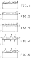
- Fig. 1 shows an LSI chip 1 having terminal pads 6, 7, 8 located in recesses or holes of a passivation layer 9 covering the upper surface of the chip 1.
- the passivation layer 9 is for instance a layer of silicon nitride and its goal is to protect the chip 1 against corrosion and other possible damages.
- a trimetal layer 10 is deposited over the passivation layer 9.
- This layer 10 is constituted by titanium, tungsten and gold.
- the process to apply such a trimetal layer 10 on a passivation layer 9 is for instance described in the article "STUDIES OF THE Ti-W/Au METALLIZATION ON ALUMINUM" by R. NOWICKI et al, published at the occasion of the "International Conference on Metallurgical Coatings", San Francisco, California, U.S.A., April 3-7, 1978, pages 195 to 205.
- This trimetal layer 10 has a thickness of about 2,000 Angström.
- Fig. 3 illustrates a second step of the present process which consists in covering the trimetal layer 10 with a photolithographic mask 11.
- This photolithographic mask 11 is such that the trimetal layer 10 is accessible through holes 12, 13, 14 corresponding to the locations of the terminal pads 6, 7, 8 respectively.
- a third process step consists in sputtering in the holes 12, 13, 14 metallic material which is for instance gold or copper.
- Electrically conductive bumps 2, 3, 4 are created in this manner at the locations of the terminal pads 6, 7, 8 of the chip 1 respectively. These conductive bumps 2, 3, 4 have a height of about 25 to 30 microns.
- a fourth process step illustrated by Fig. 5 first the photolithographic mask 11 is removed from the chip 1 and the latter is etched to remove the portions of the trimetal layer 10 covering the passivation layer 9. Because the thickness of the trimetal layer 10 is much smaller than the height of the conductive bumps 2, 3, 4, the latter are only sligthly affected by this metal etching process.
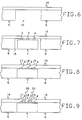
- a first method step related to Fig. 6, consists in making one or more holes 15 in the card 5.
- the hole 15 is slightly larger than and has the same shape, e.g. rectangular, as the LSI chip 1 to be mounted therein.
- the whole card 5 including the hole 15 is covered with a layer 16 of an electrically conductive material which is generally a metal such as copper or a metallic alloy such as brass.
- the chip 1 is mounted inside the hole 15 so that the conductive bumps 2, 3, 4 thereof make contact with the conductive layer 16 covering the hole 15.
- the chip 1 is therefore first mounted on a support which brings it into the hole 15 or, in a preferred embodiment (not shown), the card 5 is reversed and the chip 1 is handled by suction means which positions it into the hole 15.
- a fourth method step an intimate electrical contact is ensured between the conductive bumps 2, 3, 4 and the conductive layer 16 by exerting pressure on the chip 1 towards the conductive layer 16 while heating either the chip 1, the conductive layer 16, or both so as to perform a contact soldering.
- a "thermode” is placed on the chip 1 to simultaneously create pressure and heating. By this operation the conductive bumps 2, 3, 4 create protrusions 17, 18, 19 on the upper surface of the conductive layer 16 respectively.
- a layer of material such as tin may be coated on the lower side of the portion of conductive layer 16 which covers this hole 15 in order to facilitate the soldering of the conductive bumps 2, 3, 4 to this layer 16.
- the chip 1 is embedded in the hole 15 by filling it (not shown) with an embedding material such as epoxy.
- the embedding material has a viscosity which allows it to fill the interstices between the chip 1 and the layer 16.
- the coefficient of expansion of the embedding material is chosen so that the card 5 is not mechanically affected by the heat dissipation of the operating chip 1.
- the bottom side of the card 5 is then laminated to obtain the planar structure shown in Fig. 8.
- Fig. 9 relates to a sixth and last method step which consists in etching the conductive layer 16 to obtain a required circuit pattern on the upper surface of the smart card.
- the protrusions 17, 18, 19 on the upper surface of the conductive layer 16 thereby facilitate the alignment of the etching mask as they allow a visual localization of the conductive bumps 2, 3, 4 of the chip 1.
- Portions 20 and 21 can thus be removed from the electrically conductive layer 16 with an high accuracy.
- the width of the paths of the conductive layer 16 remaining after the portions 20, 21 have been removed and interconnecting the chip 1 and the card 5 is chosen in function of the value of the current which has to flow therethrough or of the type of connection path required, e.g. a wide ground connection path as compared to a smaller signal connection path.
- the smart card thus obtained may afterwards be coated with a layer of protective and/or strengthening material.
- the terminal pads 6, 7, 8 of the chip 1 need no longer be exclusively located at the periphery thereof as it is the case for instance when the wire bonding method is used. If in this case a terminal pad is not located at the periphery, the interconnecting wires then extend over the chip 1 and may be displaced, e.g. by vibrations, thereby causing short-circuits or at least constituting variable capacitances with this chip.
- Another application of the present method is to create a heat dissipation element for the chip 1. Since the portion of the surface of the chip 1 which has the highest power dissipation can be determined, terminal pads of the same type as 6, 7, 8 may be created near this portion and connected to a portion of the layer 16 via heat conductive bumps of the same type as 2, 3, 4. This portion of the layer 16 may be chosen sufficiently large to operate as a heating dissipation element.
Landscapes
- Engineering & Computer Science (AREA)
- Computer Hardware Design (AREA)
- Microelectronics & Electronic Packaging (AREA)
- Physics & Mathematics (AREA)
- General Physics & Mathematics (AREA)
- Theoretical Computer Science (AREA)
- Credit Cards Or The Like (AREA)
- Holo Graphy (AREA)
- Electrically Operated Instructional Devices (AREA)
- Wire Bonding (AREA)
Claims (10)
- Procédé de montage d'un composant électronique (1) dans une carte (5) et d'interconnexion de ces deux éléments, ledit composant électronique étant équipé d'au moins une bosse conductrice (2, 3, 4) qui en constitue une plage de connexion (6, 7, 8), ledit procédé incluant les opérations de création d'au moins un trou (15) dans ladite carte (5), de revêtement d'une extrémité dudit trou (15) et d'au moins la partie de ladite carte (5) entourant ledit trou avec une couche de matériau conducteur (16), de montage dudit composant (1) dans ledit trou (15) de ladite carte (5) et d'interconnexion de ladite bosse conductrice (2, 3, 4) et d'une partie de la face adjacente de ladite couche (16), ladite interconnexion étant réalisée en pressant ledit composant électronique (1) et ladite face de ladite couche conductrice (16) l'un contre l'autre, caractérisé par le fait que le profil de ladite bosse conductrice (2, 3, 4) fait saillie sur l'autre face de ladite couche (16).
- Procédé conforme à la revendication 1, caractérisé par le fait que dans l'étape d'interconnexion, ladite bosse conductrice (2, 3, 4) est soudée à ladite couche conductrice (16) en chauffant ladite couche conductrice.
- Procédé conforme à la revendication 1, caractérisé par le fait que dans l'étape d'interconnexion, ladite bosse conductrice (2, 3, 4) est soudée à ladite couche conductrice (16) en chauffant ledit composant électronique (1).
- Procédé conforme à la revendication 2 ou 3, caractérisé par le fait qu'un métal intermédiaire (Sn), est interposé entre ladite bosse conductrice (2, 3, 4) et ladite couche conductrice (16) pour faciliter ladite opération de soudage.
- Procédé conforme à la revendication 1, caractérisé par le fait que, dans l'étape d'interconnexion, des parties (20, 21) sont enlevées de ladite couche conductrice (16).
- Procédé conforme à la revendication 5, caractérisé par le fait que lesdites parties (20, 21) sont enlevées de ladite couche conductrice (16) par attaque chimique.
- Procédé conforme à la revendication 2 ou 3 et à la revendication 5, caractérisé par le fait que lesdites parties (20, 21) sont enlevées de ladite couche conductrice (16) après ladite opération de soudage.
- Procédé conforme à la revendication 1, caractérisé par le fait que ladite bosse conductrice (2, 3, 4) et ladite couche conductrice (16) sont toutes deux conductrices de la chaleur ainsi que de l'électricité.
- Procédé conforme à la revendication 1, caractérisé par le fait que ladite couche conductrice (16) est une couche métallique.
- Procédé conforme à la revendication 1, caractérisé par le fait que la création de ladite bosse conductrice (2, 3, 4) sur ledit composant électronique (1) comporte les étapes de revêtement dudit composant par une couche de passivation (9), de revêtement de ladite couche de passivation (8) par une couche de protection conductrice (10), de revêtement de ladite couche de protection par un masque (11) comportant un trou (12, 13, 14) à l'emplacement correspondant à ladite plage de connexion (6, 7, 8), de dépôt d'un métal dans ledit trou, d'enlèvement dudit masque et d'attaque chimique de ladite couche de protection (10) de manière à enlever les parties de cette couche qui couvrent ladite couche de passivation.
Priority Applications (1)
| Application Number | Priority Date | Filing Date | Title |
|---|---|---|---|
| AT89202342T ATE93075T1 (de) | 1988-09-27 | 1989-09-16 | Verfahren zum montieren eines elektronischen bausteins und diesen verwendende speicherkarte. |
Applications Claiming Priority (2)
| Application Number | Priority Date | Filing Date | Title |
|---|---|---|---|
| BE8801103A BE1002529A6 (nl) | 1988-09-27 | 1988-09-27 | Methode om een elektronische component te monteren en geheugen kaart waarin deze wordt toegepast. |
| BE8801103 | 1988-09-27 |
Publications (2)
| Publication Number | Publication Date |
|---|---|
| EP0367311A1 EP0367311A1 (fr) | 1990-05-09 |
| EP0367311B1 true EP0367311B1 (fr) | 1993-08-11 |
Family
ID=3883649
Family Applications (1)
| Application Number | Title | Priority Date | Filing Date |
|---|---|---|---|
| EP89202342A Expired - Lifetime EP0367311B1 (fr) | 1988-09-27 | 1989-09-16 | Procédé de montage d'un composant électronique et carte à mémoire en faisant usage |
Country Status (7)
| Country | Link |
|---|---|
| US (1) | US5042145A (fr) |
| EP (1) | EP0367311B1 (fr) |
| AT (1) | ATE93075T1 (fr) |
| AU (2) | AU617867B2 (fr) |
| BE (1) | BE1002529A6 (fr) |
| DE (1) | DE68908341T2 (fr) |
| ES (1) | ES2044061T3 (fr) |
Families Citing this family (20)
| Publication number | Priority date | Publication date | Assignee | Title |
|---|---|---|---|---|
| US5203078A (en) * | 1985-07-17 | 1993-04-20 | Ibiden Co., Ltd. | Printed wiring board for IC cards |
| US5274570A (en) * | 1989-05-22 | 1993-12-28 | Mazda Motor Corporation | Integrated circuit having metal substrate |
| JPH06511581A (ja) * | 1992-05-25 | 1994-12-22 | ガイ フレール バーント エ エクスポルタシオン ソシエテ アノニム | 電子ラベル |
| DE4424396C2 (de) * | 1994-07-11 | 1996-12-12 | Ibm | Trägerelement zum Einbau in Chipkarten oder anderen Datenträgerkarten |
| FR2731132B1 (fr) * | 1995-02-24 | 1997-04-04 | Solaic Sa | Procede pour implanter un element electronique, notamment un microcircuit, dans un corps de carte electronique, et corps de carte electronique comportant un element electronique ainsi implante |
| SE9701612D0 (sv) | 1997-04-29 | 1997-04-29 | Johan Asplund | Smartcard and method for its manufacture |
| US6531997B1 (en) | 1999-04-30 | 2003-03-11 | E Ink Corporation | Methods for addressing electrophoretic displays |
| EP1990832A3 (fr) * | 2000-02-25 | 2010-09-29 | Ibiden Co., Ltd. | Carte de circuit imprimé multicouche et son procédé de fabrication |
| WO2002027786A1 (fr) | 2000-09-25 | 2002-04-04 | Ibiden Co., Ltd. | Element semi-conducteur, procede de fabrication d'un element semi-conducteur, carte a circuit imprime multicouche, et procede de fabrication d'une carte a circuit imprime multicouche |
| US7140540B2 (en) * | 2002-05-08 | 2006-11-28 | Lasercard Corporation | Method of making secure personal data card |
| FI20030293A7 (fi) * | 2003-02-26 | 2004-08-27 | Imbera Electronics Oy | Menetelmä elektroniikkamoduulin valmistamiseksi ja elektroniikkamoduuli |
| FI119583B (fi) * | 2003-02-26 | 2008-12-31 | Imbera Electronics Oy | Menetelmä elektroniikkamoduulin valmistamiseksi |
| FI20031341L (fi) | 2003-09-18 | 2005-03-19 | Imbera Electronics Oy | Menetelmä elektroniikkamoduulin valmistamiseksi |
| FI117814B (fi) * | 2004-06-15 | 2007-02-28 | Imbera Electronics Oy | Menetelmä elektroniikkamoduulin valmistamiseksi |
| GB2441265B (en) * | 2005-06-16 | 2012-01-11 | Imbera Electronics Oy | Method for manufacturing a circuit board structure, and a circuit board structure |
| FI122128B (fi) * | 2005-06-16 | 2011-08-31 | Imbera Electronics Oy | Menetelmä piirilevyrakenteen valmistamiseksi |
| FI119714B (fi) | 2005-06-16 | 2009-02-13 | Imbera Electronics Oy | Piirilevyrakenne ja menetelmä piirilevyrakenteen valmistamiseksi |
| FI20060256A7 (fi) * | 2006-03-17 | 2006-03-20 | Imbera Electronics Oy | Piirilevyn valmistaminen ja komponentin sisältävä piirilevy |
| US7836588B2 (en) * | 2006-07-06 | 2010-11-23 | Ideon Llc | Method for fabricating an electronic device |
| GB0705287D0 (en) * | 2007-03-20 | 2007-04-25 | Conductive Inkjet Tech Ltd | Electrical connection of components |
Family Cites Families (10)
| Publication number | Priority date | Publication date | Assignee | Title |
|---|---|---|---|---|
| GB1339660A (en) * | 1971-11-20 | 1973-12-05 | Ferranti Ltd | Supports for semiconductor devices |
| JPS5231673A (en) * | 1975-09-04 | 1977-03-10 | Sharp Corp | Resin sealing method of semiconductor device |
| JPS53149763A (en) * | 1977-06-01 | 1978-12-27 | Citizen Watch Co Ltd | Mounting method of semiconductor integrate circuit |
| DE3248385A1 (de) * | 1982-12-28 | 1984-06-28 | GAO Gesellschaft für Automation und Organisation mbH, 8000 München | Ausweiskarte mit integriertem schaltkreis |
| FR2584235B1 (fr) * | 1985-06-26 | 1988-04-22 | Bull Sa | Procede de montage d'un circuit integre sur un support, dispositif en resultant et son application a une carte a microcircuits electroniques |
| FR2584236B1 (fr) * | 1985-06-26 | 1988-04-29 | Bull Sa | Procede de montage d'un circuit integre sur un support, dispositif en resultant et son application a une carte a microcircuits electroniques |
| JPH074995B2 (ja) * | 1986-05-20 | 1995-01-25 | 株式会社東芝 | Icカ−ド及びその製造方法 |
| FR2601477B1 (fr) * | 1986-07-11 | 1988-10-21 | Bull Cp8 | Procede de montage d'un circuit integre dans une carte a microcircuits electroniques, et carte en resultant |
| FR2625067A1 (fr) * | 1987-12-22 | 1989-06-23 | Sgs Thomson Microelectronics | Procede pour fixer sur un support un composant electronique et ses contacts |
| FR2631200B1 (fr) * | 1988-05-09 | 1991-02-08 | Bull Cp8 | Circuit imprime souple, notamment pour carte a microcircuits electroniques, et carte incorporant un tel circuit |
-
1988
- 1988-09-27 BE BE8801103A patent/BE1002529A6/nl not_active IP Right Cessation
-
1989
- 1989-09-16 ES ES89202342T patent/ES2044061T3/es not_active Expired - Fee Related
- 1989-09-16 DE DE89202342T patent/DE68908341T2/de not_active Expired - Fee Related
- 1989-09-16 AT AT89202342T patent/ATE93075T1/de not_active IP Right Cessation
- 1989-09-16 EP EP89202342A patent/EP0367311B1/fr not_active Expired - Lifetime
- 1989-09-18 AU AU41427/89A patent/AU617867B2/en not_active Ceased
- 1989-12-06 US US07/446,529 patent/US5042145A/en not_active Expired - Fee Related
-
1991
- 1991-08-30 AU AU83531/91A patent/AU646284B2/en not_active Ceased
Also Published As
| Publication number | Publication date |
|---|---|
| AU617867B2 (en) | 1991-12-05 |
| AU4142789A (en) | 1990-04-05 |
| ES2044061T3 (es) | 1994-01-01 |
| BE1002529A6 (nl) | 1991-03-12 |
| DE68908341T2 (de) | 1994-01-13 |
| AU646284B2 (en) | 1994-02-17 |
| EP0367311A1 (fr) | 1990-05-09 |
| DE68908341D1 (de) | 1993-09-16 |
| US5042145A (en) | 1991-08-27 |
| ATE93075T1 (de) | 1993-08-15 |
| AU8353191A (en) | 1991-11-07 |
Similar Documents
| Publication | Publication Date | Title |
|---|---|---|
| EP0367311B1 (fr) | Procédé de montage d'un composant électronique et carte à mémoire en faisant usage | |
| US5200362A (en) | Method of attaching conductive traces to an encapsulated semiconductor die using a removable transfer film | |
| JP3430339B2 (ja) | チップカードまたは類似の電子デバイスの製造方法 | |
| US6358772B2 (en) | Semiconductor package having semiconductor element mounting structure of semiconductor package mounted on circuit board and method of assembling semiconductor package | |
| US5930603A (en) | Method for producing a semiconductor device | |
| KR100445072B1 (ko) | 리드 프레임을 이용한 범프 칩 캐리어 패키지 및 그의제조 방법 | |
| US6191951B1 (en) | Smart card module and smart card including a smart card module | |
| US5407864A (en) | Process for mounting a semiconductor chip and depositing contacts into through holes of a circuit board and of an insulating interposer and onto the chip | |
| US5673478A (en) | Method of forming an electronic device having I/O reroute | |
| HK84095A (en) | Method for mounting an integrated circuit on a support, resultant device and its use in an electronic microcircuit card | |
| EP0459493A2 (fr) | Dispositif semi-conducteur utilisant un cadre conducteur et son procédé de fabrication | |
| US6420787B1 (en) | Semiconductor device and process of producing same | |
| EP0614219A1 (fr) | Technologie d'empaquetage pour une puce semi-conductrice | |
| CN1183486C (zh) | 用于芯片卡的电子组件 | |
| AU735725B2 (en) | Method for making a contactless card with antenna connected with soldered wires | |
| CN100359682C (zh) | 电子标签及其制造方法 | |
| US6414585B1 (en) | Integrated passive components and package with posts | |
| EP0997939A1 (fr) | Dispositif semiconducteur comprenant un fil conducteur | |
| RU2328840C2 (ru) | Способ монтажа электронного компонента на подложке | |
| EP1744362A2 (fr) | Dispositif semiconducteur et appareil électronique | |
| CA2003229C (fr) | Methode de montage d'un element electronique et carte memoire resultante | |
| NZ239815A (en) | Conductive protrusions on integrated electronic components as terminals | |
| NZ230738A (en) | Electronic component mounting on card by conductive pads | |
| US6995082B2 (en) | Bonding pad of a semiconductor device and formation method thereof | |
| EP1854134A2 (fr) | Procede et dispositif de connexion par contact de puces a semi-conducteur sur un substrat metallique |
Legal Events
| Date | Code | Title | Description |
|---|---|---|---|
| PUAI | Public reference made under article 153(3) epc to a published international application that has entered the european phase |
Free format text: ORIGINAL CODE: 0009012 |
|
| AK | Designated contracting states |
Kind code of ref document: A1 Designated state(s): AT BE CH DE ES FR GB IT LI NL SE |
|
| 17P | Request for examination filed |
Effective date: 19901029 |
|
| 17Q | First examination report despatched |
Effective date: 19930126 |
|
| GRAA | (expected) grant |
Free format text: ORIGINAL CODE: 0009210 |
|
| AK | Designated contracting states |
Kind code of ref document: B1 Designated state(s): AT BE CH DE ES FR GB IT LI NL SE |
|
| REF | Corresponds to: |
Ref document number: 93075 Country of ref document: AT Date of ref document: 19930815 Kind code of ref document: T |
|
| ITF | It: translation for a ep patent filed | ||
| REF | Corresponds to: |
Ref document number: 68908341 Country of ref document: DE Date of ref document: 19930916 |
|
| PGFP | Annual fee paid to national office [announced via postgrant information from national office to epo] |
Ref country code: BE Payment date: 19931013 Year of fee payment: 5 |
|
| ET | Fr: translation filed | ||
| REG | Reference to a national code |
Ref country code: ES Ref legal event code: FG2A Ref document number: 2044061 Country of ref document: ES Kind code of ref document: T3 |
|
| PLBE | No opposition filed within time limit |
Free format text: ORIGINAL CODE: 0009261 |
|
| STAA | Information on the status of an ep patent application or granted ep patent |
Free format text: STATUS: NO OPPOSITION FILED WITHIN TIME LIMIT |
|
| 26N | No opposition filed | ||
| PG25 | Lapsed in a contracting state [announced via postgrant information from national office to epo] |
Ref country code: BE Effective date: 19940930 |
|
| EAL | Se: european patent in force in sweden |
Ref document number: 89202342.5 |
|
| BERE | Be: lapsed |
Owner name: BELL TELEPHONE MFG CY N.V. Effective date: 19940930 |
|
| PGFP | Annual fee paid to national office [announced via postgrant information from national office to epo] |
Ref country code: GB Payment date: 19990813 Year of fee payment: 11 |
|
| PGFP | Annual fee paid to national office [announced via postgrant information from national office to epo] |
Ref country code: CH Payment date: 19990816 Year of fee payment: 11 |
|
| PGFP | Annual fee paid to national office [announced via postgrant information from national office to epo] |
Ref country code: FR Payment date: 19990817 Year of fee payment: 11 |
|
| PGFP | Annual fee paid to national office [announced via postgrant information from national office to epo] |
Ref country code: NL Payment date: 19990819 Year of fee payment: 11 |
|
| PGFP | Annual fee paid to national office [announced via postgrant information from national office to epo] |
Ref country code: DE Payment date: 19990820 Year of fee payment: 11 |
|
| PGFP | Annual fee paid to national office [announced via postgrant information from national office to epo] |
Ref country code: SE Payment date: 19990823 Year of fee payment: 11 |
|
| PGFP | Annual fee paid to national office [announced via postgrant information from national office to epo] |
Ref country code: AT Payment date: 19990824 Year of fee payment: 11 |
|
| PGFP | Annual fee paid to national office [announced via postgrant information from national office to epo] |
Ref country code: ES Payment date: 19990917 Year of fee payment: 11 |
|
| PG25 | Lapsed in a contracting state [announced via postgrant information from national office to epo] |
Ref country code: GB Free format text: LAPSE BECAUSE OF NON-PAYMENT OF DUE FEES Effective date: 20000916 Ref country code: AT Free format text: LAPSE BECAUSE OF NON-PAYMENT OF DUE FEES Effective date: 20000916 |
|
| PG25 | Lapsed in a contracting state [announced via postgrant information from national office to epo] |
Ref country code: ES Free format text: LAPSE BECAUSE OF NON-PAYMENT OF DUE FEES Effective date: 20000917 |
|
| PG25 | Lapsed in a contracting state [announced via postgrant information from national office to epo] |
Ref country code: SE Free format text: THE PATENT HAS BEEN ANNULLED BY A DECISION OF A NATIONAL AUTHORITY Effective date: 20000929 |
|
| PG25 | Lapsed in a contracting state [announced via postgrant information from national office to epo] |
Ref country code: LI Free format text: LAPSE BECAUSE OF NON-PAYMENT OF DUE FEES Effective date: 20000930 Ref country code: CH Free format text: LAPSE BECAUSE OF NON-PAYMENT OF DUE FEES Effective date: 20000930 |
|
| PG25 | Lapsed in a contracting state [announced via postgrant information from national office to epo] |
Ref country code: NL Free format text: LAPSE BECAUSE OF NON-PAYMENT OF DUE FEES Effective date: 20010401 |
|
| GBPC | Gb: european patent ceased through non-payment of renewal fee |
Effective date: 20000916 |
|
| REG | Reference to a national code |
Ref country code: CH Ref legal event code: PL |
|
| EUG | Se: european patent has lapsed |
Ref document number: 89202342.5 |
|
| PG25 | Lapsed in a contracting state [announced via postgrant information from national office to epo] |
Ref country code: FR Free format text: LAPSE BECAUSE OF NON-PAYMENT OF DUE FEES Effective date: 20010531 |
|
| NLV4 | Nl: lapsed or anulled due to non-payment of the annual fee |
Effective date: 20010401 |
|
| PG25 | Lapsed in a contracting state [announced via postgrant information from national office to epo] |
Ref country code: DE Free format text: LAPSE BECAUSE OF NON-PAYMENT OF DUE FEES Effective date: 20010601 |
|
| REG | Reference to a national code |
Ref country code: FR Ref legal event code: ST |
|
| REG | Reference to a national code |
Ref country code: ES Ref legal event code: FD2A Effective date: 20011011 |
|
| PG25 | Lapsed in a contracting state [announced via postgrant information from national office to epo] |
Ref country code: IT Free format text: LAPSE BECAUSE OF NON-PAYMENT OF DUE FEES Effective date: 20050916 |