EP0367316A1 - Bildsignalbearbeitungsschaltung zur Steigerung der HF-Bildauflösung bei Bildsignalwiedergabe - Google Patents
Bildsignalbearbeitungsschaltung zur Steigerung der HF-Bildauflösung bei Bildsignalwiedergabe Download PDFInfo
- Publication number
- EP0367316A1 EP0367316A1 EP89202434A EP89202434A EP0367316A1 EP 0367316 A1 EP0367316 A1 EP 0367316A1 EP 89202434 A EP89202434 A EP 89202434A EP 89202434 A EP89202434 A EP 89202434A EP 0367316 A1 EP0367316 A1 EP 0367316A1
- Authority
- EP
- European Patent Office
- Prior art keywords
- circuit
- picture signal
- output
- picture
- coupled
- Prior art date
- Legal status (The legal status is an assumption and is not a legal conclusion. Google has not performed a legal analysis and makes no representation as to the accuracy of the status listed.)
- Granted
Links
Images
Classifications
-
- G—PHYSICS
- G06—COMPUTING OR CALCULATING; COUNTING
- G06T—IMAGE DATA PROCESSING OR GENERATION, IN GENERAL
- G06T3/00—Geometric image transformations in the plane of the image
- G06T3/40—Scaling of whole images or parts thereof, e.g. expanding or contracting
-
- H—ELECTRICITY
- H04—ELECTRIC COMMUNICATION TECHNIQUE
- H04N—PICTORIAL COMMUNICATION, e.g. TELEVISION
- H04N5/00—Details of television systems
- H04N5/14—Picture signal circuitry for video frequency region
- H04N5/20—Circuitry for controlling amplitude response
- H04N5/205—Circuitry for controlling amplitude response for correcting amplitude versus frequency characteristic
- H04N5/208—Circuitry for controlling amplitude response for correcting amplitude versus frequency characteristic for compensating for attenuation of high frequency components, e.g. crispening, aperture distortion correction
Definitions
- the invention relates to a picture signal processing circuit for improving high-frequency picture resolution upon picture signal display, which circuit has an input terminal for supplying a picture signal formed line and field-sequentially with line and field or frame periods and an output terminal for supplying a processed picture signal to be applied to a picture display device comprising a picture display tube operating by way of electron beam scanning of a picture display screen.
- Such a circuit for improving the high-frequency picture resolution is desired due to the use of electron beam scanning upon picture signal display.
- electron beam scanning larger picture brightnesses and stronger contrasts are accompnaied by an enlargement of the electron beam spot on the display screen. This leads to a deterioration of the high-frequency picture resolution.
- the invention has for its object to realise a picture signal processing circuit leading to an optimum high-frequency picture resolution.
- a circuit according to the invention is characterized in that the input terminal in the circuit is coupled to a filter circuit for the picture signal, which filter circuit has a first and a second output for supplying a low-frequency and a high-frequency picture signal component, respectively, the first output being coupled via an amplifier circuit to a first input of a time-division multiplex circuit having a second input to which the first and the second output of the filter circuit are coupled each via an amplifier circuit and an adder circuit, said time-division multiplex circuit having a switching input which is coupled to an output of a switching signal generator for supplying a periodical switching signal of the double field or frame period, an output of the time-division multiplex circuit being coupled to the output terminal of the picture signal processing circuit.
- a circuit according to the invention which operates in an optimum manner also if such a test picture signal is possibly supplied, is characterized in that the circuit comprises a circuit for measuring modulation depth, an input of said measuring circuit being coupled to the second output of the filter circuit for supplying the high-frequency picture signal component and an output being coupled to an input of the said generator, the time-division multiplex circuit being rendered inoperative when a maximum modulation depth is measured and a short-circuit switch arranged between input terminal and output terminal being rendered operative.
- the short-circuit between input terminal and output terminal leads to the then optimum possible picture resolution.
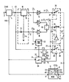
- the reference numeral 1 denotes an input terminal and 2 denotes an output terminal of the picture signal processing circuit.
- the reference numeral 3 denotes an input terminal for supplying a video signal CVHS to be processed.
- the signal CVHS comprises a line and field-sequentially composed picture signal CS and a synchronizing signal VHS which comprises, for example line and field-synchronizing pulses, blanking pulses and equalizing pulses.
- the video signal CVHS may be fixed or not fixed in a television standard and upon display it may present a non-interlaced picture or a single or multiple interlaced picture.
- the frame period In the case of single interlacing there is a field period of, for example 20 s or 16.6833 s and a line period of 64 ⁇ s or 63.555 ⁇ s, respectively, the frame period being equal to the double field period.
- the frame period In the case of non-interlacing the frame period is identical to the field period and in the case of 20 ms a frame or field frequency of 50 Hz is associated therewith.
- the field frequency or field period may be chosen to be equal to 100 Hz or 10 ms, respectively, in the case of interlacing or non-interlacing.
- the specific composition of the video signal CVHS is further disregarded.
- the line and field-sequentially composed picture signal CS is assumed to be originating from a picture signal source forming part of a television system in its widest sense. Examples are broadcast television, X-ray or infrared television, television for monitoring purposes, for displaying computer data etc. In this case there may be a display with moving or stationary pictures. Furthermore the picture signal CS may be a luminance, chrominance or colour difference signal in the case of colour television or a picture signal in the case of monochrome television.
- the reference numeral 4 denotes a circuit which operates inter alia as a signal separating circuit for supplying the picture signal CS and the field and line-synchronizing signal VHS when the video signal CVHS is supplied. Furthermore the circuit 4 may comprise signal correction circuits such as a de-gamma correction circuit. If the signal CVHS is a digital signal, the circuit 4 may comprise a D/A converter when the signal processing circuit with the input terminal 1 and the output terminal 2 is operative on an analog basis. If this circuit operates on a digital basis and if an analog signal CVHS is presented, the circuit 4 will comprise an A/D converter.
- the Figure shows a picture display device MON denoted by the reference numeral 5, an input 6 of which is coupled to the circuit 4 for supplying the signal VHS. An input 7 is coupled to the output terminal 2 for supplying the processed picture signal which is denoted by CS′.
- the device 5 is shown with a display screen 8 in which two picture signals CS1 and CS2 are shown diagrammatically by way of example.
- the signal CS1 is shown with a small amplitude and it is displayed by means of an electron beam with a small beam spot e1 on the screen 8.
- the signal CS2 is shown with a larger amplitude and is associated with a larger electron beam spot e2.
- the electron beam e is generated by an electron gun (not shown) which is present in an electron display tube which forms part of the display device 5.
- the display screen 8 of the display tube is scanned by the electron beam e under the control of line and field deflection means such as, for example deflection coils.
- the diameter of the spot e1 or e2 is dependent on the instantaneous picture signal amplitude. In this case a larger amplitude is accompanied by a reduced picture resolution which is fixed by the spot size.
- the weaker picture signal CS1 has a higher picture resolution upon display than the stronger picture signal CS2. According to the invention the stronger picture signal CS2 will be displayed with an improved high-frequency picture resolution due to the formation of the picture signal CS′.
- the input terminal 1 is coupled to an input 9 of a filter circuit 10 which has a first output 11 and a second output 12.
- the input 9 is coupled via a capacitor 13 to the output 12 which is further coupled to ground via a resistor 14.
- the capacitor 13 and the resistor 14 combined constitute a high-pass filter (13, 14) in its simplest form.
- the filter circuit 10 also comprises a subtractor circuit 15 having a (+) input which is coupled to the input 9 and a (-) input which is coupled to the output 12.
- An output of the circuit 15 is coupled to the filter output 11.
- the circuit 15 operates as a low-pass filter (13, 14, 15).
- the embodiment shown means that the filter circuit 10 comprises complementary filters (13, 14) and (13, 14, 15).
- the picture signal CS is split into a low-frequency picture signal component CS L and a high-frequency picture signal component CS H , which are complementary.
- two separate low-pass and high-pass filters could be used which are complementary or not complementary. Overlapping filter characteristics or separated, non-contiguous filter characteristics may be present in this case. In practice complementary filter characteristics for the high-frequency resolution improvement appear to be preferred.
- the output 11 is coupled to an input of a first amplifier circuit 16 and a second amplifier circuit 17.
- the output 12 is coupled to an input of a third amplifier circuit 18.
- Outputs of the circuits 17 and 18 are coupled to (+) inputs of an adder circuit 19.
- the circuits 16, 17 and 18 are shown with adjustable gain factors denoted p, q and r, respectively.
- the factors p, q and r may be adjustable or dynamically adjustable, dependent on the picture signal contents. Fixed factors p, q and r determined by calculation could also be present. The adjustability is a possible option.
- the reference numeral 20 in the Figure denotes a time-division multiplex circuit.
- a first input 21 and a second input 22 are coupled to an output of the circuits 16 and 19, respectively, which supply a signal p.CS L and q.CS L + r.CS H , respectively.
- the circuit 20 has a switching input 23 for applying a switching signal VS and an output 24 for supplying the processed picture signal CS′
- the circuit is shown with a first switch 25 and a second switch 26, the switching signal VS controlling the switch 25 directly and the switch 26 via an inverter circuit 27. Consequently, in the open or closed state of the switch 25, the switch 26 will be closed or open, respectively.
- the switches 25 and 26 are shown as mechanical switches, but in practice they will be electronic switches.
- the processed picture signal CS′ which is supplied from the output terminal 2 via the output 24 of the circuit 20 has undergone a time-division multiplex signal processing.
- the signal VS to be supplied by a switching signal generator 28 is applied to the switching input 23.
- a first output 29 of the generator 28 supplies the switching signal VS, while a short-circuit signal S is available at a second output 30.
- the synchronizing signal VHS is applied to a first input 31 of the generator 28.
- the result is the supply of the switching signal VS shown.
- Two field or frame periods TV are denoted by TV1 and TV2 at the signal VS.
- the signal VS shows a periodical switching signal of the double field or frame period 2TV.
- the short-circuit signal S is supplied by the generator 28 when the switching signal VS is absent, more specifically while applying a signal to a second input 32 of the generator 28, which signal originates from a circuit 33 for measuring modulation depth.
- the circuit 33 for measuring modulation depth has an input 34 which is coupled to the output 12 of the filter circuit 10 and to an output 35 to be coupled to the input 32 of the generator 28.
- the measurement of the modulation depth is illustrated by M and O.
- the generator 28 supplies the short-circuit signal 5 to be applied to a short-circuit switch 36.
- the switch 36 has an input 37 which is connected to the input terminal 1, while a short-circuit input 38 is coupled to the output 30.
- the switch 36 is shown with a switching member 39 which is controlled via the short-circuit input 38.
- An output 40 is connected to the output terminal 2.
- the block-schematic diagram of the Figure shows that, for example the picture signal component p.CS L during first periods TV1 and then the picture signal component q.CS L + r.CS H during second periods TV2 are periodically applied for display to the device 5 with a period 2TV which is equal to the double field or frame period TV.
- the picture signal CS2 shown this means that a picture signal component CS21 which is present under a broken line is displayed during the first periods TV1, while a component CS22 which is present above the broken line is displayed during the second periods TV2.
- the component CS21 is displayed with the electron beam spot e2, while the component CS22 is displayed with the spot e1. Consequently, the low-frequency picture information is displayed with the low picture resolution, while the combined high and low-frequency picture information is displayed with a higher picture resolution.
- the picture resolution improvement is based on the presupposition that the high-frequency picture signal component CS H does not have a maximum modulation depth of 100%. In practice, this presupposition holds true for substantially all picture signal sources, except for electronic test signal generators as a picture signal source. If the picture signal component CS H has a high modulation depth and if this component is displayed with the larger electron beam spot e2, the picture appears to have a poorer quality in practice.
- the short-circuit switch 36 is provided in the circuit according to the invention, because then the original picture resolution is the optimum possible picture resolution.
- the low-frequency component CS L is present as a pedestal for the high-frequency component CS H . This pedestal is required to ensure that the total signal CS22 is always positive.
- the spatial time-division multiplex display is effected with a period which is equal to the double field period TV.
- p + q and r are approximately equal to two.
- the picture signal CS is, for example a luminance signal, while associated chrominance or colour difference signals are directly applied in an unprocessed form to the display device 5.
- the display device 5 may comprise a projection display tube in which the picture on the screen 8 is projected on a projection screen via a system of lenses.
- the two picture signal components could each be applied to a separate projection display tube, while a picture combination is formed on the projection screen via the system of lenses.
- a high picture brightness and resolution is the result upon display.
Landscapes
- Engineering & Computer Science (AREA)
- Physics & Mathematics (AREA)
- General Physics & Mathematics (AREA)
- Theoretical Computer Science (AREA)
- Multimedia (AREA)
- Signal Processing (AREA)
- Television Systems (AREA)
- Picture Signal Circuits (AREA)
- Transforming Electric Information Into Light Information (AREA)
Applications Claiming Priority (2)
| Application Number | Priority Date | Filing Date | Title |
|---|---|---|---|
| NL8802426 | 1988-10-04 | ||
| NL8802426 | 1988-10-04 |
Publications (2)
| Publication Number | Publication Date |
|---|---|
| EP0367316A1 true EP0367316A1 (de) | 1990-05-09 |
| EP0367316B1 EP0367316B1 (de) | 1993-09-08 |
Family
ID=19852990
Family Applications (1)
| Application Number | Title | Priority Date | Filing Date |
|---|---|---|---|
| EP89202434A Expired - Lifetime EP0367316B1 (de) | 1988-10-04 | 1989-09-28 | Bildsignalbearbeitungsschaltung zur Steigerung der HF-Bildauflösung bei Bildsignalwiedergabe |
Country Status (4)
| Country | Link |
|---|---|
| US (1) | US5103219A (de) |
| EP (1) | EP0367316B1 (de) |
| JP (1) | JPH02149071A (de) |
| DE (1) | DE68908999T2 (de) |
Families Citing this family (1)
| Publication number | Priority date | Publication date | Assignee | Title |
|---|---|---|---|---|
| JPH0944122A (ja) * | 1995-08-03 | 1997-02-14 | Sharp Corp | 液晶表示システム |
Citations (2)
| Publication number | Priority date | Publication date | Assignee | Title |
|---|---|---|---|---|
| US3980819A (en) * | 1974-11-01 | 1976-09-14 | Zenith Radio Corporation | Edge enhancement for television images |
| US4258298A (en) * | 1979-12-28 | 1981-03-24 | Sperry Corporation | Dynamic focus control and power supply for cathode ray tube displays |
Family Cites Families (5)
| Publication number | Priority date | Publication date | Assignee | Title |
|---|---|---|---|---|
| US4314245A (en) * | 1980-03-10 | 1982-02-02 | Wilbur Jr John R | Video compensation subcircuit |
| JPS57109479A (en) * | 1980-12-26 | 1982-07-07 | Sony Corp | Picture quality adjusting circuit |
| US4358788A (en) * | 1981-02-27 | 1982-11-09 | Rca Corporation | Legibility for alpha-mosaic characters |
| US4484188A (en) * | 1982-04-23 | 1984-11-20 | Texas Instruments Incorporated | Graphics video resolution improvement apparatus |
| US4573081A (en) * | 1983-08-26 | 1986-02-25 | Rca Corporation | Frequency selective video signal compression |
-
1989
- 1989-09-28 EP EP89202434A patent/EP0367316B1/de not_active Expired - Lifetime
- 1989-09-28 DE DE89202434T patent/DE68908999T2/de not_active Expired - Fee Related
- 1989-09-29 US US07/414,088 patent/US5103219A/en not_active Expired - Fee Related
- 1989-10-02 JP JP1257631A patent/JPH02149071A/ja active Pending
Patent Citations (2)
| Publication number | Priority date | Publication date | Assignee | Title |
|---|---|---|---|---|
| US3980819A (en) * | 1974-11-01 | 1976-09-14 | Zenith Radio Corporation | Edge enhancement for television images |
| US4258298A (en) * | 1979-12-28 | 1981-03-24 | Sperry Corporation | Dynamic focus control and power supply for cathode ray tube displays |
Also Published As
| Publication number | Publication date |
|---|---|
| US5103219A (en) | 1992-04-07 |
| DE68908999D1 (de) | 1993-10-14 |
| DE68908999T2 (de) | 1994-03-17 |
| EP0367316B1 (de) | 1993-09-08 |
| JPH02149071A (ja) | 1990-06-07 |
Similar Documents
| Publication | Publication Date | Title |
|---|---|---|
| US4670784A (en) | Methods for coping with non-uniform phosphor aging in dual mode television receivers | |
| US5146331A (en) | Apparatus for adjusting picture quality of high definition television signals of either standard or wide aspect ratios displayed on a wide aspect ratio display | |
| US4556906A (en) | Kinescope blanking scheme for wide-aspect ratio television | |
| US4524379A (en) | Double-scanning non-interlace television receiver with vertical aperture correction circuit | |
| JPH0614712B2 (ja) | コンパチブル・ワイドアスペクト比テレビジョン信号発生装置 | |
| KR920004563B1 (ko) | 영상 재생 장치에 의해 유입된 전류를 변화시키는 장치 | |
| US4709267A (en) | Synchronizing circuit with improved interlace arrangement | |
| US4774580A (en) | Video signal control apparatus | |
| EP0367316B1 (de) | Bildsignalbearbeitungsschaltung zur Steigerung der HF-Bildauflösung bei Bildsignalwiedergabe | |
| US4092666A (en) | Monochrome presentation of demodulated color signals | |
| JPH0722400B2 (ja) | 運動補償方式 | |
| US5166780A (en) | Apparatus for showing a digitized NTSC-encoded video | |
| JPH0646784B2 (ja) | マルチ走査形テレビジヨン受像機 | |
| US3637921A (en) | Luminance amplifier with black level stabilization control | |
| KR0148141B1 (ko) | 블랭킹레벨조정방법 및 그 장치 | |
| JP3363624B2 (ja) | 黒伸長回路 | |
| KR960007647B1 (ko) | Secam방식 영상처리시스템에 있어서 문자발생장치 | |
| KR200159621Y1 (ko) | 와이드텔레비젼의 흑레벨보상장치 | |
| KR100265037B1 (ko) | 텔레비젼의표준신호레벨검출라인발생방법및그장치 | |
| JPH06269014A (ja) | 画像補正装置 | |
| JP2917682B2 (ja) | 映像信号処理回路 | |
| JPS63199594A (ja) | 電子画像エンコ−ダ | |
| JPH03273787A (ja) | カラー撮像装置 | |
| JPH0385066A (ja) | テレビジョン受像機 | |
| JPH02215293A (ja) | 高品位テレビジョン表示装置 |
Legal Events
| Date | Code | Title | Description |
|---|---|---|---|
| PUAI | Public reference made under article 153(3) epc to a published international application that has entered the european phase |
Free format text: ORIGINAL CODE: 0009012 |
|
| AK | Designated contracting states |
Kind code of ref document: A1 Designated state(s): DE FR GB NL |
|
| 17P | Request for examination filed |
Effective date: 19901107 |
|
| 17Q | First examination report despatched |
Effective date: 19921027 |
|
| GRAA | (expected) grant |
Free format text: ORIGINAL CODE: 0009210 |
|
| AK | Designated contracting states |
Kind code of ref document: B1 Designated state(s): DE FR GB NL |
|
| PG25 | Lapsed in a contracting state [announced via postgrant information from national office to epo] |
Ref country code: NL Effective date: 19930908 Ref country code: FR Effective date: 19930908 |
|
| REF | Corresponds to: |
Ref document number: 68908999 Country of ref document: DE Date of ref document: 19931014 |
|
| PG25 | Lapsed in a contracting state [announced via postgrant information from national office to epo] |
Ref country code: GB Effective date: 19931208 |
|
| EN | Fr: translation not filed | ||
| NLV1 | Nl: lapsed or annulled due to failure to fulfill the requirements of art. 29p and 29m of the patents act | ||
| PLBE | No opposition filed within time limit |
Free format text: ORIGINAL CODE: 0009261 |
|
| STAA | Information on the status of an ep patent application or granted ep patent |
Free format text: STATUS: NO OPPOSITION FILED WITHIN TIME LIMIT |
|
| GBPC | Gb: european patent ceased through non-payment of renewal fee |
Effective date: 19931208 |
|
| 26N | No opposition filed | ||
| PGFP | Annual fee paid to national office [announced via postgrant information from national office to epo] |
Ref country code: DE Payment date: 19981123 Year of fee payment: 10 |
|
| PG25 | Lapsed in a contracting state [announced via postgrant information from national office to epo] |
Ref country code: DE Free format text: LAPSE BECAUSE OF NON-PAYMENT OF DUE FEES Effective date: 20000701 |