EP0367411A2 - Dispositifs semi-conducteurs à hétérojonction et méthodes de fabrication correspondantes - Google Patents
Dispositifs semi-conducteurs à hétérojonction et méthodes de fabrication correspondantes Download PDFInfo
- Publication number
- EP0367411A2 EP0367411A2 EP89310184A EP89310184A EP0367411A2 EP 0367411 A2 EP0367411 A2 EP 0367411A2 EP 89310184 A EP89310184 A EP 89310184A EP 89310184 A EP89310184 A EP 89310184A EP 0367411 A2 EP0367411 A2 EP 0367411A2
- Authority
- EP
- European Patent Office
- Prior art keywords
- group iii
- compound semiconductor
- layer
- semiconductor layer
- semiconductor device
- Prior art date
- Legal status (The legal status is an assumption and is not a legal conclusion. Google has not performed a legal analysis and makes no representation as to the accuracy of the status listed.)
- Ceased
Links
Images


Classifications
-
- H—ELECTRICITY
- H10—SEMICONDUCTOR DEVICES; ELECTRIC SOLID-STATE DEVICES NOT OTHERWISE PROVIDED FOR
- H10D—INORGANIC ELECTRIC SEMICONDUCTOR DEVICES
- H10D30/00—Field-effect transistors [FET]
- H10D30/01—Manufacture or treatment
- H10D30/015—Manufacture or treatment of FETs having heterojunction interface channels or heterojunction gate electrodes, e.g. HEMT
-
- H—ELECTRICITY
- H10—SEMICONDUCTOR DEVICES; ELECTRIC SOLID-STATE DEVICES NOT OTHERWISE PROVIDED FOR
- H10D—INORGANIC ELECTRIC SEMICONDUCTOR DEVICES
- H10D30/00—Field-effect transistors [FET]
- H10D30/40—FETs having zero-dimensional [0D], one-dimensional [1D] or two-dimensional [2D] charge carrier gas channels
- H10D30/47—FETs having zero-dimensional [0D], one-dimensional [1D] or two-dimensional [2D] charge carrier gas channels having two-dimensional [2D] charge carrier gas channels, e.g. nanoribbon FETs or high electron mobility transistors [HEMT]
- H10D30/471—High electron mobility transistors [HEMT] or high hole mobility transistors [HHMT]
- H10D30/473—High electron mobility transistors [HEMT] or high hole mobility transistors [HHMT] having confinement of carriers by multiple heterojunctions, e.g. quantum well HEMT
- H10D30/4732—High electron mobility transistors [HEMT] or high hole mobility transistors [HHMT] having confinement of carriers by multiple heterojunctions, e.g. quantum well HEMT using Group III-V semiconductor material
-
- H—ELECTRICITY
- H10—SEMICONDUCTOR DEVICES; ELECTRIC SOLID-STATE DEVICES NOT OTHERWISE PROVIDED FOR
- H10D—INORGANIC ELECTRIC SEMICONDUCTOR DEVICES
- H10D62/00—Semiconductor bodies, or regions thereof, of devices having potential barriers
- H10D62/80—Semiconductor bodies, or regions thereof, of devices having potential barriers characterised by the materials
- H10D62/82—Heterojunctions
- H10D62/824—Heterojunctions comprising only Group III-V materials heterojunctions, e.g. GaN/AlGaN heterojunctions
-
- H—ELECTRICITY
- H10—SEMICONDUCTOR DEVICES; ELECTRIC SOLID-STATE DEVICES NOT OTHERWISE PROVIDED FOR
- H10D—INORGANIC ELECTRIC SEMICONDUCTOR DEVICES
- H10D84/00—Integrated devices formed in or on semiconductor substrates that comprise only semiconducting layers, e.g. on Si wafers or on GaAs-on-Si wafers
- H10D84/01—Manufacture or treatment
- H10D84/02—Manufacture or treatment characterised by using material-based technologies
- H10D84/05—Manufacture or treatment characterised by using material-based technologies using Group III-V technology
-
- H—ELECTRICITY
- H10—SEMICONDUCTOR DEVICES; ELECTRIC SOLID-STATE DEVICES NOT OTHERWISE PROVIDED FOR
- H10P—GENERIC PROCESSES OR APPARATUS FOR THE MANUFACTURE OR TREATMENT OF DEVICES COVERED BY CLASS H10
- H10P50/00—Etching of wafers, substrates or parts of devices
- H10P50/20—Dry etching; Plasma etching; Reactive-ion etching
- H10P50/24—Dry etching; Plasma etching; Reactive-ion etching of semiconductor materials
- H10P50/246—Dry etching; Plasma etching; Reactive-ion etching of semiconductor materials of Group III-V materials
Definitions
- the present invention generally relates to semiconductor devices and production methods thereof, and more particularly to a semiconductor device which uses as a channel a two dimensional electron gas layer which is generated using an InAlAs/InGaAs system heterojunction and a production method thereof.
- HEMT high electron mobility transistor
- a HEMT which uses an InAlAs/InGaAs system heterojunction has the following advantageous features. That is, the electron saturation velocity of an InGaAs channel layer is large and the electron mobility is high, and an n-type InAlAs electron supply layer can be doped to a high density and there is little deep impurity level. Furthermore, because the band discontinuity between InAlAs and InGaAs is large compared to the AlGaAs/GaAs system, it is possible to obtain a high electron gas density n s in the two dimensional electron gas layer.
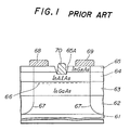
- FIG.1 is a cross sectional view generally showing an essential part of a conventional HEMT using an n-type InAlAs/InGaAs system heterojunction.
- the HEMT comprises a semiinsulating InP substrate 61, a non-doped InAlAs buffer layer 62, a non-doped InGaAs channel layer 63, an n-type InAlAs electron supply layer 64, an n-type InGaAs cap layer 65, a gate recess 65A, a two dimensional electron gas layer 66, a device isolation region 67 which is formed by implanting oxygen ions, a source electrode 68, a drain electrode 69, and a gate electrode 70.
- the source electrode 68 and the drain electrode 69 of this HEMT are formed on the n-type InGaAs cap layer 65 so as to obtain satisfactory ohmic contacts.
- the gate electrode 70 which requires a Schottky contact is formed on the n-type InAlAs electron supply layer 64 which is selectively exposed at the gate recess 65A by forming the gate recess 65A in the n-type InGaAs cap layer 65 (that is, the ohmic contact layer).
- the threshold voltage is controlled by the formation of the gate recess 65A.
- an appropriate selective dry etching technique for the InAlAs/InGaAs system When a dry etching technique with a low selective etching characteristic is used to form the gate recess 65A, it is impossible to uniformly etch a large area. Furthermore, such a dry etching damages the n-type InAlAs electron supply layer 64. As a result, the threshold voltages of the HEMTs cannot be made uniform and the device characteristics deteriorate, thereby making the HEMT unsuited for production in the form of an integrated circuit.
- the gate recess 65A is presently formed by use of a wet chemical etching which has a low selective etching characteristic. Although no etching damage is introduced on the n-type InAlAs electron supply layer 64 in this case, it is extremely difficult to obtain uniform device characteristics. In addition, the possibility of the short channel effect increases.
- Another and more specific object of the present invention is to provide a semiconductor device comprising a first group III-V compound semiconductor layer including indium (In), a second group III-V compound semiconductor layer formed on the first group III-V compound semiconductor layer and including no indium (In), and at least a recess formed in the second group III-V compound semiconductor layer, where the first group III-V compound semiconductor layer is exposed within the recess.
- a semiconductor device of the present invention it is possible to form the recess which accurately stops at the surface of the first group III-V compound semiconductor layer.
- Still another object of the present invention is to provide a semiconductor device comprising a semiinsulating substrate, a buffer layer formed on the semiinsulating substrate, a channel layer formed on the buffer layer, a carrier supply layer formed on the channel layer and made of a group III-V compound semiconductor including indium (In), a two dimensional electron gas layer formed in the channel layer in a vicinity of an interface between the channel layer and the carrier supply layer, a first group III-V compound semiconductor layer formed on the carrier supply layer and including no indium (In), a second group III-V compound semiconductor layer formed on the first group III-V compound semiconductor layer and including indium (In), a first gate recess formed in the second and first group III-V compound semiconductor layers, where the carrier supply layer is exposed within the first gate recess, and a first gate electrode formed on the carrier supply layer within the first gate recess.
- the semiconductor device of the present invention it is possible to produce transistors having uniform characteristics and reduced short channel effect. Hence, it is possible to integrate high-speed transistors such as HEMTs
- a further object of the present invention is to provide a method of producing a semiconductor device comprising the steps of forming a second group III-V compound semiconductor layer on a first group III-V compound semiconductor layer, where the first group III-V compound semiconductor layer includes indium (In) and the second compound semiconductor layer includes no indium (In), forming a third group III-V compound semiconductor layer on the second group III-V compound semiconductor layer, where the third group III-V compound semiconductor layer includes indium (In), and forming a recess in the third and second group III-V compound semiconductor layers so as to expose the first group III-V compound semiconductor layer within the recess, where the step of forming the recess uses a dry etching to remove the second group III-V compound semiconductor layer.
- the method of the present invention it is possible to accurately form uniform recesses without damaging the surface of the first group III-V compound semiconductor layer.
- Another object of the present invention is to provide a method of producing a semiconductor device comprising the steps of forming a buffer layer on a semiinsulating substrate, forming a channel layer on the buffer layer, forming a carrier supply layer on the channel layer, where the carrier supply layer is made of a group III-V compound semiconductor including indium and a two dimensional electron gas layer is formed in the channel layer in a vicinity of an interface between the channel layer and the carrier supply layer, forming a first group III-V compound semiconductor layer on the carrier supply layer, where the first group III-V compound semiconductor layer includes no indium (In), forming a second group III-V compound semiconductor layer on the first group III-V compound semiconductor layer, where the second group III-V compound semiconductor layer includes indium (In), forming a first gate recess in the second and first group III-V compound semiconductor layers so as to expose the carrier supply layer within the first gate recess, where the step of forming the first gate recess uses a dry etching to remove the first group III-V compound semiconductor layer, and
- FIGS.2A and 2B show essential production steps of the semiconductor device.
- a non-doped InAlAs buffer layer 2 a non-doped InGaAs channel layer 3, an n-type InAlAs electron supply layer 4, a non-doped GaAs layer 5 for recess etching, and an n-type InGaAs layer 6 for recess etching are successively formed on a semiinsulating InP substrate 1.
- a two dimensional electron gas layer 7 is formed when the n-type InAlAs electron supply layer 4 is formed on the non-doped InGaAs channel layer 3.
- a device isolation region 8 is formed by implanting oxygen ions.
- a source electrode 9 and a drain electrode 10 are formed on the n-type InGaAs layer 6.
- a gate recess 6A is formed in a prearranged portion of the n-type InGaAs layer 6 by a wet chemical etching. Thereafter, the gate recess 6A is made deeper by etching the non-doped GaAs layer 5 by a dry etching. When a chlorine system gas is used as the etching gas of this dry etching, it is possible to automatically stop the etching at the surface of the n-type InAlAs electron supply layer 4. An etching rate of InAlAs versus GaAs is approximately 1:200.
- a gate electrode 11 is formed on the n-type InAlAs electron supply layer 4 which is exposed within the gate recess 6A.
- a portion of the layer which is provided for the recess etching is made of GaAs.
- the non-doped GaAs layer 5 does not make a lattice matching with the n-type InAlAs electron supply layer 4 which is provided immediately thereunder, but no problems are generated when the non-doped GaAs layer 5 is made extremely thin so that no dislocation occurs.
- the n-type InGaAs layer 6 which is formed on the non-doped GaAs layer 5 constitutes another portion of the layer which is provided for the recess etching may be replaced by an n-type InAlAs layer or an n-type AlGaAs layer.
- a channel layer made of InGaAs (for example, the non-doped InGaAs channel layer 3) and a carrier supply layer made of InAlAs (for example, the n-type InAlAs electron supply layer 4) and a layer for recess etching made of GaAs (for example, the non-doped GaAs layer 5) are successively formed on a substrate (for example, the semiinsulating InP substrate 1).
- a gate recess is formed by etching the GaAs layer for recess etching by a dry etching (for example, a dry etching using an etching gas such as CCl2F2).
- the gate recesses which are formed become uniform within the wafer surface, and it is possible to produce with a satisfactory reproducibility a semiconductor device which comprises transistors with uniform device characteristics.
- the effects of the present invention is particularly notable when producing an integrated circuit of high-speed transistors such as HEMTs and producing enhancement/depletion type HEMTs.
- the semiconductor device is a HEMT.
- the buffer layer 2, the channel layer 3, the InAlAs electron supply layer 4, the layer 5 for recess etching, and the layer 6 for recess etching are successively formed on the semiinsulating InP substrate 1 by a molecular beam epitaxy (MBE).
- MBE molecular beam epitaxy
- the two dimensional electron gas layer 7 is formed when the electron supply layer 4 is formed on the channel layer 3.
- MOCVD metalorganic chemical vapor deposition
- each of the layers 2 through 6 are as follows.
- Electron Supply Layer 4
- a photoresist layer (not shown) is formed on the layer 6 in FIG.2B.
- This photoresist layer has an opening at a portion where the device isolation region is to be formed.
- oxygen ions are implanted through the opening in the photoresist layer so as to form the device isolation region 8.
- the ion implantation is carried out in two stages, where the first stage is carried out with a dosage of 1 x 1013 cm ⁇ 2 and an acceleration energy of 110 keV and the second stage is carried out with a dosage of 5 x 1012 cm ⁇ 2 and an acceleration energy of 50 keV. It if of course possible to employ a mesa isolation which is formed by the mesa etching.
- a photoresist layer (not shown) is formed on the layer 6 in FIG.2B.
- This photoresist layer has an opening at a portion where the ohmic contact electrode is to be formed.
- the magnetron sputtering By applying the magnetron sputtering, a AuGe/Au layer is formed.
- the thickness of the AuGe/Au layer is 1000 ⁇ /2000 ⁇ . It is of course possible to employ the evaporation instead of the magnetron sputtering.
- the photoresist layer which is formed in the Step 4) is removed so as to pattern the AuGe/Au layer by the lift-off method and form the source electrode 9 and the drain electrode 10.
- a photoresist process of the normal photolithography technique and a wet chemical etching are used to selectively etch the n-type InGaAs layer 6 and form the gate recess 6A.
- a selective dry etching using a chlorine system gas such as CCl2F2 as the etching gas is carried out to selectively etch the non-doped GaAs layer 5 and make the gate recess 6A deeper. This dry etching automatically stops at the surface of the n-type InAlAs electron supply layer 4.
- a mask constituted by the photoresist layer which is used to form the gate recess 6A is saved and an Al layer is formed by use of a magnetron sputtering or an evaporation.
- the mask is removed so as to pattern the Al layer by the lift-off method and form the gate electrode 11.
- the gate recess 6A is uniformly formed within the wafer surface and there is no damage to the n-type InAlAs electron supply layer 4 because the gate recess 6A is finally formed by the selective dry etching which automatically stops at the surface of the n-type InAlAs electron supply layer 4.
- the semiconductor device is an enhancement/depletion type HEMT.
- a MBE or MOCVD is used to form a buffer layer 22, a channel layer 23, an electron supply layer 24, and layers 25, 26, 27, 29 and 30 for recess etching are successively formed on a semiinsulating InP substrate 21.
- a two dimensional electron gas layer 31 is formed when the electron supply layer 24 is formed on the channel layer 23.
- each of the layers 22 through 27, 29 and 30 are as follows.
- Electron Supply Layer 24
- a photoresist layer (not shown) is formed on the layer 30 in FIG.3B.
- This photoresist layer has an opening at a portion where the device isolation region is to be formed.
- oxygen ions are implanted through the opening in the photoresist layer so as to form a device isolation region 28.
- the ion implantation is carried out in two stages, where the first stage is carried out with a dosage of 1 x 1013 cm ⁇ 2 and an acceleration energy of 110 keV and the second stage is carried out with a dosage of 5 x 1012 cm ⁇ 2 and an acceleration energy of 50 keV. It if of course possible to employ a mesa isolation which is formed by the mesa etching.
- a photoresist layer (not shown) is formed on the layer 30 in FIG.3B.
- This photoresist layer has an opening at a portion where the ohmic contact electrode is to be formed.
- a AuGe/Au layer is formed.
- the thickness of the AuGe/Au layer is 1000 ⁇ /2000 ⁇ .
- the photoresist layer which is formed in the Step 4) is removed so as to pattern the AuGe/Au layer by the lift-off method and form ohmic contact electrodes 32.
- the ohmic contact electrodes 32 from the left to right respectively are the source electrode, the drain/source electrode and the drain electrode.
- E denotes an enhancement type transistor portion and D denotes a depletion type transistor portion.
- a photoresist process of the normal photolithography technique and a wet chemical etching are used to selectively etch the n+-type GaAs layer 30, the n-type InGaAs layer 29 and the n+-type GaAs layer 27 and form a gate recess 30A.
- the wet chemical etching uses as an etchant a dilute mixture including fluoric acid and hydrogen peroxide.
- a mask 33 which is constituted by a photoresist layer is formed on the layer 30 and the ohmic contact electrodes 32 in FIG.3C.
- This mask 30 has an opening at a portion where the gate recess 30A is to be formed and at a portion where a gate recess of the depletion type transistor portion is to be formed.
- a first selective dry etching using a chlorine system gas such as CCl2F2 as the etching gas is carried out to selectively etch the n+-type GaAs layer 27 of the enhancement type transistor portion E and selectively etch the n+-type GaAs layer 30 of the depletion type transistor portion D.
- This first dry etching automatically stops at the surface of the n-type InAlAs layer 26 of the enhancement type transistor portion E and the n-type InGaAs layer 29 of the depletion type transistor portion D.
- the gate recess 30A becomes deeper in the enhancement type transistor portion E while a gate recess 30B is newly formed in the depletion type transistor portion D.
- a wet chemical etching is used to etch and remove the n-type InAlAs layer 26 which is exposed within the gate recess 30A and the n-type InGaAs layer 29 which is exposed within the gate recess 30B.
- This wet chemical etching uses as an etchant a dilute mixture including fluoric acid and hydrogen peroxide.
- a second selective dry etching using a chlorine system gas such as CCl2F2 as the etching gas is carried out to selectively etch the GaAs layer 25 of the enhancement type transistor portion E and selectively etch the n+-type GaAs layer 27 of the depletion type transistor portion D.
- This second dry etching automatically stops at the surface of the n-type In 0.52 Al 0.48 As electron supply layer 24 of the enhancement type transistor portion E and the n-type InAlAs layer 26 of the depletion type transistor portion D.
- the gate recess 30A becomes deeper in the enhancement type transistor portion E while the gate recess 30B also becomes deeper in the depletion type transistor portion D.
- the mask 33 constituted by the photoresist layer is saved and an Al layer is formed by use of a magnetron sputtering or an evaporation as shown in FIG.3D.
- the mask 33 is removed so as to pattern the Al layer by the lift-off method and form gate electrodes 34 and 35.
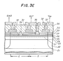
- a SiON interlayer insulator 36 is formed to a thickness of 7000 ⁇ , for example, by a known method as shown in FIG.3E. Further, known methods are used to form electrode contact windows and metal electrodes/interconnections made of TiPtAu, for example.
- GND denotes a ground terminal
- OUT denotes an output terminal
- V DD denotes a positive power source voltage terminal.
- the enhancement/depletion type HEMT which is produced by the above described steps of course has a uniform characteristic on the wafer surface.
- the semiconductor device is a enhancement/depletion type HEMT.
- a buffer layer 42, a channel layer 43, an electron supply layer 44, and layers 45 through 53 for recess etching are successively formed on a semiinsulating InP substrate 41.
- a two dimensional electron gas layer 54 is formed when the electron supply layer 44 is formed on the channel layer 43.
- each of the layers 42 through 53 are as follows.
- Electron Supply Layer 44
- the wafer having the layer structure shown in FIG.4A When the wafer having the layer structure shown in FIG.4A is used to produce the HEMT, it is possible to obtain a large voltage difference between the threshold voltage of the depletion type HEMT and the threshold voltage of the enhancement type HEMT.
- the total thickness of the GaAs layer 25 and the n-type InAlAs layer 26 is approximately 60 ⁇ so as not to generate the dislocation.
- the voltage difference between the threshold voltage of the enhancement type transistor portion E and the threshold voltage of the depletion type transistor portion D is only approximately 0.5 V.
- the GaAs/InAlAs layer for recess etching is doubled as shown in FIG.4A, that is, the GaAs layer 45, the n-type InAlAs layer 46, the GaAs layer 47, and the n-type InAlAs layer 48 are provided.
- the thickness of the GaAs/InAlAs layer for recess etching is 20 ⁇ /30 ⁇
- the total thickness of the GaAs/InAlAs layer for recess etching is doubled to 100 ⁇ when the GaAs/InAlAs layer for recess etching is doubled as shown in FIG.4A.
- the n-type InGaAs layers 50 and 52 which sandwich the GaAs layer 51 corresponds to the n-type InGaAs layer 29 shown in FIG.3A.
- the GaAs layer 45, the n-type InAlAs layer 46, the GaAs layer 47, and the n-type InAlAs layer 48 correspond to the GaAs layer 25 and the n-type InAlAs layer 26 shown in FIG.3A.
- steps similar to the Steps 2) through 6) of the second embodiment are carried out to form a device isolation region 101 and ohmic contact electrodes 102.
- a wet chemical etching is carried out similarly to the Step 7) of the second embodiment so as to selectively etch the layers 53, 52, 51 and 50 and a portion of the layer 49 in an enhancement type transistor portion E and form a gate recess 110A.
- a mask 103 is formed similarly to the Step 8) of the second embodiment, and a first selective dry etching is carried out similarly to the Step 9) of the second embodiment.
- the etching automatically stops at the n-type InAlAs layer 48 in the enhancement type transistor portion E and the gate recess 110A is made deeper.
- the etching automatically stops at the n-type InGaAs layer 52 in the depletion type transistor portion D and a gate recess 110B is formed.
- a wet chemical etching is carried out to remove the n-type InAlAs layer 48 exposed within the gate recess 110A and to remove the n-type InGaAs layer 52 exposed within the gate recess 110B, similarly to the Step 10) of the second embodiment.
- a second selective dry etching is carried out similarly to the Step 11) of the second embodiment.
- the etching automatically stops at the n-type InAlAs layer 46 in the enhancement type transistor portion E and the gate recess 110A is made deeper.
- the etching automatically stops at the n-type InGaAs layer 50 in the depletion type transistor portion D and the gate recess 110B is made deeper.
- a wet chemical etching is carried out to remove the n-type InAlAs layer 46 exposed within the gate recess 110A and to remove the n-type InGaAs layer 50 exposed within the gate recess 110B, similarly to the Step 10) of the second embodiment.
- a third selective dry etching is carried out similarly to the Step 11) of the second embodiment.
- the etching automatically stops at the n-type InAlAs layer 44 in the enhancement type transistor portion E and the gate recess 110A is made deeper.
- the etching automatically stops at the n-type InAlAs layer 48 in the depletion type transistor portion D and the gate recess 110B is made deeper.
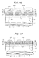
- steps similar to the Steps 12) and 13) of the second embodiment are carried out to form gate electrodes 104 and 105.
- Step 14 a step similar to the Step 14) of the second embodiment is carried out to form an interlayer insulator, electrode contact windows, and metal electrodes/interconnections.
- a top portion of the semiconductor device becomes similar to that of the second embodiment shown in FIG.3E.
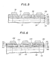
- FIG.5 shows an essential part of the modification of the second embodiment shown in FIG.3D.
- those parts which are the same as those corresponding parts in FIG.3D are designated by the same reference numerals, and a description thereof will be omitted.
- a InGaAs layer 130 is formed on the n+-type GaAs layer 30, so as to reduce the contact resistance at the electrodes 32.
- the InGaAs layer 130 has a thickness of 100 ⁇ and the impurity density of Si is 1 x 1019 cm ⁇ 3.
- FIG.6 shows an essential part of the modification of the third embodiment shown in FIG.4F.
- those parts which are the same as those corresponding parts in FIG.4F are designated by the same reference numerals, and a description thereof will be omitted.
- the InGaAs layer 130 is formed on the n+-type GaAs layer 53.
- the semiinsulating substrate is made of InP.
- GaAs, Si or the like for the substrate.
- the materials used for the channel layer and the electron supply layer are not limited to those described above, and other materials such as In 0.63 Ga 0.37 As and In 0.48 Al 0.52 As may be used for these layers.
- the dry etching using the chlorine system gas may be substituted by a dry etching using other gases including chlorine, fluoride and halogen as the etching gas.
Landscapes
- Junction Field-Effect Transistors (AREA)
- Recrystallisation Techniques (AREA)
Applications Claiming Priority (2)
| Application Number | Priority Date | Filing Date | Title |
|---|---|---|---|
| JP254971/88 | 1988-10-12 | ||
| JP63254971A JP2630446B2 (ja) | 1988-10-12 | 1988-10-12 | 半導体装置及びその製造方法 |
Publications (2)
| Publication Number | Publication Date |
|---|---|
| EP0367411A2 true EP0367411A2 (fr) | 1990-05-09 |
| EP0367411A3 EP0367411A3 (fr) | 1990-08-08 |
Family
ID=17272412
Family Applications (1)
| Application Number | Title | Priority Date | Filing Date |
|---|---|---|---|
| EP89310184A Ceased EP0367411A3 (fr) | 1988-10-12 | 1989-10-05 | Dispositifs semi-conducteurs à hétérojonction et méthodes de fabrication correspondantes |
Country Status (3)
| Country | Link |
|---|---|
| EP (1) | EP0367411A3 (fr) |
| JP (1) | JP2630446B2 (fr) |
| KR (1) | KR930001903B1 (fr) |
Cited By (7)
| Publication number | Priority date | Publication date | Assignee | Title |
|---|---|---|---|---|
| EP0448981A3 (en) * | 1990-03-06 | 1993-04-07 | Fujitsu Limited | High electron mobility transistor |
| EP0514079A3 (en) * | 1991-05-09 | 1993-07-21 | Raytheon Company | High electron mobility transistor and method of manufacture |
| EP0539688A3 (fr) * | 1991-10-29 | 1995-03-08 | Mitsubishi Electric Corp | |
| EP0855748A1 (fr) * | 1997-01-23 | 1998-07-29 | Nippon Telegraph And Telephone Corporation | Transistor à effet de champ à hétérojonction et méthode de fabrication correspondante |
| EP0932206A3 (fr) * | 1998-01-14 | 2000-01-26 | Matsushita Electric Industrial Co., Ltd. | Transistor à haute mobilité électronique |
| US6144048A (en) * | 1998-01-13 | 2000-11-07 | Nippon Telegraph And Telephone Corporation | Heterojunction field effect transistor and method of fabricating the same |
| US7573079B2 (en) | 2004-09-07 | 2009-08-11 | Fujitsu Limited | Field effect type semiconductor device |
Families Citing this family (1)
| Publication number | Priority date | Publication date | Assignee | Title |
|---|---|---|---|---|
| EP0452054B1 (fr) * | 1990-04-11 | 1995-07-12 | Hughes Aircraft Company | Structure HEMT à structure passivée |
Family Cites Families (1)
| Publication number | Priority date | Publication date | Assignee | Title |
|---|---|---|---|---|
| US4615102A (en) * | 1984-05-01 | 1986-10-07 | Fujitsu Limited | Method of producing enhancement mode and depletion mode FETs |
-
1988
- 1988-10-12 JP JP63254971A patent/JP2630446B2/ja not_active Expired - Lifetime
-
1989
- 1989-10-05 EP EP89310184A patent/EP0367411A3/fr not_active Ceased
- 1989-10-12 KR KR8914627A patent/KR930001903B1/ko not_active Expired - Fee Related
Cited By (9)
| Publication number | Priority date | Publication date | Assignee | Title |
|---|---|---|---|---|
| EP0448981A3 (en) * | 1990-03-06 | 1993-04-07 | Fujitsu Limited | High electron mobility transistor |
| EP0514079A3 (en) * | 1991-05-09 | 1993-07-21 | Raytheon Company | High electron mobility transistor and method of manufacture |
| EP0539688A3 (fr) * | 1991-10-29 | 1995-03-08 | Mitsubishi Electric Corp | |
| EP0855748A1 (fr) * | 1997-01-23 | 1998-07-29 | Nippon Telegraph And Telephone Corporation | Transistor à effet de champ à hétérojonction et méthode de fabrication correspondante |
| US6090649A (en) * | 1997-01-23 | 2000-07-18 | Nippon Telegraph And Telephone Corporation | Heterojunction field effect transistor and method of fabricating the same |
| US6144048A (en) * | 1998-01-13 | 2000-11-07 | Nippon Telegraph And Telephone Corporation | Heterojunction field effect transistor and method of fabricating the same |
| EP0932206A3 (fr) * | 1998-01-14 | 2000-01-26 | Matsushita Electric Industrial Co., Ltd. | Transistor à haute mobilité électronique |
| US6479896B1 (en) | 1998-01-14 | 2002-11-12 | Matsushita Electric Industrial Co., Ltd. | Semiconductor device having protective layer |
| US7573079B2 (en) | 2004-09-07 | 2009-08-11 | Fujitsu Limited | Field effect type semiconductor device |
Also Published As
| Publication number | Publication date |
|---|---|
| KR930001903B1 (en) | 1993-03-19 |
| JP2630446B2 (ja) | 1997-07-16 |
| JPH02102545A (ja) | 1990-04-16 |
| EP0367411A3 (fr) | 1990-08-08 |
Similar Documents
| Publication | Publication Date | Title |
|---|---|---|
| CA1214575A (fr) | Fabrication d'un dispositif semiconducteur en gaas | |
| US6797994B1 (en) | Double recessed transistor | |
| US6271547B1 (en) | Double recessed transistor with resistive layer | |
| US4615102A (en) | Method of producing enhancement mode and depletion mode FETs | |
| US5041393A (en) | Fabrication of GaAs integrated circuits | |
| JP3101457B2 (ja) | 半導体装置 | |
| US4751195A (en) | Method of manufacturing a heterojunction bipolar transistor | |
| JP3233207B2 (ja) | 電界効果トランジスタの製造方法 | |
| EP0194197B1 (fr) | Transistor bipolaire à hétérojonction et son procédé de fabrication | |
| US5610410A (en) | III-V compound semiconductor device with Schottky electrode of increased barrier height | |
| EP1131849B1 (fr) | Transistors pseudomorphiques a forte mobilite d'electrons | |
| EP0397148B1 (fr) | Dispositif à hétérostructure et procédé pour sa fabrication | |
| EP0367411A2 (fr) | Dispositifs semi-conducteurs à hétérojonction et méthodes de fabrication correspondantes | |
| JPH0324782B2 (fr) | ||
| US6417035B2 (en) | Method for manufacturing a field effect transistor | |
| JP2773700B2 (ja) | 化合物半導体装置およびその製造方法 | |
| JP3380139B2 (ja) | 高電子移動度トランジスタおよびその製造方法 | |
| US5943577A (en) | Method of making heterojunction bipolar structure having air and implanted isolations | |
| Fink et al. | AlInAs/GalnAs/AlInAs MODFETs fabricated on InP and on GaAs with metamorphic buffer-a comparison | |
| JP2787589B2 (ja) | 半導体装置 | |
| JPH09172163A (ja) | 半導体装置の製造方法 | |
| JP3102947B2 (ja) | ヘテロ接合型電界効果トランジスタの素子間分離方法 | |
| JP2668418B2 (ja) | 半導体装置 | |
| JP3534370B2 (ja) | 半導体装置の製造方法 | |
| JP2002270821A (ja) | 電界効果型半導体装置の製造方法 |
Legal Events
| Date | Code | Title | Description |
|---|---|---|---|
| PUAI | Public reference made under article 153(3) epc to a published international application that has entered the european phase |
Free format text: ORIGINAL CODE: 0009012 |
|
| AK | Designated contracting states |
Kind code of ref document: A2 Designated state(s): DE FR GB |
|
| PUAL | Search report despatched |
Free format text: ORIGINAL CODE: 0009013 |
|
| AK | Designated contracting states |
Kind code of ref document: A3 Designated state(s): DE FR GB |
|
| 17P | Request for examination filed |
Effective date: 19901011 |
|
| 17Q | First examination report despatched |
Effective date: 19920805 |
|
| STAA | Information on the status of an ep patent application or granted ep patent |
Free format text: STATUS: THE APPLICATION HAS BEEN REFUSED |
|
| 18R | Application refused |
Effective date: 19950629 |