EP0367708B1 - Structure et procédé pour fabriquer une cellule mémoire à transistors verticaux complémentaires - Google Patents
Structure et procédé pour fabriquer une cellule mémoire à transistors verticaux complémentaires Download PDFInfo
- Publication number
- EP0367708B1 EP0367708B1 EP89480157A EP89480157A EP0367708B1 EP 0367708 B1 EP0367708 B1 EP 0367708B1 EP 89480157 A EP89480157 A EP 89480157A EP 89480157 A EP89480157 A EP 89480157A EP 0367708 B1 EP0367708 B1 EP 0367708B1
- Authority
- EP
- European Patent Office
- Prior art keywords
- epitaxial layer
- vertical transistor
- region
- conductivity
- base
- Prior art date
- Legal status (The legal status is an assumption and is not a legal conclusion. Google has not performed a legal analysis and makes no representation as to the accuracy of the status listed.)
- Expired - Lifetime
Links
Images

Classifications
-
- H—ELECTRICITY
- H10—SEMICONDUCTOR DEVICES; ELECTRIC SOLID-STATE DEVICES NOT OTHERWISE PROVIDED FOR
- H10D—INORGANIC ELECTRIC SEMICONDUCTOR DEVICES
- H10D84/00—Integrated devices formed in or on semiconductor substrates that comprise only semiconducting layers, e.g. on Si wafers or on GaAs-on-Si wafers
- H10D84/01—Manufacture or treatment
-
- H—ELECTRICITY
- H10—SEMICONDUCTOR DEVICES; ELECTRIC SOLID-STATE DEVICES NOT OTHERWISE PROVIDED FOR
- H10B—ELECTRONIC MEMORY DEVICES
- H10B10/00—Static random access memory [SRAM] devices
- H10B10/10—SRAM devices comprising bipolar components
-
- H—ELECTRICITY
- H10—SEMICONDUCTOR DEVICES; ELECTRIC SOLID-STATE DEVICES NOT OTHERWISE PROVIDED FOR
- H10D—INORGANIC ELECTRIC SEMICONDUCTOR DEVICES
- H10D84/00—Integrated devices formed in or on semiconductor substrates that comprise only semiconducting layers, e.g. on Si wafers or on GaAs-on-Si wafers
- H10D84/01—Manufacture or treatment
- H10D84/02—Manufacture or treatment characterised by using material-based technologies
- H10D84/05—Manufacture or treatment characterised by using material-based technologies using Group III-V technology
-
- H—ELECTRICITY
- H10—SEMICONDUCTOR DEVICES; ELECTRIC SOLID-STATE DEVICES NOT OTHERWISE PROVIDED FOR
- H10D—INORGANIC ELECTRIC SEMICONDUCTOR DEVICES
- H10D84/00—Integrated devices formed in or on semiconductor substrates that comprise only semiconducting layers, e.g. on Si wafers or on GaAs-on-Si wafers
- H10D84/60—Integrated devices formed in or on semiconductor substrates that comprise only semiconducting layers, e.g. on Si wafers or on GaAs-on-Si wafers characterised by the integration of at least one component covered by groups H10D10/00 or H10D18/00, e.g. integration of BJTs
- H10D84/67—Complementary BJTs
- H10D84/673—Vertical complementary BJTs
-
- Y—GENERAL TAGGING OF NEW TECHNOLOGICAL DEVELOPMENTS; GENERAL TAGGING OF CROSS-SECTIONAL TECHNOLOGIES SPANNING OVER SEVERAL SECTIONS OF THE IPC; TECHNICAL SUBJECTS COVERED BY FORMER USPC CROSS-REFERENCE ART COLLECTIONS [XRACs] AND DIGESTS
- Y10—TECHNICAL SUBJECTS COVERED BY FORMER USPC
- Y10S—TECHNICAL SUBJECTS COVERED BY FORMER USPC CROSS-REFERENCE ART COLLECTIONS [XRACs] AND DIGESTS
- Y10S148/00—Metal treatment
- Y10S148/011—Bipolar transistors
-
- Y—GENERAL TAGGING OF NEW TECHNOLOGICAL DEVELOPMENTS; GENERAL TAGGING OF CROSS-SECTIONAL TECHNOLOGIES SPANNING OVER SEVERAL SECTIONS OF THE IPC; TECHNICAL SUBJECTS COVERED BY FORMER USPC CROSS-REFERENCE ART COLLECTIONS [XRACs] AND DIGESTS
- Y10—TECHNICAL SUBJECTS COVERED BY FORMER USPC
- Y10S—TECHNICAL SUBJECTS COVERED BY FORMER USPC CROSS-REFERENCE ART COLLECTIONS [XRACs] AND DIGESTS
- Y10S148/00—Metal treatment
- Y10S148/072—Heterojunctions
-
- Y—GENERAL TAGGING OF NEW TECHNOLOGICAL DEVELOPMENTS; GENERAL TAGGING OF CROSS-SECTIONAL TECHNOLOGIES SPANNING OVER SEVERAL SECTIONS OF THE IPC; TECHNICAL SUBJECTS COVERED BY FORMER USPC CROSS-REFERENCE ART COLLECTIONS [XRACs] AND DIGESTS
- Y10—TECHNICAL SUBJECTS COVERED BY FORMER USPC
- Y10S—TECHNICAL SUBJECTS COVERED BY FORMER USPC CROSS-REFERENCE ART COLLECTIONS [XRACs] AND DIGESTS
- Y10S148/00—Metal treatment
- Y10S148/087—I2L integrated injection logic
-
- Y—GENERAL TAGGING OF NEW TECHNOLOGICAL DEVELOPMENTS; GENERAL TAGGING OF CROSS-SECTIONAL TECHNOLOGIES SPANNING OVER SEVERAL SECTIONS OF THE IPC; TECHNICAL SUBJECTS COVERED BY FORMER USPC CROSS-REFERENCE ART COLLECTIONS [XRACs] AND DIGESTS
- Y10—TECHNICAL SUBJECTS COVERED BY FORMER USPC
- Y10S—TECHNICAL SUBJECTS COVERED BY FORMER USPC CROSS-REFERENCE ART COLLECTIONS [XRACs] AND DIGESTS
- Y10S148/00—Metal treatment
- Y10S148/109—Memory devices
Definitions
- This invention relates generally to monolithically integrated bipolar devices and process for making the same, and, more particularly, to a gallium arsenide (GaAs) bipolar static memory device and a process for making the same.
- GaAs gallium arsenide
- VLSI very large scale integration
- RAM random access memory
- ECL emitter-coupled logic
- CTS complementary transistor switch
- CTS Memory devices employing a vertical NPN transistor and a relatively large lateral PNP transistor in silicon technology are known.
- III-V compounds such as gallium arsenide (GaAs), with higher electron mobility, higher transconductance, and less delay associated with less charge storage, have been considered important for high performance applications.
- JP-A-6377146 describes an inverter circuit comprised of a multicollector vertical NPN transistor and a vertical PNP transistor connected to its base and operating as the current injector.
- Still another object of the present invention is to provide a method of fabricating compact CTS memory cells.
- a device structure wherein the base region of a vertical PNP transistor merges and shares the collector region of a vertical NPN transistor; the collector region of the vertical PNP transistor merges and share the same base region of the vertical NPN transistor; and the emitter of the vertical PNP transistor is at the top, and the emitter of vertical NPN transistor is at the bottom in relation to the position of the emitter of the vertical PNP transistor.
- FIG. 1 is a schematic diagram showing one complementary transistor switch (CTS) memory cell connected to its Word Line, Drain Line and Bit Lines in a memory array arrangement.
- CTS complementary transistor switch
- FIGS. 2A - C show cross-sectional views of a semiconductor substrate at various intermediate states in the process of fabricating a half side of the symmetrical CTS cell in accordance with the present invention.
- FIGS. 2D shows a cross-sectional view of a half side of the symmetrical CTS cell structure in accordance with the present invention.
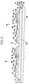
- FIG. 3 shows a cross-sectional view of a CTS cell structure comprising two identical half cell arrangements in accordance with the present invention.
- CTS cell 100 comprises cross-coupled bipolar NPN transistors 10 and 30, and complementary PNP bipolar transistors 20 and 40.
- the emitters of transistors 20 and 40 are connected to the Word Line 50 and the emitters of transistors 10 and 30 are connected to the Drain Line 60.
- the bases of transistors 20 and 40 are connected to the Left Bit Lines 70, and Right Bit Line 80, by way of Schottky barrier diodes (SBD) 72 and 82, respectively.
- SBDs 12 and 32 are connected to clamp the base and collector of transistors 10 and 30, respectively.
- CTS cell 100 permits the cell 100 to be divided into two half cells 98. Because of the symmetrical nature of the CTS cell 100, a detailed description of its half cell 98 and its fabrication, will allow a simplified explanation of the fabrication of the entire cell 100 in accordance with the present invention.
- the device structure 200 hereinafter also referred to as a half cell arrangment, in accordance with the invention for half cell 98 is illustrated in FIG. 2D.
- the vertical NPN transistor 10 of half cell 98 is constituted by N-type region 212B, P-type region 210A and N-type region 209 in undoped region 208B.
- the vertical PNP transistor 20 is constituted by P-type region 215, N-type region 212B and P-type layer 210A.
- the vertical NPN transistor 10 has its emitter 209 by way of the N+ region 206A at the bottom; and relative to the emitter 209 position of NPN transistor 10, the emitter 215 of the PNP transistor 20 is at the top.
- This feature of the half cell arrangement 200 improves greatly the wireability of the CTS cell 100 when connected in an array, especially in view of the common Word Line 50, the common Drain Line 60 as well as the orthogonal Left Bit Line 70 and Right Bit Line 80.
- the base region 210A of the vertical NPN transistor 10 is common with the collector region 210A of the vertical PNP transistor 20, and the collector region 212B of the vertical NPN transistor 10 is also in common with the base region 212B of the vertical PNP transistor 20.
- the fabrication of device structure 200 begins with a semi-insulating gallium arsenide substrate 202.
- An optional, though preferable, gallium arsenide buffer layer 204 could be formed on substrate 202.
- an N+ doped gallium arsenide layer 206 of about 200 - 400 nm (2000-4000 ⁇ ) thickness is formed over buffer layer 204.
- An undoped aluminum gallium arsenide layer 208 of about 100 nm (1000 ⁇ ) thickness is then grown over the N+ doped gallium arsenide layer 206.
- Layers 204, 206 and 208 are preferably formed successively in one metallorganic chemical vapor deposition (MOCVD) or molecular beam epitaxial (MBE) operation. Selected regions 209 in the aluminum gallium arsenide layer 208 could then be doped with N type dopants by utilizing a photoresist mask and by ion implantation.
- MOCVD metalorganic chemical vapor deposition
- MBE molecular beam
- a P-type gallium arsenide layer 210 of about 100 nm (1000 ⁇ ) thickness, an N-type gallium arsenide layer 212 of about 200 nm (2000 ⁇ ) thickness, and a P-type gallium arsenide layer 214 of about 200 nm (2000 ⁇ ) thickness are then successively formed using MOCVD or MBE.
- P-type gallium arsenide layer 214 is then etched away using well known and conventional lithographic and reactive ion etching (RIE) techniques leaving regions of P-type gallium arsenide 215 as illustrated in FIG 2C.
- RIE reactive ion etching
- portions of N-type layers 212, P-type layer 210 and undoped layer 208 are removed to expose layer 206.
- portions of N-type layer 212 are etched at region 218 to expose layer 210. Regions 212A and 212B remain contiguous and connected in the third dimension. The resulting structure is illustrated in FIG 2C.
- N-type dopants for example, silicon ions
- N+ regions 220 are formed on the surface of region 212B.
- substrate annealing to activate the implanted dopants.
- photoresist mask and ion implantation of non-conductive dopants for example, hydrogen ions, could be utilized to form isolation regions 222 surrounding device structure 200 and to isolate region 206A out of layer 206.
- Schottky barrier diodes (SBD) 12 and 72 could be formed on the N-type layer 212A via contacts 224A, 224B, respectively; and Ohmic contacts 224C, 224D could then be formed on the N+ regions 220 and the N+ region 206A respectively, preferably in a simultaneous fashion. Contacts 224B and 226A are connected via a conductor (not shown). Conventional lift-off techniques may be employed to remove any unwanted metallurgy. Furthermore, Ohmic contacts 226 to the P-type regions 210A and 215 could be made using conventional metallurgy; and lift-off techniques could be employed to remove any unwanted metal. The foregoing processing steps in accordance with the invention lead to the device structure 200 as illustrated in FIG. 2D.
- the processing could then be completed in a conventional fashion using a passivation layer; forming via holes in the passivation layer; forming an interconnection metallurgy; and then continuing on with higher level interconnection metallurgy.
- device structure 200 shows and describes a P-type gallium arsenide layer 214, on the top, it is clear that other alternatives are possible, for example, layer 214 could be aluminum gallium arsenide (AlGAs) with a P-doped region 215.
- AlGAs aluminum gallium arsenide
- FIG. 3 shows two half-cells 98 fabricated using two identical half cell arrangements 200, which are being isolated substantially from each other at etched region 216, to implement the CTS cell 100 in accordance with Applicant's invention. More particularly, the emitters of the NPN transistors in both half cell arrangements 200 are connected together by way of region 206A; the emitters of both the PNP transistors in both half cell arrangements 200 could be connected together; and both the NPN transistors are cross-coupled to form a CTS cell 100, which could be isolated from other CTS cell 100 by isolation region 222. More generally, many such CTS cells 100 could be integrated and interconnected in an array forming a static RAM integrated circuit device.
- the present invention teaches a device structure 200 featuring both a vertical NPN transistor 10 and a vertical complementary PNP transistor 20.
- the base region 212B of vertical PNP transistor 20 merges and shares the same collector region 212B of vertical transistor NPN 10.
- the collector region 210A of vertical PNP transistor 20 merges and shares the same base region 210A of vertical NPN transistor 10.
- the emitter of vertical PNP transistor 20 is at the top, and the emitter of vertical NPN transistor 10 is at the bottom in relation to the position of the emitter of vertical PNP transistor 20.
- This structural arrangement further improves the compactness and performance of the CTS cell 100. Even more importantly, this arrangement also improves the wireability of a memory array comprising many CTS cell 100, especially in view of the parallel Word Line 50 and Drain Line 60, as well as the pair of parallel Left Bit Line 70 and Right Bit Line 80, both of which are orthogonal to both Word Line 50 and Drain Line 60. While the resulting very compact device structure 200 improves density, performance and wireability, Applicant's invention, in accordance with the above teachings, is achieved by a fairly simple yet novel fabrication process.
Landscapes
- Semiconductor Memories (AREA)
- Bipolar Integrated Circuits (AREA)
- Bipolar Transistors (AREA)
Claims (16)
- Dispositif à structure semi-conductrice (200) ayant des transistors bipolaires complémentaires verticaux (10, 20), comprenant:a) un substrat semi-isolant (202);b) une première couche épitaxique (206) d'un premier type de conductivité (N+) revêtant ledit substrat;c) une couche isolante (208) ayant une région dopée (209) dudit premier type de conductivité revêtant ladite première couche épitaxique;d) une deuxième couche épitaxique (210) d'un deuxième type de conductivité (P) revêtant ladite couche isolante;e) une troisième couche épitaxique (212) dudit premier type de conductivité revêtant ladite deuxième couche épitaxique;f) une quatrième couche épitaxique (215) dudit deuxième type de conductivité revêtant ladite troisième couche épitaxique;g) un premier transistor vertical comprenant:i) un émetteur dudit premier type de conductivité étant constitué de ladite région dopée (209) de ladite couche isolante;ii) une base dudit deuxième type de conductivité étant constituée d'une région (210A) de ladite deuxième couche épitaxique; etiii) un collecteur (212B) dudit premier type de conductivité étant constitué d'une région de ladite troisième couche épitaxique; eth) un deuxième transistor vertical complémentaire audit premier transistor vertical, comprenant:dans lequel ledit émetteur dudit premier transistor vertical est en bas, et ledit émetteur dudit deuxième transistor vertical complémentaire est en haut par rapport audit émetteur dudit premier transistor vertical, et dans lequel la région de base (212B) du deuxième transistor vertical (20) fusionne et partage la même région de collecteur (212B) avec le premier transistor vertical (10), et la région de collecteur (210A) du deuxième transistor vertical (20) fusionne et partage la même région de base (210A) avec le premier transistor vertical (10).i) un émetteur qui est constitué d'une région (215) de ladite quatrième couche épitaxique;ii) une base qui est constituée de ladite région (212B) de ladite troisième couche épitaxique et commune audit collecteur dudit premier transistor vertical;iii) un collecteur qui est constitué de ladite région (212B) de ladite deuxième couche épitaxique et commun à ladite base dudit premier transistor vertical;
- Dispositif semi-conducteur selon la revendication 1, comprenant en outre une première diode à barrière de Schottky (72) connectée à la base dudit deuxième transistor, et une deuxième diode à barrière de Schottky (12) verrouillant la base et le collecteur dudit premier transistor formant un premier agencement de demi-cellule.
- Dispositif semi-conducteur selon la revendication 2, comprenant en outre:
un troisième transistor vertical (30), un quatrième transistor vertical (40) complémentaire audit troisième transistor vertical, et une troisième diode à barrière de Schottky (82) connectée à la base dudit quatrième transistor, et une quatrième diode à barrière de Schottky (32) verrouillant la base et le collecteur dudit troisième transistor formant un deuxième agencement de demi-cellule sensiblement isolé;
le collecteur et la base dudit premier transistor dans ledit premier agencement de demi-cellule étant respectivement connectés à la base et au collecteur dudit troisième transistor dans ledit deuxième agencement de demi-cellule;
les émetteur desdits premier et troisième transistors étant connectés; et
les émetteurs desdits deuxième et quatrième transistors étant connectés, formant de ce fait une cellule de mémoire CTS. - Dispositif semi-conducteur selon la revendicateur 3, dans lequel ladite première couche épitaxique est du type de conductivité N, ayant une concentration de dopage plus élevée que ladite région dopée de ladite couche isolante, et ladite deuxième couche épitaxique est du type de conductivité P.
- Dispositif semi-conducteur selon la revendication 4, comprenant en outre une couche tampon située entre ledit substrat semi-isolant et ladite première couche épitaxique.
- Dispositif semi-conducteur selon la revendication 5, dans lequel ledit substrat semi-isolant est de l'arséniure de gallium.
- Dispositif semi-conducteur selon les revendications 2 ou 3, dans lequel ladite couche isolante est AlGaAs.
- Dispositif semi-conducteur selon les revendications 2 ou 3, dans lequel ladite couche isolante est GaAs.
- Dispositif semi-conducteur selon les revendications 2 ou 3, dans lequel ladite quatrième couche épitaxique est GaAs ayant un dopant dudit deuxième type de conductivité.
- Dispositif semi-conducteur selon les revendications 2 ou 3, dans lequel ladite quatrième couche épitaxique est AlGaAs ayant un dopant dudit deuxième type de conductivité.
- Procédé de fabrication d'un dispositif semi-conducteur ayant des transistors bipolaires complémentaires verticaux, comprenant les étapes de:a) fournir un substrat semi-isolant;b) former une première couche épitaxique d'un premier type de conductivité revêtant ledit substrat;c) former une couche isolante ayant une région dopée dudit premier type de conductivité revêtant ladite couche épitaxique;d) former une deuxième couche épitaxique d'un deuxième type de conductivité revêtant ladite couche isolante;e) former une troisième couche épitaxique dudit premier type de conductivité revêtant ladite deuxième couche épitaxique;f) former une quatrième couche épitaxique dudit deuxième type de conductivité revêtant ladite troisième couche épitaxique;g) former un premier transistor vertical:i) un émetteur dudit premier type de conductivité qui est constitué de ladite région dopée de ladite couche isolante;ii) une base dudit deuxième type de conductivité qui est constituée d'une région (210A) de ladite deuxième couche épitaxique;iii) un collecteur dudit premier type de conductivité qui est constitué d'une région de ladite troisième couche épitaxique; eth) former un deuxième transistor vertical:dans lequel ledit émetteur dudit premier transistor vertical est en bas, et ledit émetteur dudit deuxième transistor vertical complémentaire est en haut par rapport audit émetteur dudit premier transistor vertical.i) un émetteur qui est constitué d'une région de ladite quatrième couche épitaxique;ii) une base qui est constituée de ladite région de ladite troisième couche épitaxique et commune audit collecteur dudit premier transistor vertical;iii) un collecteur qui est constitué de ladite région de ladite deuxième couche épitaxique et commun à ladite base dudit premier transistor vertical;
- Procédé de fabrication d'un dispositif semi-conducteur selon la revendication 11, dans lequel ladite région dopée dans ladite couche isolante est formée en formant tout d'abord une couche non dopée et en formant ensuite ladite région dopée par implantation ionique d'un dopant dudit premier type de conductivité.
- Procédé de fabrication d'un dispositif semi-conducteur selon la revendication 12, dans lequel ladite couche non dopée est AlGaAs ou GaAs.
- Procédé de fabrication d'un dispositif semi-conducteur selon la revendication 11, dans lequel ladite quatrième couche épitaxique est GaAs ou AlGaAs ayant un dopant dudit deuxième type de conductivité.
- Procédé de fabrication d'un dispositif semi-conducteur selon la revendication 11, comprenant en outre l'étape de former une couche tampon située entre ledit substrat semi-isolant et ladite première couche épitaxique.
- Procédé de fabrication d'un dispositif semi-conducteur selon la revendication 11, comprenant en outre l'étape de former, dans ladite troisième couche épitaxique, une première diode à barrière de Schottky se connectant à la base dudit deuxième transistor vertical, et une deuxième diode à barrière de Schottky verrouillant la base et le collecteur dudit premier transistor vertical.
Applications Claiming Priority (2)
| Application Number | Priority Date | Filing Date | Title |
|---|---|---|---|
| US265062 | 1988-10-31 | ||
| US07/265,062 US4981807A (en) | 1988-10-31 | 1988-10-31 | Process for fabricating complementary vertical transistor memory cell |
Publications (2)
| Publication Number | Publication Date |
|---|---|
| EP0367708A1 EP0367708A1 (fr) | 1990-05-09 |
| EP0367708B1 true EP0367708B1 (fr) | 1995-08-09 |
Family
ID=23008797
Family Applications (1)
| Application Number | Title | Priority Date | Filing Date |
|---|---|---|---|
| EP89480157A Expired - Lifetime EP0367708B1 (fr) | 1988-10-31 | 1989-10-10 | Structure et procédé pour fabriquer une cellule mémoire à transistors verticaux complémentaires |
Country Status (6)
| Country | Link |
|---|---|
| US (1) | US4981807A (fr) |
| EP (1) | EP0367708B1 (fr) |
| JP (1) | JPH0650764B2 (fr) |
| BR (1) | BR8905540A (fr) |
| CA (1) | CA1291577C (fr) |
| DE (1) | DE68923759T2 (fr) |
Families Citing this family (10)
| Publication number | Priority date | Publication date | Assignee | Title |
|---|---|---|---|---|
| US5223449A (en) * | 1989-02-16 | 1993-06-29 | Morris Francis J | Method of making an integrated circuit composed of group III-V compound field effect and bipolar semiconductors |
| US5097312A (en) * | 1989-02-16 | 1992-03-17 | Texas Instruments Incorporated | Heterojunction bipolar transistor and integration of same with field effect device |
| JPH04261026A (ja) * | 1991-01-08 | 1992-09-17 | Mitsubishi Electric Corp | 半導体装置及びその製造方法 |
| US5213987A (en) * | 1991-03-28 | 1993-05-25 | Texas Instruments Incorporated | Method of integrating heterojunction bipolar transistors with PIN diodes |
| US5166083A (en) * | 1991-03-28 | 1992-11-24 | Texas Instruments Incorporated | Method of integrating heterojunction bipolar transistors with heterojunction FETs and PIN diodes |
| US5268315A (en) * | 1992-09-04 | 1993-12-07 | Tektronix, Inc. | Implant-free heterojunction bioplar transistor integrated circuit process |
| US5994727A (en) * | 1997-09-30 | 1999-11-30 | Samsung Electronics Co., Ltd. | High performance gaas field effect transistor structure |
| EP1408549B1 (fr) * | 2002-10-08 | 2007-03-07 | STMicroelectronics S.r.l. | Procédé de fabrication d'une matrice de cellules comprenant de transistors bipolaires du sélection et matrice de cellules associée |
| DE60217120T2 (de) * | 2002-10-08 | 2007-10-25 | Stmicroelectronics S.R.L., Agrate Brianza | Zellenanordnung mit einem darin enthaltenen Auswähl-Bipolartransistor sowie Verfahren zum Herstellen derselben |
| US9264027B1 (en) * | 2013-03-14 | 2016-02-16 | Integrated Device Technology, Inc. | Process compensated delay |
Family Cites Families (18)
| Publication number | Priority date | Publication date | Assignee | Title |
|---|---|---|---|---|
| JPS549279B2 (fr) * | 1972-07-12 | 1979-04-23 | ||
| US4122482A (en) * | 1973-02-02 | 1978-10-24 | U.S. Philips Corporation | Vertical complementary bipolar transistor device with epitaxial base zones |
| US4274891A (en) * | 1979-06-29 | 1981-06-23 | International Business Machines Corporation | Method of fabricating buried injector memory cell formed from vertical complementary bipolar transistor circuits utilizing mono-poly deposition |
| US4485552A (en) * | 1980-01-18 | 1984-12-04 | International Business Machines Corporation | Complementary transistor structure and method for manufacture |
| US4483726A (en) * | 1981-06-30 | 1984-11-20 | International Business Machines Corporation | Double self-aligned fabrication process for making a bipolar transistor structure having a small polysilicon-to-extrinsic base contact area |
| US4573064A (en) * | 1981-11-02 | 1986-02-25 | Texas Instruments Incorporated | GaAs/GaAlAs Heterojunction bipolar integrated circuit devices |
| US4482906A (en) * | 1982-06-30 | 1984-11-13 | International Business Machines Corporation | Gallium aluminum arsenide integrated circuit structure using germanium |
| US4593305A (en) * | 1983-05-17 | 1986-06-03 | Kabushiki Kaisha Toshiba | Heterostructure bipolar transistor |
| US4617724A (en) * | 1983-06-30 | 1986-10-21 | Fujitsu Limited | Process for fabricating heterojunction bipolar transistor with low base resistance |
| US4586071A (en) * | 1984-05-11 | 1986-04-29 | International Business Machines Corporation | Heterostructure bipolar transistor |
| JPS60253283A (ja) * | 1984-05-29 | 1985-12-13 | Toshiba Corp | 半導体発光素子 |
| US4649411A (en) * | 1984-12-17 | 1987-03-10 | Motorola, Inc. | Gallium arsenide bipolar ECL circuit structure |
| US4635087A (en) * | 1984-12-28 | 1987-01-06 | Motorola, Inc. | Monolithic bipolar SCR memory cell |
| JPS6249658A (ja) * | 1985-08-29 | 1987-03-04 | Matsushita Electric Ind Co Ltd | ヘテロ接合バイポ−ラトランジスタおよびその製造方法 |
| US4771013A (en) * | 1986-08-01 | 1988-09-13 | Texas Instruments Incorporated | Process of making a double heterojunction 3-D I2 L bipolar transistor with a Si/Ge superlattice |
| JPS63188969A (ja) * | 1987-01-30 | 1988-08-04 | Matsushita Electric Ind Co Ltd | バイポ−ラトランジスタの製造方法 |
| JP2587826B2 (ja) * | 1987-03-27 | 1997-03-05 | 日本電信電話株式会社 | バイポ−ラトランジスタとその製造方法 |
| US4807008A (en) * | 1987-09-14 | 1989-02-21 | Rockwell International Corporation | Static memory cell using a heterostructure complementary transistor switch |
-
1988
- 1988-10-31 US US07/265,062 patent/US4981807A/en not_active Expired - Fee Related
-
1989
- 1989-06-08 CA CA000601596A patent/CA1291577C/fr not_active Expired - Lifetime
- 1989-09-20 JP JP1242392A patent/JPH0650764B2/ja not_active Expired - Lifetime
- 1989-10-10 DE DE68923759T patent/DE68923759T2/de not_active Expired - Fee Related
- 1989-10-10 EP EP89480157A patent/EP0367708B1/fr not_active Expired - Lifetime
- 1989-10-30 BR BR898905540A patent/BR8905540A/pt not_active Application Discontinuation
Non-Patent Citations (1)
| Title |
|---|
| IBM Journal of Research and Development, vol. 25, no. 3, 1981, pages 126-134 * |
Also Published As
| Publication number | Publication date |
|---|---|
| DE68923759D1 (de) | 1995-09-14 |
| CA1291577C (fr) | 1991-10-29 |
| JPH02137362A (ja) | 1990-05-25 |
| EP0367708A1 (fr) | 1990-05-09 |
| US4981807A (en) | 1991-01-01 |
| BR8905540A (pt) | 1990-05-29 |
| JPH0650764B2 (ja) | 1994-06-29 |
| DE68923759T2 (de) | 1996-04-18 |
Similar Documents
| Publication | Publication Date | Title |
|---|---|---|
| US3962717A (en) | Oxide isolated integrated injection logic with selective guard ring | |
| US5077231A (en) | Method to integrate HBTs and FETs | |
| US4543595A (en) | Bipolar memory cell | |
| US4338622A (en) | Self-aligned semiconductor circuits and process therefor | |
| US4066473A (en) | Method of fabricating high-gain transistors | |
| US5163178A (en) | Semiconductor device having enhanced impurity concentration profile | |
| US4433470A (en) | Method for manufacturing semiconductor device utilizing selective etching and diffusion | |
| US4593457A (en) | Method for making gallium arsenide NPN transistor with self-aligned base enhancement to emitter region and metal contact | |
| US4418468A (en) | Process for fabricating a logic structure utilizing polycrystalline silicon Schottky diodes | |
| US3993513A (en) | Combined method for fabricating oxide-isolated vertical bipolar transistors and complementary oxide-isolated lateral bipolar transistors and the resulting structures | |
| US4751195A (en) | Method of manufacturing a heterojunction bipolar transistor | |
| EP0367708B1 (fr) | Structure et procédé pour fabriquer une cellule mémoire à transistors verticaux complémentaires | |
| US4254428A (en) | Self-aligned Schottky diode structure and method of fabrication | |
| CA1205574A (fr) | Cellules de memoire a implantation ionique pour memoire vive a grande densite | |
| US7968416B2 (en) | Integrated circuit arrangement with NPN and PNP bipolar transistors and corresponding production method | |
| KR950014277B1 (ko) | 헤테로 접합형 바이폴러트랜지스터 | |
| JP2706034B2 (ja) | トランジスタ及びその製造方法 | |
| US4516223A (en) | High density bipolar ROM having a lateral PN diode as a matrix element and method of fabrication | |
| JPS62211917A (ja) | P型領域に低抵抗オ−ム接点を形成する方法 | |
| US4889823A (en) | Bipolar transistor structure for very high speed circuits and method for the manufacture thereof | |
| US4807008A (en) | Static memory cell using a heterostructure complementary transistor switch | |
| US4947230A (en) | Base-coupled transistor logic | |
| US4956689A (en) | High speed gallium arsenide transistor and method | |
| JP2868083B2 (ja) | 半導体デバイスの製造方法 | |
| US4624863A (en) | Method of fabricating Schottky diodes and electrical interconnections in semiconductor structures |
Legal Events
| Date | Code | Title | Description |
|---|---|---|---|
| PUAI | Public reference made under article 153(3) epc to a published international application that has entered the european phase |
Free format text: ORIGINAL CODE: 0009012 |
|
| AK | Designated contracting states |
Kind code of ref document: A1 Designated state(s): CH DE ES FR GB IT LI NL SE |
|
| 17P | Request for examination filed |
Effective date: 19900820 |
|
| 17Q | First examination report despatched |
Effective date: 19921119 |
|
| GRAA | (expected) grant |
Free format text: ORIGINAL CODE: 0009210 |
|
| AK | Designated contracting states |
Kind code of ref document: B1 Designated state(s): CH DE ES FR GB IT LI NL SE |
|
| PG25 | Lapsed in a contracting state [announced via postgrant information from national office to epo] |
Ref country code: IT Free format text: LAPSE BECAUSE OF FAILURE TO SUBMIT A TRANSLATION OF THE DESCRIPTION OR TO PAY THE FEE WITHIN THE PRESCRIBED TIME-LIMIT;WARNING: LAPSES OF ITALIAN PATENTS WITH EFFECTIVE DATE BEFORE 2007 MAY HAVE OCCURRED AT ANY TIME BEFORE 2007. THE CORRECT EFFECTIVE DATE MAY BE DIFFERENT FROM THE ONE RECORDED. Effective date: 19950809 Ref country code: ES Free format text: THE PATENT HAS BEEN ANNULLED BY A DECISION OF A NATIONAL AUTHORITY Effective date: 19950809 Ref country code: NL Free format text: LAPSE BECAUSE OF NON-PAYMENT OF DUE FEES Effective date: 19950809 Ref country code: FR Free format text: THE PATENT HAS BEEN ANNULLED BY A DECISION OF A NATIONAL AUTHORITY Effective date: 19950809 |
|
| REF | Corresponds to: |
Ref document number: 68923759 Country of ref document: DE Date of ref document: 19950914 |
|
| PGFP | Annual fee paid to national office [announced via postgrant information from national office to epo] |
Ref country code: DE Payment date: 19951030 Year of fee payment: 7 |
|
| PGFP | Annual fee paid to national office [announced via postgrant information from national office to epo] |
Ref country code: CH Payment date: 19951031 Year of fee payment: 7 |
|
| PG25 | Lapsed in a contracting state [announced via postgrant information from national office to epo] |
Ref country code: SE Effective date: 19951109 Ref country code: GB Effective date: 19951109 |
|
| NLV1 | Nl: lapsed or annulled due to failure to fulfill the requirements of art. 29p and 29m of the patents act | ||
| EN | Fr: translation not filed | ||
| PLBE | No opposition filed within time limit |
Free format text: ORIGINAL CODE: 0009261 |
|
| STAA | Information on the status of an ep patent application or granted ep patent |
Free format text: STATUS: NO OPPOSITION FILED WITHIN TIME LIMIT |
|
| GBPC | Gb: european patent ceased through non-payment of renewal fee |
Effective date: 19951109 |
|
| 26N | No opposition filed | ||
| PG25 | Lapsed in a contracting state [announced via postgrant information from national office to epo] |
Ref country code: LI Free format text: LAPSE BECAUSE OF FAILURE TO SUBMIT A TRANSLATION OF THE DESCRIPTION OR TO PAY THE FEE WITHIN THE PRESCRIBED TIME-LIMIT Effective date: 19961031 Ref country code: CH Free format text: LAPSE BECAUSE OF FAILURE TO SUBMIT A TRANSLATION OF THE DESCRIPTION OR TO PAY THE FEE WITHIN THE PRESCRIBED TIME-LIMIT Effective date: 19961031 |
|
| PG25 | Lapsed in a contracting state [announced via postgrant information from national office to epo] |
Ref country code: DE Effective date: 19970701 |