EP0367710B1 - Diagnostika einer Leiterplatte mit einer Mehrzahl elektronischer Hybridbauelemente - Google Patents
Diagnostika einer Leiterplatte mit einer Mehrzahl elektronischer Hybridbauelemente Download PDFInfo
- Publication number
- EP0367710B1 EP0367710B1 EP89480167A EP89480167A EP0367710B1 EP 0367710 B1 EP0367710 B1 EP 0367710B1 EP 89480167 A EP89480167 A EP 89480167A EP 89480167 A EP89480167 A EP 89480167A EP 0367710 B1 EP0367710 B1 EP 0367710B1
- Authority
- EP
- European Patent Office
- Prior art keywords
- board
- input
- component
- pins
- circuit board
- Prior art date
- Legal status (The legal status is an assumption and is not a legal conclusion. Google has not performed a legal analysis and makes no representation as to the accuracy of the status listed.)
- Expired - Lifetime
Links
Images




Classifications
-
- G—PHYSICS
- G06—COMPUTING OR CALCULATING; COUNTING
- G06F—ELECTRIC DIGITAL DATA PROCESSING
- G06F11/00—Error detection; Error correction; Monitoring
- G06F11/22—Detection or location of defective computer hardware by testing during standby operation or during idle time, e.g. start-up testing
- G06F11/26—Functional testing
- G06F11/261—Functional testing by simulating additional hardware, e.g. fault simulation
-
- G—PHYSICS
- G01—MEASURING; TESTING
- G01R—MEASURING ELECTRIC VARIABLES; MEASURING MAGNETIC VARIABLES
- G01R31/00—Arrangements for testing electric properties; Arrangements for locating electric faults; Arrangements for electrical testing characterised by what is being tested not provided for elsewhere
- G01R31/28—Testing of electronic circuits, e.g. by signal tracer
- G01R31/317—Testing of digital circuits
- G01R31/3181—Functional testing
- G01R31/3185—Reconfiguring for testing, e.g. LSSD, partitioning
- G01R31/318533—Reconfiguring for testing, e.g. LSSD, partitioning using scanning techniques, e.g. LSSD, Boundary Scan, JTAG
- G01R31/318544—Scanning methods, algorithms and patterns
-
- G—PHYSICS
- G01—MEASURING; TESTING
- G01R—MEASURING ELECTRIC VARIABLES; MEASURING MAGNETIC VARIABLES
- G01R31/00—Arrangements for testing electric properties; Arrangements for locating electric faults; Arrangements for electrical testing characterised by what is being tested not provided for elsewhere
- G01R31/28—Testing of electronic circuits, e.g. by signal tracer
- G01R31/317—Testing of digital circuits
- G01R31/3181—Functional testing
- G01R31/3185—Reconfiguring for testing, e.g. LSSD, partitioning
- G01R31/318533—Reconfiguring for testing, e.g. LSSD, partitioning using scanning techniques, e.g. LSSD, Boundary Scan, JTAG
- G01R31/318566—Comparators; Diagnosing the device under test
-
- G—PHYSICS
- G06—COMPUTING OR CALCULATING; COUNTING
- G06F—ELECTRIC DIGITAL DATA PROCESSING
- G06F11/00—Error detection; Error correction; Monitoring
- G06F11/22—Detection or location of defective computer hardware by testing during standby operation or during idle time, e.g. start-up testing
- G06F11/26—Functional testing
- G06F11/273—Tester hardware, i.e. output processing circuits
- G06F11/2733—Test interface between tester and unit under test
Definitions
- This invention relates broadly to the field of diagnostics of a fully populated electronic package which typically has a plurality of integrated circuit chips, multi-chip modules, cards, etc..
- Unit-in-place diagnostics is one form of diagnostic which can be performed sequentially on each individual board component or jointly on a group of selected board components.
- the present invention has particular utility when these electronic components to be tested are a mixed combination of structured and unstructured designs.
- the testing of a board comprised of a plurality of electronic components of diverse nature and origin requires the testing of each component separately and then mounting each component on the board.
- the board is then tested as a single entity, applying to it a set of test vectors generated to detect a substantial percentage of possible failures within the board.
- This technique is referred by those versed in this art as "Through-the-Pins-Testing".
- testing is achieved through the board I/O's which provide the necessary means of communication with the outside world.
- the board is viewed as a single entity to be tested in its entirety at one time, and not as the concatenation of a plurality of independent components.
- Test-the-Pins-Testing has the disadvantage of requiring the handling of a very large logic model which is necessary to generate the aforementioned set of test vectors.
- a large logic model requires a large mainframe and its processing during test generation and fault isolation consume much CPU time.
- 100% test coverage cannot always be guaranteed even for a structured logic design.
- This method also requires an expensive computer driven automatic tester with at least as many channels as board I/O's. The availability of such a tester is not always easily attainable, thus making this testing technique oftentimes impractical.
- Chip-in-Place Test Another testing technique that is widely used is known as “Chip-in-Place Test”. This technique requires an array of precisely positioned exposed contact pads for each chip contained and interconnected in the high circuit density packaging structure. This array of contact pads, referred to "EC pads” (for Engineering Change Pads) is utilized by a mechanical test probe head in the testing of each individual chip subsequent to interconnection of the chip in the high circuit density packaging structure, such as a multi-chip module, card, board, etc. This method has the disadvantage of requiring the alignment and subsequent stepping of the probe over the surface of the package, a time consuming process. Moreover, since the probe head contacts one chip site at a time, the connections between the chips on the package are not tested.
- EC pads for Engineering Change Pads
- ECIPT Electronic-Chip-in-Place-Testing
- U.S.-A Nos. 4.494.066 and 4.441.075 ECIPT provides for a design approach and testing method which allows for the testing of each individual chip of a plurality of interconnected chips through the module pins without physically disconnecting the chip under test.
- This methodology calls for loading into a set of master-slave latch pairs (L1/L2) attached to each I/O of every chip appropriate binary values which will in turn control all the off-chip drivers of all other chips on the unit not under test, and in this manner allow for the chip under consideration to be tested as if it were alone on the module.
- L1/L2 master-slave latch pairs
- This method of testing has the disadvantage of requiring the handling of very large volumes of test data which requires a sophisticated data management system and usually a large mainframe.
- the testing process is, in addition, expensive and time consuming.
- it imposes on the designer certain constraints and limitations prompted by the requirement of a pair of masterslave latches attached to every I/O of every chip on the module.
- the boundary-scan technique involves the inclusion of a shift-register latch (contained in a boundary-scan cell) adjacent to each functional component pin. This allows the signals at component boundaries to be controlled and observed using scan testing techniques.
- the present invention comprises circuitry and a diagnostics method or methodology, which obviates the problems of prior art approaches and allows the detection of a defective component contained on or within a high density packaging structure.
- This methodology is accomplished by means of unit-in-place diagnostics performed sequentially on each individual board component or jointly on any number of selected components.
- This invention makes use of connector cards judiciously placed on the board to replace one or more components on the board. These connector cards are used to provide boundary-scan capabilities and broadside access from board pins to permit the isolation of any one or group of components from one another.
- the invention puts no requirement or burden on the designer or manufacturer to comply with the aforementioned boundary-scan design technique in their individual chip or module design.
- the invention contemplates placing self-test circuitry on the connector cards. This makes it possible to test and diagnose the populated board without requiring the availability of complex test equipment and expensive test generation.
- FIG. 1 illustrates a fully populated pre-wired board containing a plurality of hybrid electronic components, of different nature, origin and design.
- FIG. 2 is a connector card containing two sets of shift-register latches, that provide boundary scan and/or self-test capabilities wherever required or desired.
- FIG. 3 illustrates the details of a shift-register arrangement as it applies for interfacing with either purely combinatorial logic or with sequential logic.
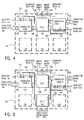
- FIG. 4 illustrates an unpopulated board with one electronic component card and a plurality of connector cards for testing and diagnostics purposes.
- FIG. 5 illustrates an unpopulated board comprising more than one unit-under-test attached to a plurality of connector cards in the process of being diagnosed.
- FIGS. 6A and 6B show a flow chart which summarizes the various steps for diagnosing a populated board comprised of hybrid electrical components.
- the broad overall concept of the present invention applies to a pre-wired board 100 of the type illustrated in FIG. 1.
- This board has a plurality of electronic components mounted thereon including cards 101, modules or multi-chip modules, 102 and 103, dip packaged components 104, etc.
- These components are of a mixed nature, origin and technology, both, at the chip and at the module level.
- these modules may follow a strict set of design for testability rules, or may incorporate characteristics that apply to a structured design.
- Others may be vendor components with a unique function whereby economic considerations may preclude a designer from incorporating extra circuitry that potentially could increase cost. All these components are then mounted on the board 100 and arranged in a manner so as to increase its performance and operation.
- Each board 100 has at least one I/O socket 105 which has a plurality of input/output pins which are wired to various points on the board 100 and provides the mechanism for connecting signals to and from the board and the external system elements.
- a plurality of such boards may eventually end up populating one or several frames that form a complex system. The efficiency of the overall package helps to determine the performance of the system. Too often, though, little thought and consideration is given to the testability at the various packaging levels, and even less perhaps, to the ease of diagnosing a failing component.
- each pin on each component mounted on the board 100 be connectable during testing thereof either to a shift-register latch (SRL), or to a board input/output pin.
- the SRL can be located either on the multi-chip module such as 102, 103 and cards 101, or on a connector card that is inserted in an empty socket (not shown) made vacant by removal of a component on the board 100 during test or any combination thereof.
- all the SRLs are wired together in series so that data can be scanned in or out of the SRLs through one board I/O pin.
- Clocking is also required so a total of four board level I/O pins must be dedicated to the testing/diagnosing functions described herein when an SRL is involved.
- the remaining board I/O pins can be coupled by a connector card to I/O pins of the component under test.
- a connector card 110 as illustrated in Fig. 2 is utilized to provide the mechanism for testing the components on the board 100.
- Each empty socket (not shown) produced by removal of one or more components from the board 100 has a plurality of I/O pins which are used to connect the board 100 I/O pins to I/O pins of the component under test.
- Each empty socket also has a plurality of pins which are each coupled to I/O pins of components remaining on the board 100 which are to be tested.
- the I/O pins of the component under test are coupled directly to the board I/O pins rendering the input pins of the component under test controllable from the board input pins and the output pins of the component under test observable from the board output pins.
- a socket (not shown) can be provided by design to aid in testing the circuit board.
- This socket will have a plurality of pins thereof coupled to a plurality of I/O pins of a component to be tested.
- the socket will also have a plurality of pins coupled to the board I/O pins.
- the component under test is not coupled to the board I/O pins.
- the I/O pins of the component under test are coupled to the board I/O pins rendering the input pins of the component under test controllable from the board I/O pins and the output pins of the component under test observable from the board I/O pins.
- a connector card 110 may have several types of circuits and electrical wiring thereon. The circuits and the wiring provide the electrical network to couple the board I/O pins to the I/O pins of the components on the board 100.
- a typical connector card 110 (FIG. 2) may have a number of direct connection wires 113 which function to couple the component input pins 116 to the board input pins 121, and component output pins 122 to the board output pins 117.
- the direct connection wires 113 can be used to test components having fewer or as many I/O pins as there are in the board connector 105 of Fig. 1.
- shift register latches (SRL) 111 to couple to the component inputs and shift register latches 111′ to couple to the component outputs.
- SRL shift register latches
- the output pins of the component under test are coupled to the output SRLs 111′ which latches the response of the component under test. That data is subsequently scanned out of the output SRLs 111′ via the board pins.
- Each SRL latch 111 on the upper edge of the card 110 in FIG.2 is connected to form a shift register chain called ISR (Input-Shift-Register) with the ISR Scan-in pin 119 feeding the first SRL of the chain, and the last SRL feeding the ISR scan-out pin 115.
- the ISR provides boundary-scan capabilities to the components on the board 100.
- the shifting operation is accomplished by a plurality of shift clock pulses on clock line 120.
- the clocking transfers data from one SRL to the next SRL serially. Data is inputted to each SRL 111 via connector card input pin 112, which are then attached via the socket on the board 100 to the component inputs that require boundary-scan latches.
- SRL's 111′ A similar arrangement of SRL's 111′ to the one previously described is used to form the Output-Shift-Register (OSR) chain shown on the bottom of FIG. 2.
- the OSR scanin line 123 feeds the first SRL 111′ in the OSR chain.
- the last SRL 111′ of the OSR chain feeds the OSR scan-out line 118.
- Shift clocks 120 are used to shift the data contained in the OSR chain.
- Data is inputted to each SRL 111′ of the OSR chain via the connector card input pin 114 which are connected via the socket on the board 100 to the component outputs that require boundary-scan latches.
- the SRL blocks 111, 111′ of FIG.2 can be either a simple master-slave shift register latch L1/L2, 130/131 (FIG. 3) or a doubled buffer arrangement L1/L2/L3, 133/134/135, called SSRL (Stable Shift Register Latch) 132.
- the SSRL's 132 are used to interface with sequential circuits within the logic, in the event of a non-structured design that ordinarily lacks the SRL arrangements previously described, whereas the simpler SRL latches 111, 111′ are used to interface with combinatorial elements within the logic.
- latches L1/L2 133/134 are used to shift in the desired test pattern, with clock C3 136 off to ensure that the shift sequences do not disturb the test patterns stored in latch L3 135.
- the outputs from the buffer latch L3 135 feeding the sequential logic hold the values of test pattern n while test pattern n+1 is shifted in from ISR Scan-in line 119 of FIG. 2.
- clock C3, 136 is enabled, test pattern n+1 is applied to the sequential logic. This arrangement ensures race-free testing of the modules/cards containing sequential logic circuitry. All other lines inputting to the L1 latches 130 are well known to the state of the art and will not be further discussed. Additional information on the aforementioned lines and operation of the latches coupled thereto are fully described in U.S.-A 3.806.891, 3.761.695, 3.783.254, and 3.784.907.
- the present invention involves a new method of testing components in situ.
- the first aspect of the invention involves isolating a component mounted on the circuit board from other components on the board. This is done by removing components from the board which couple to the input/output pins of the component suspected of failing.
- one or more connector cards are mounted on the board by plugging them into the socket(s) vacated by removed components.
- the connector cards provide either direct connection or shift register latch coupling between the I/O's of the component suspected of failing and the board I/O's.
- test stimuli are applied to the suspected component via the board input pins and responses are recorded via the board output pin(s).
- the responses can thereafter be analyzed to determine if the suspected component is, in fact, a failing component.
- the present embodiment can be further expanded by including a self test mechanism on the connector card.
- the aforementioned ISR and OSR chains in FIG.2 can be configured as a LFSR (Linear Feedback Shift Register) and/or MISR (Multiple Input Shift Register) which are respectively used to generate a set of pseudo-random test patterns, and accumulating responses through signature compression and analysis, thus providing self-test capabilities to one or several groups of components on the board 100.
- An LFSR is illustrated in U.S. Patents 4,687,988 and 4,745,355. No further description of the self-test mechanism is required, since this is well known in the state of art, and fully described in U.S.-A 4.513.418 and 4.519.078 and the references cited therein which are all herein incorporated by reference.
- the presence of the aforementioned self-test circuitry on the connector cards allows for real-time in-situ diagnostics of the unit under test which may comprise a single or a plurality of components.
- the board 100 of Fig. 1 is initially tested unpopulated. Each component, prior to its mounting on the board is also individually tested. Once fully populated, the board is tested by applying a stream of test instructions to the populated board 100 through the board I/O's until a failure is recorded. This is a functional test. Once a failure is detected the objective becomes to recreate the failing conditions by reapplying a subset of the original test instructions. If the subset fails to recreate this failing condition, it is augmented by an additional subset of n immediately preceding test instructions from the original test set. This process is repeated until the failed condition is replicated. The set of test instructions thus obtained is then used by a logic simulator to extract test patterns (and expected responses) at the board component boundaries for each of the m components on the board 100.
- the extracted test patterns Ti are applied to each of the m board components via the combination of: 1. direct board inputs which are connected to the unit under test (UUT) 141 via lines 148, 2. connector board input pins 158 are coupled to the connector card 140 via cable 146, which, in turn, are attached to the UUT 141 via cable 156 through the connector card 140, and 3. boundary scan-in line 147 through the ISR chain 143 whose outputs feed the UUT 141 via cable 155.
- the output responses are observed via the combination of: 1. direct board outputs which are connected to the UUT 141 via lines 149, 2. connector board output pins are coupled to the connector card 142 via cable 145, which, in turn, are attached to the UUT 141 via cable 150 through connector card 142, and 3. boundary scan-out line 152 through the OSR chain 153 whose inputs are fed from the UUT 141 via the cable 150.
- the UUT 141 can be tested unit-in-place using the embedded wires on the circuit board 100 provided that all other modules on the board communicating with UUT 141 are replaced with appropriate connector cards.
- a defective board component is thus isolated and identified when the applied test Ti fails.
- the same test pattern set can be used to further diagnose the identified failed board component(s) down to failing chip(s) or failing circuit contained therein. Oftentimes, additional test patterns may be required particularly when diagnosis down to a failing circuit within a chip is desired.
- the unit-in-place diagnostics methodology of the present invention employs the following steps: (1) Removing at least one component from the circuit board. (2) Installing in the socket(s) vacated by the removed component(s) a coupling means to couple I/O pins of a selected component remaining on the circuit board with board I/O pins. (3) Applying a plurality of test instructions to the selected component via the board input pins. (4) Storing the response signals received from the selected component at the circuit board output pins in response to the applied test instructions. (5) Comparing the stored response signals with expected response signals. (6) Indicating the selected component as failing when the expected response signals and stored response signals are not identical.
- the aforementioned unit-in-place diagnostics set-up and methodology can be extended to an expanded unit under test that is comprised of a selected group of interacting modules/cards on the board 100 as shown in FIG. 5.
- FIGs. 6A and 6B comprise a flow-chart which summarizes the board diagnostic method using the present invention.
- FIGs. 6A and 6B are comprised of the following six steps:
- some of the components mounted on the board 100 of Fig. 1 may be mounted in a socket on the board. If such component has at least three or four input/output pins which are connected to the board input/output pins, the component can be removed from the socket and a connector card placed therein.
- the connector card may include jumper wires between selected board I/O pins coupled to the socket and I/O pins from components not removed from the board.
- the connector card may also have a plurality of shift register latches thereon. These latches are coupled to the board I/O pins and to the input/output pins of components not removed from the board.
- the function of the connector card in this alternative is the same as described earlier. The principal difference in this configuration is that jumper wires are used in lieu of board interconnections to test the UUT.
- Another alternative configuration occurs when at least one of the components mounted on the board 100 are designed with LSSD or boundary scan design rules.
- the component has a shift register latch for assisting in testing the component.
- a connector card is provided with a shift register latch thereon. When the card is mounted on the board, the card carried shift register latches become series-coupled with the component shift register latch(es). This provides the necessary means to use a combination of component internal SRL's on the connector card to perform diagnostics testing. In this fashion, test data can be scanned into numerous components on the board thereby permitting testing of more than one component during any given test.
Landscapes
- Engineering & Computer Science (AREA)
- General Engineering & Computer Science (AREA)
- Physics & Mathematics (AREA)
- General Physics & Mathematics (AREA)
- Theoretical Computer Science (AREA)
- Computer Hardware Design (AREA)
- Quality & Reliability (AREA)
- Tests Of Electronic Circuits (AREA)
- Test And Diagnosis Of Digital Computers (AREA)
Claims (11)
- System, um an Ort und Stelle fehlerhafte oder defekte Bauelemente zu isolieren und zu diagnostizieren, die auf einer Leiterplatte montiert sind, die eine Vielzahl von darauf montierten und miteinander verbundenen Bauelementen hat, wobei jedes Bauelement eine Vielzahl von Eingangs- und Ausgangsanschlüssen hat und die Leiterplatte eine Vielzahl von Leiterplatteneingangs- und -ausgangsanschlüssen hat, und das System dadurch gekennzeichnet ist, daß es folgendes umfaßt:- eine auf der Leiterplatte in einem Sockel montierbare Anschlußkarte, von der mindestens ein Bauelement, das normalerweise darauf montiert ist, entfernt worden ist, um ein ausgewähltes, auf der Leiterplatte verbleibendes Bauelement zu isolieren und prüfbar zu machen, indem man die Eingangsanschlüsse des ausgewählten Bauelements von den Eingangsanschlüssen der Leiterplatte steuerbar und die Ausgangsanschlüsse des ausgewählten Bauelements von den Ausgangsanschlüssen der Leiterplatte überwachbar macht, und die Karte folgendes umfaßt:- einen Stecker, um in den durch das entfernte Bauelement frei gewordenen Sockel den Sockel einzustecken, der eine Vielzahl von Anschlußstiften hat, wobei zumindest einige der Anschlußstifte mit den Eingangsund Ausgangsanschlüssen der Leiterplatte verbunden sind und zumindest einige der restlichen Anschlußstifte mit den Eingangs- und Ausgangsanschlüssen des ausgewählten Bauelements verbunden sind, und wobei sich auf der Karte, an welcher der Stecker angebracht ist, eine Vielzahl von Leitungen befindet, von denen jede dazu dient, einen der Anschlußstifte, der mit einem Eingangs- oder Ausgangsanschluß der Leiterplatte verbunden ist, mit einem Anschlußstift zu verbinden, der mit einem Eingangs- oder Ausgangsanschluß des ausgewählten Bauelements verbunden ist.
- System nach Anspruch 1, wobei die auf der Leiterplatte montierbare Karte ein Schieberegister mit einer Vielzahl von Stufen enthält, einen Taktschaltkreis, der mit allen Stufen verbunden ist, um Daten von einer Stufe zur nächsten zu leiten, einen Ausgang von jeder Stufe, der mit einem Eingangsanschluß des ausgewählten Bauelements verbunden ist, einen Schieberegister-Dateneingang, der mit einem Eingangsanschluß der Leiterplatte verbunden ist, und wobei der Taktschaltkreis mit einem Eingangsanschluß der Leiterplatte verbunden ist, wodurch es einer Vielzahl von Eingangsanschlüssen des ausgewählten Bauelements möglich wird, Daten von einem einzigen Leiterplatten-Eingangsanschluß zu empfangen.
- System nach Anspruch 1, wobei die auf der Leiterplatte montierbare Karte ein Schieberegister mit einer Vielzahl von Stufen enthält, einen Taktschaltkreis, der mit allen Stufen verbunden ist, um Daten von einer Stufe zur nächsten zu leiten, einen Eingang zu jeder Stufe, der mit einem Ausgangsanschluß des ausgewählten Bauelements verbunden ist, einen Schieberegister-Datenausgang, der mit einem Ausgangsanschluß der Leiterplatte verbunden ist, und wobei der Taktschaltkreis mit zumindest einem Eingangsanschluß der Leiterplatte verbunden ist, um von dort Taktimpulse zu empfangen, wodurch es möglich wird, eine Vielzahl von Ausgangsanschlüssen des ausgewählten Bauelements an einem einzigen Ausgangsanschluß der Leiterplatte zu überwachen.
- System nach Anspruch 2, wobei die auf der Leiterplatte montierbare Karte ein zweites Schieberegister mit einer Vielzahl von Stufen enthält, einen zweiten Taktschaltkreis, der mit allen Stufen des zweiten Schieberegisters verbunden ist, um Daten von einer Stufe zur nächsten zu leiten, einen Eingang zu jeder Stufe des zweiten Schieberegisters, der mit einem Eingangsanschluß des ausgewählten Bauelements verbunden ist, einen Schieberegisterausgang, der mit einem Ausgangsanschluß der Leiterplatte verbunden ist, und wobei der zweite Taktschaltkreis mit einem Eingangsanschluß der Leiterplatte verbunden ist, um dort Taktimpulse zu empfangen, wodurch es möglich wird, daß eine Vielzahl von Ausgangsanschlüssen des ausgewählten Bauelements an einem einzigen Ausgangsanschluß der Leiterplatte überwacht werden kann.
- System, um an Ort und Stelle ein Bauelement einer Vielzahl von Bauelementen mit jeweils einer Vielzahl von Eingangs-/Ausgangsanschlüssen zu testen, die auf einer Leiterplatte montiert sind, wobei mindestens ein Bauelement auf eine Art und Weise konzipiert ist, die weder niveauempfindlichen Abtastentwurfs-(LSSD-)Regeln noch Boundary-Scan-Entwurfsregeln entspricht, die Leiterplatte eine Vielzahl von Eingangs-/Ausgangsanschlüssen hat und das System dadurch gekennzeichnet ist, daß es folgendes umfaßt:
ein Verbindungsmittel zur Montage auf der Leiterplatte, wenn zumindest ein Bauelement von der Leiterplatte entfernt worden ist, wobei das entfernte Bauelement auf der Leiterplatte mit zumindest einem Eingangs-/Ausgangsanschluß eines ausgewählten, von der Leiterplatte nicht entfernten Bauelements über Leitungen verbunden war, das ausgewählte Bauelement weder LSSD- noch Boundary-Scan-Entwurfsregeln entspricht, das entfernte Bauelement auf der Leiterplatte mit zumindest einem Eingangs-/Ausgangsanschluß der Leiterplatte über Leitungen verbunden war, das Verbindungsmittel Mittel enthält, um zumindest einen Eingangs-/Ausgangsanschluß der Leiterplatte mit zumindest einem Eingangs-/Ausgangsanschluß des ausgewählten Bauelements zu verbinden, wodurch es möglich wird, daß zumindest einige der Eingangs-/Ausgangsanschlüsse des ausgewählten Bauelements direkt von den Eingangs-/Ausgangsanschlüssen der Leiterplatte getestet werden können;
und wobei das Verbindungsmittel eine mehrstufige Schieberegisterkippstufe enthält, die mit einem Eingangs-/Ausgangsanschluß der Leiterplatte und einer Vielzahl der Eingangs-/Ausgangsanschlüsse des ausgewählten Bauelements verbunden ist, wobei die Schieberegisterkippstufe eine Taktsteuerschaltung für den Empfang von Taktsignalen von mindestens einem Eingangs-/Ausgangsanschluß der Leiterplatte hat, um Signale von der einen Stufe zur nächsten Stufe durchzulassen. - System nach Anspruch 5, das eine zweite mehrstufige Schieberegisterkippstufe enthält, wobei jede Stufe der ersten Schieberegisterkippstufe mit einigen Eingangs-/Ausgangsanschlüssen des ausgewählten Bauelements verbunden ist und die Stufen des zweiten Schieberegisters mit anderen Eingangs-/Ausgangsanschlüssen des ausgewählten Bauelements verbunden sind und wobei die zweite Schieberegisterkippstufe eine Taktsteuerschaltung für den Empfang von Taktsignalen von mindestens einem Eingangs-/Ausgangsanschluß der Leiterplatte hat, um Signale von der einen Stufe der zweiten Schieberegisterkippstufe zur nächsten Stufe der zweiten Schieberegisterkippstufe durchzulassen.
- System nach Anspruch 1 oder 5, das des weiteren einen Pseudozufallstestmuster-Generator enthält, der auf der Karte angeordnet ist, die auf der Leiterplatte montiert werden kann, wobei der Testmustergenerator auf Signale an ausgewählten Eingangsanschlüssen der Leiterplatte anspricht, die mit ihm verbunden sind, um mindestens ein Testmuster für Eingangsanschlüsse des ausgewählten Bauelements zu erzeugen.
- System nach Anspruch 7, das ein Signaturregister enthält, das auf der Karte angeordnet ist, die auf der Leiterplatte montiert werden kann, wobei das Signaturregister in der Praxis angeschlossen ist, um Signale von Ausgangsanschlüssen des ausgewählten Bauelements zu empfangen und zu akkumulieren und das Signaturregister mit Ausgangsanschlüssen der Leiterplatte verbunden ist, wodurch der Inhalt des Signaturregisters von einem Ausgangsanschluß der Leiterplatte überwacht werden kann.
- Verfahren zur Isolierung und Diagnose von fehlerhaften oder defekten Bauelementen an Ort und Stelle, die auf einer Leiterplatte montiert sind, die eine Vielzahl von miteinander verbundenen, darauf montierten Bauelementen hat, wobei jedes Bauelement eine Vielzahl von Eingangs- und Ausgangsanschlüssen und die Leiterplatte eine Vielzahl von Leiterplatten-Eingangs-/Ausgangsanschlüssen hat ufd das Verfahren die folgenden Schritte umfaßt:- Entfernen von mindestens einem Bauelement von der Leiterplatte, wobei das zumindest eine entfernte Bauelement normalerweise in einem Sockel auf der Leiterplatte montiert ist;- Installieren einer Anschlußkarte gemäß dem Isolierungs- und Diagnosesystem nach jedwedem der Ansprüche 1 bis 4 und 7 bis 8 anstelle des zumindest einen entfernten Bauelements, wobei die Anschlußkarte Mittel bereitstellt, um mindestens einige der Eingangs-/Ausgangsanschlüsse eines ausgewählten Bauelements, das auf der Leiterplatte montiert ist, mit einigen der Eingangs-/Ausgangsanschlüsse der Leiterplatte zu verbinden;- Anlegen von Testmustern an zumindest einige der Eingangs-/Ausgangsanschlüsse der Leiterplatte, die mit dem ausgewählten Bauelement verbunden sind; und- Registrieren der Antwortsignale von dem ausgewählten Bauelement an zumindest einigen der Eingangs-/Ausgangsanschlüsse der Leiterplatte als Antwort auf die Testmuster.
- Verfahren zum Testen von Bauelementen einer Leiterplatte an Ort und Stelle, die eine Vielzahl von miteinander verbundenen, darauf montierten Bauelementen hat, wobei jedes Bauelement eine Vielzahl von Eingangs- und Ausgangsanschlüssen hat, und das Verfahren die folgenden Schritte umfaßt :- Entfernen von mindestens einem Bauelement von der Leiterplatte, wobei das zumindest eine entfernte Bauelement normalerweise in einem Sockel auf der Leiterplatte montiert ist;- Installieren einer Anschlußkarte gemäß dem Testsystem nach einem beliebigen der Ansprüche 5 bis 8, die auf der Leiterplatte in dem Sockel montiert werden kann, der durch das zumindest eine entfernte Bauelement frei geworden ist, um Signale von Eingangsanschlüssen der Leiterplatte mit den Eingangsanschlüssen eines ausgewählten, auf der Leiterplatte verbleibenden Bauelements zu verbinden und um Signale von Ausgangsanschlüssen des ausgewählten Bauelements mit Ausgangsanschlüssen der Leiterplatte zu verbinden;- Anlegen einer Reihe von Prüfbefehlen an Ort und Stelle, um ein ausgewähltes Leiterplatten-Bauelement über die Eingangsanschlüsse der Leiterplatte zu testen;- Speichern der Antwortsignale an den Ausgangsanschlüssen der Leiterplatte, die von den Ausgangsanschlüssen des ausgewählten Bauelements empfangen werden, wobei die Antwortsignale als Antwort auf die Reihe von Prüfbefehlen erzeugt werden;- Vergleichen der gespeicherten Antwortsignale mit erwarteten Antwortsignalen; und- Angeben des ausgewählten Bauelements als defekt, wenn die Antwortsignale nicht mit den erwarteten übereinstimmen.
- Verfahren zum Testen einer Leiterplatte mit einer Vielzahl von miteinander verbundenen, darauf montierten Bauelementen, wobei jedes Bauelement eine Vielzahl von Eingangs- und Ausgangsanschlüssen hat und das Verfahren die folgenden Schritte umfaßt:a) Testen einer vollbestückten Leiterplatte mit einer kompletten Reihe von Prüfbefehlen T, wobei die komplette Reihe von Prüfbefehlen in Untergruppen variabler Länge unterteilt wird, bis ein Fehler während der Ausführung der Testuntergruppe TF festgestellt wird;b) Erneutes Testen der vollbestückten Leiterplatte mit der Testuntergruppe TF, die um zunehmend frühere Testuntergruppen erhöht wird, bis der Fehler wieder festgestellt wird;c) Simulieren der Logik der vollbestückten Leiterplatte mit allen Testuntergruppen, die zur Wiedergabe des festgestellten Fehlers gefunden werden, und Entnehmen der simulierten Signalwerte an jedem der Eingangs-/Ausgangsanschlüsse des Leiterplatten-Bauelements, um eine Reihe von Prüfbefehlen für jedes Bauelement auf der Leiterplatte zu bilden; undd) Diagnostizieren der defekten Leiterplatte, indem das Prüfverfahren nach Anspruch 10, bei dem die Packung an Ort und Stelle über die Anschlußstifte getestet wird, auf jedes Bauelement auf der Leiterplatte angewendet wird, wobei die im Schritt c) festgelegten Prüfbefehle für jedes der Bauelemente auf der Leiterplatte verwendet werden.
Applications Claiming Priority (2)
| Application Number | Priority Date | Filing Date | Title |
|---|---|---|---|
| US07/267,409 US4963824A (en) | 1988-11-04 | 1988-11-04 | Diagnostics of a board containing a plurality of hybrid electronic components |
| US267409 | 1988-11-04 |
Publications (3)
| Publication Number | Publication Date |
|---|---|
| EP0367710A2 EP0367710A2 (de) | 1990-05-09 |
| EP0367710A3 EP0367710A3 (de) | 1991-09-04 |
| EP0367710B1 true EP0367710B1 (de) | 1995-05-17 |
Family
ID=23018645
Family Applications (1)
| Application Number | Title | Priority Date | Filing Date |
|---|---|---|---|
| EP89480167A Expired - Lifetime EP0367710B1 (de) | 1988-11-04 | 1989-10-24 | Diagnostika einer Leiterplatte mit einer Mehrzahl elektronischer Hybridbauelemente |
Country Status (4)
| Country | Link |
|---|---|
| US (1) | US4963824A (de) |
| EP (1) | EP0367710B1 (de) |
| JP (1) | JP2505049B2 (de) |
| DE (1) | DE68922695T2 (de) |
Families Citing this family (27)
| Publication number | Priority date | Publication date | Assignee | Title |
|---|---|---|---|---|
| US5068603A (en) * | 1987-10-07 | 1991-11-26 | Xilinx, Inc. | Structure and method for producing mask-programmed integrated circuits which are pin compatible substitutes for memory-configured logic arrays |
| JP2561164B2 (ja) * | 1990-02-26 | 1996-12-04 | 三菱電機株式会社 | 半導体集積回路 |
| JPH0454607A (ja) * | 1990-06-22 | 1992-02-21 | Fanuc Ltd | 数値制御装置の分線プリント板 |
| US5498972A (en) * | 1990-08-15 | 1996-03-12 | Telefonaktiebolaget Lm Ericsson | Device for monitoring the supply voltage on integrated circuits |
| US5198759A (en) * | 1990-11-27 | 1993-03-30 | Alcatel N.V. | Test apparatus and method for testing digital system |
| US5321277A (en) * | 1990-12-31 | 1994-06-14 | Texas Instruments Incorporated | Multi-chip module testing |
| US5132635A (en) * | 1991-03-05 | 1992-07-21 | Ast Research, Inc. | Serial testing of removable circuit boards on a backplane bus |
| DE4110551C1 (de) * | 1991-03-30 | 1992-07-23 | Ita Ingenieurbuero Fuer Testaufgaben Gmbh, 2000 Hamburg, De | |
| US5323107A (en) * | 1991-04-15 | 1994-06-21 | Hitachi America, Ltd. | Active probe card |
| FI89223C (fi) * | 1991-10-03 | 1993-08-25 | Nokia Mobile Phones Ltd | Digitalt audiointerface i gsm-anordning |
| US5410551A (en) * | 1992-01-02 | 1995-04-25 | Andahl Corporation | Net verification method and apparatus |
| US5448166A (en) * | 1992-01-03 | 1995-09-05 | Hewlett-Packard Company | Powered testing of mixed conventional/boundary-scan logic |
| US5260649A (en) * | 1992-01-03 | 1993-11-09 | Hewlett-Packard Company | Powered testing of mixed conventional/boundary-scan logic |
| TW253097B (de) * | 1992-03-02 | 1995-08-01 | At & T Corp | |
| GB9212646D0 (en) * | 1992-06-15 | 1992-07-29 | Marconi Instruments Ltd | A method of and equipment for testing the electrical conductivity of a connection |
| GB9217728D0 (en) * | 1992-08-20 | 1992-09-30 | Texas Instruments Ltd | Method of testing interconnections between integrated circuits in a circuit |
| US5390194A (en) * | 1993-11-17 | 1995-02-14 | Grumman Aerospace Corporation | ATG test station |
| EP0733910B1 (de) * | 1995-03-16 | 1996-12-11 | Siemens Aktiengesellschaft | Platine mit eingebauter Kontaktfühlerprüfung für integrierte Schaltungen |
| US5818251A (en) * | 1996-06-11 | 1998-10-06 | National Semiconductor Corporation | Apparatus and method for testing the connections between an integrated circuit and a printed circuit board |
| US5841788A (en) * | 1996-10-18 | 1998-11-24 | Lucent Technologies Inc. | Methods for backplane interconnect testing |
| JPH10150514A (ja) * | 1996-11-18 | 1998-06-02 | Brother Ind Ltd | 画像読取装置、およびこの画像読取装置が備える光電変換部の調整装置 |
| US20030115502A1 (en) * | 2001-12-14 | 2003-06-19 | Smiths Industries Aerospace & Defense Systems, Inc. | Method of restoring encapsulated integrated circuit devices |
| JP2004108872A (ja) * | 2002-09-17 | 2004-04-08 | Sanyo Electric Co Ltd | 半導体パッケージ内部の結線テスト方法 |
| US7265534B2 (en) * | 2004-10-20 | 2007-09-04 | Freescale Semiconductor, Inc. | Test system for device characterization |
| US7350124B2 (en) * | 2005-10-18 | 2008-03-25 | International Business Machines Corporation | Method and apparatus for accelerating through-the pins LBIST simulation |
| US9400311B1 (en) * | 2015-03-31 | 2016-07-26 | Cadence Design Systems, Inc. | Method and system of collective failure diagnosis for multiple electronic circuits |
| KR102471771B1 (ko) * | 2020-11-20 | 2022-11-29 | 주식회사 에스디에이 | 고속 신호 특성 검증을 위한 지능형 프로브 카드 |
Family Cites Families (13)
| Publication number | Priority date | Publication date | Assignee | Title |
|---|---|---|---|---|
| US3924181A (en) * | 1973-10-16 | 1975-12-02 | Hughes Aircraft Co | Test circuitry employing a cyclic code generator |
| US4055806A (en) * | 1976-01-23 | 1977-10-25 | Patel Harshad M | Integrated circuit substitution device |
| US4475169A (en) * | 1982-02-01 | 1984-10-02 | Analog Devices, Incorporated | High-accuracy sine-function generator |
| US4465972A (en) * | 1982-04-05 | 1984-08-14 | Allied Corporation | Connection arrangement for printed circuit board testing apparatus |
| FR2531230A1 (fr) * | 1982-07-27 | 1984-02-03 | Rank Xerox Sa | Ensemble destine au test automatique centralise de circuits imprimes et procede de test de circuits a microprocesseur faisant application de cet ensemble |
| US4519078A (en) * | 1982-09-29 | 1985-05-21 | Storage Technology Corporation | LSI self-test method |
| US4513418A (en) * | 1982-11-08 | 1985-04-23 | International Business Machines Corporation | Simultaneous self-testing system |
| EP0196171B1 (de) * | 1985-03-23 | 1991-11-06 | International Computers Limited | Integrierte digitale Schaltungen |
| US4687988A (en) * | 1985-06-24 | 1987-08-18 | International Business Machines Corporation | Weighted random pattern testing apparatus and method |
| US4745355A (en) * | 1985-06-24 | 1988-05-17 | International Business Machines Corporation | Weighted random pattern testing apparatus and method |
| US4709366A (en) * | 1985-07-29 | 1987-11-24 | John Fluke Mfg. Co., Inc. | Computer assisted fault isolation in circuit board testing |
| US4701696A (en) * | 1985-11-25 | 1987-10-20 | Tektronix, Inc. | Retargetable buffer probe |
| FR2622711A1 (fr) * | 1987-11-04 | 1989-05-05 | Trt Telecom Radio Electr | Dispositif destine a remplacer un circuit integre comportant sur la meme puce un processeur de signal et un ensemble de memoire contenant des informations figees |
-
1988
- 1988-11-04 US US07/267,409 patent/US4963824A/en not_active Expired - Fee Related
-
1989
- 1989-10-20 JP JP1271888A patent/JP2505049B2/ja not_active Expired - Lifetime
- 1989-10-24 DE DE68922695T patent/DE68922695T2/de not_active Expired - Fee Related
- 1989-10-24 EP EP89480167A patent/EP0367710B1/de not_active Expired - Lifetime
Also Published As
| Publication number | Publication date |
|---|---|
| US4963824A (en) | 1990-10-16 |
| DE68922695T2 (de) | 1996-01-25 |
| EP0367710A3 (de) | 1991-09-04 |
| JPH02171668A (ja) | 1990-07-03 |
| EP0367710A2 (de) | 1990-05-09 |
| DE68922695D1 (de) | 1995-06-22 |
| JP2505049B2 (ja) | 1996-06-05 |
Similar Documents
| Publication | Publication Date | Title |
|---|---|---|
| US4963824A (en) | Diagnostics of a board containing a plurality of hybrid electronic components | |
| US4817093A (en) | Method of partitioning, testing and diagnosing a VLSI multichip package and associated structure | |
| US5852617A (en) | Jtag testing of buses using plug-in cards with Jtag logic mounted thereon | |
| US4503537A (en) | Parallel path self-testing system | |
| US5428624A (en) | Fault injection using boundary scan | |
| US6983441B2 (en) | Embedding a JTAG host controller into an FPGA design | |
| US6256760B1 (en) | Automatic test equipment scan test enhancement | |
| EP0930570B1 (de) | Verbindungsprüfung unter Verwendung von Leiterplatten-Topologiedaten | |
| EP0560500B1 (de) | Verfahren und Gerät zum Prüfen von Ein-/Ausgabeverbindungen des Randsteckverbinders einer Schaltkreiskarte mit Boundary Scan | |
| JPS6256528B2 (de) | ||
| US5487074A (en) | Boundary scan testing using clocked signal | |
| GB2186094A (en) | Self diagnostic cyclic analysis testing for lsi/vlsi | |
| Lubaszewski et al. | A pragmatic test and diagnosis methodology for partially testable MCMs | |
| GB2405945A (en) | Printed circuit board test apparatus | |
| De Jong et al. | Boundary scan test, test methodology, and fault modeling | |
| US20030149913A1 (en) | Method and apparatus for efficient burn-in of electronic circuits | |
| Hsu et al. | Selective controllability: A proposal for testing and diagnosis | |
| Fasang | Boundary scan and its application to analog-digital ASIC testing in a board/system environment | |
| O’GRADY et al. | Issues in the testability of printed wiring boards | |
| Hughes et al. | Effects of packaging and interconnect technology on testability of printed wiring boards | |
| Zorian | Fundamentals of MCM testing and design-for-testability | |
| Zorian | Multi-chip module technology | |
| Bennetts | IEEE 1149.1 JTAG and Boundary-Scan Tutorial | |
| Ziaja | Using LSSD to test modules at the board level | |
| TW202524495A (zh) | Jtag標準接腳測試系統 |
Legal Events
| Date | Code | Title | Description |
|---|---|---|---|
| PUAI | Public reference made under article 153(3) epc to a published international application that has entered the european phase |
Free format text: ORIGINAL CODE: 0009012 |
|
| AK | Designated contracting states |
Kind code of ref document: A2 Designated state(s): DE FR GB |
|
| 17P | Request for examination filed |
Effective date: 19900926 |
|
| PUAL | Search report despatched |
Free format text: ORIGINAL CODE: 0009013 |
|
| AK | Designated contracting states |
Kind code of ref document: A3 Designated state(s): DE FR GB |
|
| 17Q | First examination report despatched |
Effective date: 19921230 |
|
| GRAA | (expected) grant |
Free format text: ORIGINAL CODE: 0009210 |
|
| AK | Designated contracting states |
Kind code of ref document: B1 Designated state(s): DE FR GB |
|
| REF | Corresponds to: |
Ref document number: 68922695 Country of ref document: DE Date of ref document: 19950622 |
|
| ET | Fr: translation filed | ||
| PGFP | Annual fee paid to national office [announced via postgrant information from national office to epo] |
Ref country code: FR Payment date: 19951009 Year of fee payment: 7 |
|
| PGFP | Annual fee paid to national office [announced via postgrant information from national office to epo] |
Ref country code: DE Payment date: 19951030 Year of fee payment: 7 |
|
| PLBE | No opposition filed within time limit |
Free format text: ORIGINAL CODE: 0009261 |
|
| STAA | Information on the status of an ep patent application or granted ep patent |
Free format text: STATUS: NO OPPOSITION FILED WITHIN TIME LIMIT |
|
| 26N | No opposition filed | ||
| PGFP | Annual fee paid to national office [announced via postgrant information from national office to epo] |
Ref country code: GB Payment date: 19960925 Year of fee payment: 8 |
|
| PG25 | Lapsed in a contracting state [announced via postgrant information from national office to epo] |
Ref country code: FR Effective date: 19970630 |
|
| PG25 | Lapsed in a contracting state [announced via postgrant information from national office to epo] |
Ref country code: DE Effective date: 19970701 |
|
| REG | Reference to a national code |
Ref country code: FR Ref legal event code: ST |
|
| PG25 | Lapsed in a contracting state [announced via postgrant information from national office to epo] |
Ref country code: GB Free format text: LAPSE BECAUSE OF NON-PAYMENT OF DUE FEES Effective date: 19971024 |
|
| GBPC | Gb: european patent ceased through non-payment of renewal fee |
Effective date: 19971024 |