EP0367952A2 - Système pour détecter et analyser des objets arrondis - Google Patents
Système pour détecter et analyser des objets arrondis Download PDFInfo
- Publication number
- EP0367952A2 EP0367952A2 EP89117215A EP89117215A EP0367952A2 EP 0367952 A2 EP0367952 A2 EP 0367952A2 EP 89117215 A EP89117215 A EP 89117215A EP 89117215 A EP89117215 A EP 89117215A EP 0367952 A2 EP0367952 A2 EP 0367952A2
- Authority
- EP
- European Patent Office
- Prior art keywords
- pixels
- tangent
- pixel
- group
- trimming
- Prior art date
- Legal status (The legal status is an assumption and is not a legal conclusion. Google has not performed a legal analysis and makes no representation as to the accuracy of the status listed.)
- Granted
Links
Images


Classifications
-
- G—PHYSICS
- G06—COMPUTING OR CALCULATING; COUNTING
- G06T—IMAGE DATA PROCESSING OR GENERATION, IN GENERAL
- G06T7/00—Image analysis
- G06T7/0002—Inspection of images, e.g. flaw detection
- G06T7/0004—Industrial image inspection
-
- G—PHYSICS
- G06—COMPUTING OR CALCULATING; COUNTING
- G06T—IMAGE DATA PROCESSING OR GENERATION, IN GENERAL
- G06T7/00—Image analysis
- G06T7/60—Analysis of geometric attributes
- G06T7/62—Analysis of geometric attributes of area, perimeter, diameter or volume
-
- G—PHYSICS
- G06—COMPUTING OR CALCULATING; COUNTING
- G06V—IMAGE OR VIDEO RECOGNITION OR UNDERSTANDING
- G06V10/00—Arrangements for image or video recognition or understanding
- G06V10/40—Extraction of image or video features
- G06V10/44—Local feature extraction by analysis of parts of the pattern, e.g. by detecting edges, contours, loops, corners, strokes or intersections; Connectivity analysis, e.g. of connected components
- G06V10/443—Local feature extraction by analysis of parts of the pattern, e.g. by detecting edges, contours, loops, corners, strokes or intersections; Connectivity analysis, e.g. of connected components by matching or filtering
-
- G—PHYSICS
- G06—COMPUTING OR CALCULATING; COUNTING
- G06T—IMAGE DATA PROCESSING OR GENERATION, IN GENERAL
- G06T2207/00—Indexing scheme for image analysis or image enhancement
- G06T2207/30—Subject of image; Context of image processing
- G06T2207/30108—Industrial image inspection
- G06T2207/30141—Printed circuit board [PCB]
Definitions
- This invention relates to automatic image processing and more particularly, to a system for automatic image processing which enables features of rounded objects to be analyzed and characterized.
- the generic-property approach also takes two forms. One is based on the notion that idealized circuit features are simple, regular geometric shapes whereas defects typically are not. With this approach the system looks for unexpected irregular features.
- the second form is based on directly verifying design rules, e.g., trace width, feature spacing, pad locations and size, etc. In both forms, defects are usually detected by using strictly local neighborhood processing throughout the test image.
- the Broadbent, Jr. et al system is effective and provides the desired level of inspection capability. However, if substantial throughputs are required of reasonably complex items to be inspected, the performance capability of the Broadbent, Jr. et al. type system is rapidly out-distanced by the product flow.
- MITE Machine Image Transform Engine
- a system determines the characteristics of a substantially rounded feature, such as a via-hole in a printed circuit board.
- the system includes means for providing a serial flow of a raster scan image of pixels which represents the rounded feature.
- Means are further provided which select groups (i.e., neighborhoods) of pixels from the scan image, each group including pixels clustered about a plurality of chosen azimuths and lying about a line which is substantially tangent to a boundary of the rounded feature.
- Means are further provided to trim each selected group of pixels to eliminate pixels not lying on the tangent line.
- the pixels which remain after the trim operation are representative of the limits (e.g., diameter, radius, etc.) of the rounded feature and enable analyzing means to determine the characteristics of the rounded feature by examining the relationships between the tangent line pixels.
- a somewhat more sophisticated system is described which reduces the apparatus required for trimming the selected pixel groups.
- a tangent segment is fed into a plurality of parallel networks which initially identify right and left shoulders of the tangent segment. The identified ends are expanded and used as a mask to disconnect the central plateau of the original tangent segment from its next lower and non-central plateaus. Subsequent trimming enables the central plateau to be identified.
- each line of the scan is comprised of 10 pixel positions, with each succeeding scan line numbered sequentially.
- the pixel positions are numbered sequentially starting at the upper left and ending at the lower right. While there is shown only 10 horizontal scan pixel positions, it is common to have from 256 to 640 individual pixel positions per scan line and up to 512 scan lines. Of course, there are higher definition systems wherein both the number of pixels per scan line and the number of scan lines are greatly increased.
- pixels contained within the raster scan image are serially streamed through the various stages of the system and, at each stage, a "neighborhood" of pixels is operated upon by comparing it to a template or group of templates which define the logic function to be carried out.
- a "neighborhood" 50 of pixels clustered about center pixel 13 is shown and comprises pixels 2, 3, and 4 from scan line 0; pixels 12 and 14 from scan line 1, and pixels 22, 23 and 24 from scan line 2 (all shown in Fig. 1).
- each pixel is incremented by one position and an n+1 neighborhood 52 is created.
- each neighborhood pixel is as shown at 54 in Fig. 2 with each of the pixels (other than center pixel C) being denoted by the points of the compass.
- each pixel is represented by a logical 1 or 0 with a logical 1 indicating a dark area of the image and a logical 0 indicating a light area of the image.
- Image scanner 56 provides a pixel image of the device, circuit board or other feature being examined. If via-holes are being examined for their position and size, image scanner 56 will provide an image wherein the pixel points inside the via-hole have "1" indications and the surrounding areas have “0” indications. Essentially a "1" indication indicates the darker or inner areas of the via-hole and a "0" indicates a plane which is contiguous with the outside of the via-hole.
- image analyzer 58 which is comprised of a plurality of processing units, to be hereinafter described.
- Image analyzer 58 operates to isolate and reduce particular image features and provides a series of identified pixels on line 60 to controller 62. For instance, if image analyzer 58 is analyzing a via-hole configuration, it will, on line 60, provide a series of 4 or more pixels which identify the north, east, south and western tangents of the via-hole, with each pixel identified as to a specific address in the image scan.
- Controller 62 is then able, by using the addresses of the identified azimuthal pixels, to calculate the diameter of the via-hole, determine its placement in relation to other known features on the circuit board, and generally examine the contours of the hole, since it is now able to precisely identify the expected circumference of the hole and determine whether it varies from a predetermined defined shape.
- Controller 62 also controls the operation of image analyzer 58 via line 64. For instance, controller 62 provides clocking signals to image analyzer 58 which enables the serial pixel image to be synchronously clocked therethrough, so that each pixel 8-neighborhood is sequentially acted upon by the various serial processing units within image analyzer 58. Controller 62 is also employed, in the well known manner, to control the operation of image scanner 56 via line 66.
- FIG. 4 a block diagram of a processing element is illustrated and is the basic logical element utilized throughout image analyzer 58.
- the structure of the processing element shown in Fig. 4 is known in the prior art.
- a serial pixel image appears on input line 70 in the form of a serial stream of pixels arranged in increasing time order.
- the pixel stream passes through a series of three position, serial shift registers 72, 74 and 76.
- the output from serial shift register 72 is fed to the input of shift register 74 via a delay circuit 78.
- Delay circuit 78 may be a serial shift register having a number of pixel positions equal to the number of pixels in a raster scan line, less 3. (There are, of course, other ways of implementing delay circuit 78 which are well known to those skilled in the art).
- the output of serial shift register 74 is connected to the input of serial shift register 76 via delay circuit 80.
- the structure of delay circuit 80 is identical to that of delay circuit 78.
- Look up table 84 is essentially a random access memory which employs the bit indications on lines 82 as a nine bit address into its memory.
- the memory is configured to provide, for a particular 8-neighborhood input arrangement, an output bit consistent with a predetermined template.
- the template is pre-configured to provide a particular 8-neighborhood output in accordance with a desired function (e.g., "expansion”, “contraction”, “thinning”, etc.).
- a pixel bit (1 or 0) will be inserted into the first stage of serial shift register 72.
- a bit will be shifted out of the 3rd stage of serial shift register 72 and inserted into delay circuit 78.
- delay circuit 78 At the other end of delay circuit 78, a bit will emerge which will be inserted into the first stage of serial shift register 74 etc.
- the result of this action is that a new 8-neighborhood is created in shift registers 72, 74 and 76 each time a new pixel bit appears on input line 70.
- each 8-neighborhood being arranged as shown at 54 in Fig. 2, it is inverted and reversed by the circuit of Fig. 4 so that the northwestern bit of the neighborhood appears in the neighborhood's lower right corner with the southeastern bit appearing in the upper left hand corner.
- the western bit appears in the rightmost position of the neighborhood whereas the eastern bit appears in the leftmost position.
- templates which control the logical operation of each processing element. Each template is illustrated in accordance with the orientation of bits shown in Fig. 2 (and not Fig. 4).
- FIG. 5 there is shown a schematic of a via-hole 90 which has been greatly enlarged in size. Each of the small boxes shown in Fig. 5 is indicative of a pixel having a value equal to 1. It is to be noted that the via-hole encompasses 22 scan lines, each having a plurality of pixels which end at the circumference of the hole. For purposes of reference, the north, east, south and western azimuths of the via-hole are indicated in Fig. 5. The objective of the image analysis system is to determine the line of pixels which is tangent to one or more of the north, east, west or south extremities of the via-hole so that the hole's diameter and position can be accurately determined.
- FIG. 6 a block diagram of image analyzer 58 of Fig. 3 is shown.
- the two major portions of image analyzer 58 comprise the north, south, east and west tangent detector portion 60 and pixel identifier portion 62.
- Each of north, east, south and west tangent detectors 64, 66, 68 and 70 receives the input pixel stream.
- the outputs of the tangent detectors are provided in parallel to pixel position identification circuits 72, 74, 76 and 78 respectively.
- the output from each of the pixel position identification circuits is then fed to controller 62.
- FIG. 7 the north tangent detector 64 of Fig. 6 is shown in expanded detail. It should be understood that each of the tangent detectors is substantially identical except that each processing element's templates are modified in accordance with a particular azimuthal orientation.
- the north tangent detector identifies and works with pixels around an azimuth drawn through the north extremity of hole 90 (see Fig. 5); the east tangent detector operates upon and identifies pixels grouped around an azimuth drawn through the eastern most extremity of hole 90, etc.
- the operation of Fig. 7 will be described in conjunction with exemplary pixel images shown in Figs. 8a-8d and further, in conjunction with logic equations and templates illustrated in Figs. 13 et sequence.
- Each block shown in Fig. 7 represents a processing element which includes a template defined by the title within the block.
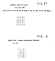
- Fig. 12 wherein is shown the definition of the symbols used with the logic equations and templates of Figs. 13-20. Bearing in mind those definitions, reference is also made to Figs. 13a-13d. Those Figs. illustrate the logic equations and templates which are used to identify and isolate the north, south, east and west pixels which lie on tangents to the circumference of a via-hole under examination.
- FIG. 8a An input pixel stream illustrating a via-hole is applied to input line 100 and "detect north tangent" processing element 102.
- a representation of the pixel scene, as it appears on line 100 is shown in Fig. 8a.
- each pixel square shown in Fig. 8a is represented by a 1 in the pixel stream, whereas the areas shown external to the hole are represented by 0's in the associated pixel positions.
- Ot CB and SWB and SB and SEB and (NOT(NEB or NB or NWB))
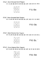
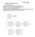
- pixel scene resulting from the operation of detect north tangent processing element 102 is shown in Fig. 8b and includes not only a series of 4 pixels 150 but several disconnected pixels 152 and 154.
- the next two stages of processing are employed to connect the disconnected pixels 152 and 154 to the plateau of pixels 150. This is accomplished by 8-expanding the pixel image shown in Fig. 8b to that shown in Fig. 8c so that the disjointed segments are merged. Then, the merged segments are thinned several times to achieve the single connected north tangent segment shown in Fig. 8d; and the merged segments are trimmed to result in a single north tangent segment which can then be identified as to its location (see Fig. 8e).
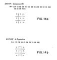
- the serial pixel output from processing element 102 is fed to 8-expansion processing element 104 where each pixel with a 1 bit has an 8-neighborhood constructed around it.
- the logic equation and template for the 8-expansion is shown in Fig. 14a.
- Fig. 14a As can be seen from an examination of Fig. 14a, if one input pixel of the 8-neighborhood is set to 1, then the output of 8-expansion processing element 104 is a 1 bit.
- Fig. 8c an 8 expansion creates a merging of the non-connected pixels shown in Fig. 8b and prepares the image for further processing.
- the expanded pixel scene is then applied to thinning processing elements 106, 108, 110 and 112 in sequence, with element 106 trimming top oriented pixels from the scene shown in Fig. 8c; element 108 trimming pixels on the right extremity of the scene shown in Fig. 8c; element 110 thinning pixels on the bottom of the scene shown in Fig. 8c and element 112 thinning pixels on the left of the image.
- the logic equations and templates for the thinning functions are found in Figs. 15a, 15b, 15c and 15d.
- the action of the respective thinning templates is to remove all but a sequence of connected 1 pixels from the image shown in Fig. 8c, with the result being the scene shown in Fig. 8d.
- processing element 106 provides a 1 output only when the conditions of the logic equation of Fig. 15a is satisfied.
- the AND NOT function shown there requires that the input 8-neighborhood center bit be set to 1 and that none of the five illustrated bit patterns be simultaneously present along with the 1 center pixel.
- processing element 106 provides a 0 output to the next thinning stage (thus "thinning" the image). In essence therefore, the scene is first thinned from the left, then from the bottom in processing element 108 where it is subjected to the templates shown in Fig.
- the thinned, serial image of pixels then passes to a multiplicity of trim stages 114 and 116 where the image in Fig. 8d is reduced to that in Fig. 8e.
- the equations and templates utilized by processing elements 114 and 116 for the trim functions are shown respectively in Fig. 16a and 16b.
- Trim processing elements appear in pairs and essentially nibble away pixels at either extremity of a run of pixels until there is just one left in the center.
- the number of trim processing elements required is dependent upon the estimated length of the sequence of thinned pixels and will vary in dependence upon the size of the image being examined.
- the trim function is arranged so as to not trim all pixels remaining in a scene. This is accomplished by the illustrated AND function.
- trim processing element 114 produces a 1 output. Otherwise, a 0 results. This prevents the situation from occurring where a single 1 pixel is found and trimmed.
- trim element 116 is not necessarily limited to 2, but rather is determined by the size of the hole, the expected run length of pixels resulting from the thinning effort, and the desired number of pixels remaining after trimming. Thus, for a hole of large diameter, a number of NNW trim stages would be interspersed with a number of SSE trim stages.
- Identification block 118 in Fig. 7 differs in structure from the aforementioned blocks. It identifies the position within the raster scan of the 1 or more pixels remaining after trimming. It includes a counter which commences a count at the moment of initiation of the raster scan and is reset at the termination of the raster scan. Thus, it is able to identify the position of an isolated 1-bit pixel by saving its count when the pixel appears. The saved count may then be converted to a Cartesian coordinate XY address through table look-up or another acceptable conversion process.
- the output from identification block 118 is fed to controller 62 for further processing.
- Each of the remaining tangent detectors (east, south and west) operate simultaneously, in parallel, with the north tangent detector and provide identified pixel outputs to controller 62.
- a modified tangent detector is shown which enables a reduction in the number of trim stages and thereby enables tangent identification to occur more rapidly.
- the initial processing portions of the system are not shown as they are identical to those shown in Fig. 7.
- the hole input pixel stream is fed through a series of blocks identical to blocks 102, 104, 106, 108, 110 and 112.
- the resulting thinned tangent segment pixel stream is then applied, via conductor 300 to three parallel networks. Those networks identify the right and left shoulders of the tangent plateau and, additionally, provide a delayed tangent segment for subsequent comparison and masking purposes.
- the operation of Fig. 9 will be described in conjunction with the pixel scenes shown in Figs.
- FIG. 9 illustrates the application of various logic stages to the thinned north tangent segment
- each of the other tangent segments (i.e., south, east and west) are processed in a substantially similar manner, using the templates and logic functions which apply thereto.
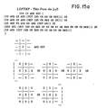
- a thinned north tangent segment (see Fig. 10a) is simultaneously applied to north left step processing element 302, north right step processing element 304 and two stage delay element 306. It is the function of north left step processing element 302 and north right step processing element 304 to identify and isolate in their pixel stream outputs, left and right shoulder portions 308 and 310 of the pixel scene of Fig. 10a.
- Right shoulder portion 310 is shown in Fig. 10b.
- Left shoulder portion 308 is isolated by processing element 302 and provides a similar left shoulder pixel stream (not illustrated).
- Dilation elements 312 and 314 dilate both the isolated right and left step pixel streams, to 2X2 pixel matrices to fill in some of the gaps therebetween. This is illustrated in Fig. 10c for the north right step.
- the outputs from dilation elements 312 and 314 are applied to a NOR circuit 316 and subsequently to AND circuit 318. They are also simultaneously applied to two additional dilation circuits 320 and 322.
- the output of NOR circuit 316 is the pixel stream shown in Fig. 10d wherein all pixel positions which were previously in the 1 state have been converted to 0 the state and vice versa.
- 2-stage delay 306 is a series of two processing elements which delay the thinned north tangent pixel stream an equivalent amount of time to that consumed by the operations of the north left step and north right step identification networks.
- pixels making up the thinned north tangent scene shown in Fig. 10a are applied to AND circuit 318 synchronously along with the pixel image emanating from NOR circuit 316. From an examination of Figs. 10a and 10d, it can be seen that the output of AND circuit 318 is as illustrated in Fig. 10e.
- the AND function is satisfied only for bits appearing in plateau 326 and for several isolated right and left step bits 328 and 330. While not shown in Fig. 10e, it is also possible that lower lying plateaus can occur as a result of the AND operation. Thus, further processing is required to assure that plateau 326 is properly isolated.
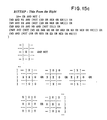
- pixel streams from southwest 2-dilate element 312 and southeast 2-dilate element 314 are applied to two additional dilation elements 320 and 322 respectively.
- the result is that the 2-dilations shown in Fig. 10c (and their mirror image, not shown) have additional dilation operations performed thereon resulting in the pixel scene shown in Fig. 10f (the left step dilation not being shown).
- the output from AND circuit 318 is applied through two trim processing elements 330 and 332 which act to remove the opposed end pixels from tangent pixel plateau 326 shown in Fig. 10e. Since pixels 328 and 330 stand alone, they are not removed, as trim elements 330 and 332 are restricted to removing pixels which are joined to another pixel.
- Delay elements 334 and 336 are inserted for the purpose of synchronizing the outputs from dilation elements 320 and 322 with trim element 332.
- the resulting outputs are applied to OR circuit 338 whose pixel stream output is the scene shown in Fig. 10g.
- left and right shoulders 342 and 346 are now completely connected and tangent plateau 348 is isolated therefrom.
- the output appearing on line 340 is applied to the circuit shown in Fig. 11, in parallel with outputs from the other three tangent detection circuits.
- Figs. 20a and 20b are shown in Figs. 20a and 20b respectively.
- the presence in an input neighborhood of center and north 1 bits and a 0 east bit; or center and northeast 1 bits and 0's in the north and east pixel positions give rise to a 1 output from the processing element.
- Such an output indicates the presence, in the input neighborhood, of a vertical step or step rising from the southwest to the northeast - thus indicating a "north left step". Any other bit pattern passing through north left step processing element 302 is eliminated.
- the north right step element 304 operates in a similar manner but in accordance with the equation and templates shown in Fig. 20b. Additionally, other, non-illustrated, south, west, and east step detection networks operate similarly, but in accordance with the equations and templates shown in Figs. 20c, 20d, 20e, 20f, 20g and 20h. It should be noted with respect to the west and east step processing elements, that the concept of left and right steps is eliminated and, due to the fact that the east and west tangent plateaus are vertically oriented, the steps on either side thereof become the top and bottom steps.
- Southwest 2-dilate processing element 312 and southeast 2-dilate processing element 314 employ the logic equations and templates shown in Figs. 19a and 19b respectively.
- southwest 2-dilate element 312 will provide a 1 output if its input neighborhood exhibits a 1 in one, or more of the center bit, east bit, northeast bit, or north bit. This results in an expansion of each 1 bit pixel to a neighborhood of 4 pixels, all of which are set to 1 and are oriented to the east, south and southeast direction from the original 1 bit pixel.
- the northwest 2-dilate and northeast 2-dilate logic equations and templates of Figs. 19 and 19d are employed in the operation of the south tangent segment detection circuit, whereas the east and west tangent detection circuits use combinations of the 2-dilate circuits, as appropriate.
- Each delay circuit e.g., 2-stage delay 306 and 1-stage delay 336) implements the center bit identity equation and template shown in Fig. 18.
- any such processing element repeats the incoming bit stream, delayed in time by the duration required for a processing element to operate on an input 8-neighborhood of pixels and is used for circuit synchronization.
- Trim 1-join processing elements 330 and 332 employ the equations and templates shown in Figs. 16a and 16b that have been previously described with respect to the operation of the circuit of Fig. 7 and will not be further considered here.
- the inputs on lines 340, 350, 360 and 370 take the form of a pixel scene such as shown in Fig. 10g.
- the scene for each of the east, south, and west tangents are identical to the north tangent scene in Fig. 10g but they are oriented appropriately around azimuth lines which pass through the east, south, and west points of the via-hole image.
- OR circuit 380 The output of OR circuit 380 is a pixel image which includes 4 plateaus of pixels (e.g., see plateau 348 in Fig. 10g) and clusters of shoulder pixels associated therewith, but separated therefrom. This pixel scene then passes through N stage trim processing element 382 where the end pixels appended to each plateau are successively trimmed. It will be remembered that each trim stage actually includes two trim processing elements that operate from different ends of a line of pixels being trimmed.
- trim stages 382 is adjusted so as to eliminate all but one pixel from each tangent plateau and to pass that pixel to detection circuit 384.
- Detection circuit 384 operates in the manner shown by the logic equation and template illustrated in Fig. 17. Thus, a 1 bit is generated in response to an input 8-neighborhood only when the center bit of the neighborhood is set to 1 and all other bits in the neighborhood are set to 0. This action eliminates all pixels which are in any way adjacent to another pixel and leaves only isolated tangent pixels.
- controller 62 calculates the diameter of the via-hole, identifies its position vis-a-vis the other fixed points, and generally determine the characteristics of the via-hole.
Landscapes
- Engineering & Computer Science (AREA)
- Physics & Mathematics (AREA)
- Computer Vision & Pattern Recognition (AREA)
- General Physics & Mathematics (AREA)
- Theoretical Computer Science (AREA)
- Multimedia (AREA)
- Geometry (AREA)
- Quality & Reliability (AREA)
- Image Analysis (AREA)
- Investigating Materials By The Use Of Optical Means Adapted For Particular Applications (AREA)
Applications Claiming Priority (2)
| Application Number | Priority Date | Filing Date | Title |
|---|---|---|---|
| US07/264,534 US5018211A (en) | 1988-10-31 | 1988-10-31 | System for detecting and analyzing rounded objects |
| US264534 | 1988-10-31 |
Publications (3)
| Publication Number | Publication Date |
|---|---|
| EP0367952A2 true EP0367952A2 (fr) | 1990-05-16 |
| EP0367952A3 EP0367952A3 (fr) | 1991-11-06 |
| EP0367952B1 EP0367952B1 (fr) | 1997-12-03 |
Family
ID=23006481
Family Applications (1)
| Application Number | Title | Priority Date | Filing Date |
|---|---|---|---|
| EP89117215A Expired - Lifetime EP0367952B1 (fr) | 1988-10-31 | 1989-09-18 | Système pour détecter et analyser des objets arrondis |
Country Status (4)
| Country | Link |
|---|---|
| US (1) | US5018211A (fr) |
| EP (1) | EP0367952B1 (fr) |
| JP (1) | JPH0731734B2 (fr) |
| DE (1) | DE68928471T2 (fr) |
Cited By (1)
| Publication number | Priority date | Publication date | Assignee | Title |
|---|---|---|---|---|
| CN105203022A (zh) * | 2015-01-12 | 2015-12-30 | 上海迪谱工业检测技术有限公司 | 一种鲁棒的影像测量方法 |
Families Citing this family (13)
| Publication number | Priority date | Publication date | Assignee | Title |
|---|---|---|---|---|
| JP2739130B2 (ja) * | 1988-05-12 | 1998-04-08 | 株式会社鷹山 | 画像処理方法 |
| JP2528376B2 (ja) * | 1990-06-28 | 1996-08-28 | 大日本スクリーン製造株式会社 | 画像の輪郭修正方法 |
| JPH0786466B2 (ja) * | 1990-07-18 | 1995-09-20 | 大日本スクリーン製造株式会社 | プリント基板のパターン検査装置 |
| JP3157829B2 (ja) * | 1991-09-09 | 2001-04-16 | 川鉄情報システム株式会社 | 鉄道車両用制輪子の自動計測装置 |
| JP2639518B2 (ja) * | 1991-10-30 | 1997-08-13 | 大日本スクリーン製造株式会社 | 画像処理方法 |
| US5337370A (en) * | 1992-02-28 | 1994-08-09 | Environmental Research Institute Of Michigan | Character recognition method employing non-character recognizer |
| JPH0628466A (ja) * | 1992-04-02 | 1994-02-04 | Ezel Inc | 画像の細線化方法 |
| US5519618A (en) * | 1993-08-02 | 1996-05-21 | Massachusetts Institute Of Technology | Airport surface safety logic |
| US5374932A (en) * | 1993-08-02 | 1994-12-20 | Massachusetts Institute Of Technology | Airport surface surveillance system |
| US6178262B1 (en) * | 1994-03-11 | 2001-01-23 | Cognex Corporation | Circle location |
| FR2735598B1 (fr) * | 1995-06-16 | 1997-07-11 | Alsthom Cge Alcatel | Methode d'extraction de contours par une approche mixte contour actif et amorce/guidage |
| CA2313551A1 (fr) | 1999-10-21 | 2001-04-21 | International Business Machines Corporation | Anneau de support rigide integre a une tranche |
| US20040218006A1 (en) * | 2003-04-30 | 2004-11-04 | Dickerson Stephen Lang | Scanning apparatus |
Family Cites Families (5)
| Publication number | Priority date | Publication date | Assignee | Title |
|---|---|---|---|---|
| US4115803A (en) * | 1975-05-23 | 1978-09-19 | Bausch & Lomb Incorporated | Image analysis measurement apparatus and methods |
| DE3479254D1 (en) * | 1983-07-04 | 1989-09-07 | Karow Rubow Weber Gmbh | Method for automatically digitizing the contours of line graphics, e.g. characters |
| US4539704A (en) * | 1983-09-15 | 1985-09-03 | Pitney Bowes Inc. | Image thinning process |
| EP0149457B1 (fr) * | 1984-01-13 | 1993-03-31 | Kabushiki Kaisha Komatsu Seisakusho | Méthode d'identification de lignes de contour |
| US4853967A (en) * | 1984-06-29 | 1989-08-01 | International Business Machines Corporation | Method for automatic optical inspection analysis of integrated circuits |
-
1988
- 1988-10-31 US US07/264,534 patent/US5018211A/en not_active Expired - Lifetime
-
1989
- 1989-09-18 DE DE68928471T patent/DE68928471T2/de not_active Expired - Fee Related
- 1989-09-18 EP EP89117215A patent/EP0367952B1/fr not_active Expired - Lifetime
- 1989-10-20 JP JP1271894A patent/JPH0731734B2/ja not_active Expired - Lifetime
Cited By (1)
| Publication number | Priority date | Publication date | Assignee | Title |
|---|---|---|---|---|
| CN105203022A (zh) * | 2015-01-12 | 2015-12-30 | 上海迪谱工业检测技术有限公司 | 一种鲁棒的影像测量方法 |
Also Published As
| Publication number | Publication date |
|---|---|
| DE68928471D1 (de) | 1998-01-15 |
| DE68928471T2 (de) | 1998-07-02 |
| EP0367952A3 (fr) | 1991-11-06 |
| US5018211A (en) | 1991-05-21 |
| JPH0731734B2 (ja) | 1995-04-10 |
| JPH02159681A (ja) | 1990-06-19 |
| EP0367952B1 (fr) | 1997-12-03 |
Similar Documents
| Publication | Publication Date | Title |
|---|---|---|
| US5018211A (en) | System for detecting and analyzing rounded objects | |
| US4928313A (en) | Method and system for automatically visually inspecting an article | |
| US4949390A (en) | Interconnect verification using serial neighborhood processors | |
| KR100673423B1 (ko) | 화상의 영역분할에 의한 결함의 검출 | |
| US5129009A (en) | Method for automatic semiconductor wafer inspection | |
| US5119434A (en) | Method of and apparatus for geometric pattern inspection employing intelligent imaged-pattern shrinking, expanding and processing to identify predetermined features and tolerances | |
| JPS6332666A (ja) | パタ−ン欠陥検出方法 | |
| Hsiao et al. | A contour based image segmentation algorithm using morphological edge detection | |
| JPH05256796A (ja) | 検査システム | |
| US5237621A (en) | Product appearance inspection methods and apparatus employing low variance filter | |
| CN112150460A (zh) | 检测方法、检测系统、设备和介质 | |
| CN115311275A (zh) | 一种电子元器件表面缺陷检测方法及系统 | |
| JPH11337498A (ja) | プリント基板の検査装置およびプリント基板の検査方法 | |
| JP3752849B2 (ja) | パターン欠陥検査装置及びパターン欠陥検査方法 | |
| JPS59192944A (ja) | パタ−ン欠陥分類方法 | |
| US6636632B2 (en) | Image processor and image processing method | |
| CN118052791B (zh) | 一种基于图像检测识别的静弧触头工件缺陷检测处理方法 | |
| JPS6115343A (ja) | 集積回路の光学的検査解析方法 | |
| JP2737484B2 (ja) | 配線パターン検査装置 | |
| CN118351072A (zh) | 一种用于汽车拉索滑轨外观缺陷的检测方法及相关设备 | |
| JP2003203218A (ja) | 外観検査装置および方法 | |
| Miteran et al. | Real time defect detection using image segmentation | |
| EP0356463A1 (fr) | Verification d'interconnexions au moyen de processeurs seriels d'environs | |
| Foster III et al. | Automated visual inspection of bare printed circuit boards using parallel processor hardware | |
| JPH04138345A (ja) | 配線パターン検査装置 |
Legal Events
| Date | Code | Title | Description |
|---|---|---|---|
| PUAI | Public reference made under article 153(3) epc to a published international application that has entered the european phase |
Free format text: ORIGINAL CODE: 0009012 |
|
| AK | Designated contracting states |
Kind code of ref document: A2 Designated state(s): DE FR GB |
|
| 17P | Request for examination filed |
Effective date: 19900820 |
|
| PUAL | Search report despatched |
Free format text: ORIGINAL CODE: 0009013 |
|
| AK | Designated contracting states |
Kind code of ref document: A3 Designated state(s): DE FR GB |
|
| 17Q | First examination report despatched |
Effective date: 19950210 |
|
| GRAG | Despatch of communication of intention to grant |
Free format text: ORIGINAL CODE: EPIDOS AGRA |
|
| GRAH | Despatch of communication of intention to grant a patent |
Free format text: ORIGINAL CODE: EPIDOS IGRA |
|
| GRAH | Despatch of communication of intention to grant a patent |
Free format text: ORIGINAL CODE: EPIDOS IGRA |
|
| GRAH | Despatch of communication of intention to grant a patent |
Free format text: ORIGINAL CODE: EPIDOS IGRA |
|
| GRAA | (expected) grant |
Free format text: ORIGINAL CODE: 0009210 |
|
| AK | Designated contracting states |
Kind code of ref document: B1 Designated state(s): DE FR GB |
|
| REF | Corresponds to: |
Ref document number: 68928471 Country of ref document: DE Date of ref document: 19980115 |
|
| ET | Fr: translation filed | ||
| PLBE | No opposition filed within time limit |
Free format text: ORIGINAL CODE: 0009261 |
|
| STAA | Information on the status of an ep patent application or granted ep patent |
Free format text: STATUS: NO OPPOSITION FILED WITHIN TIME LIMIT |
|
| 26N | No opposition filed | ||
| PGFP | Annual fee paid to national office [announced via postgrant information from national office to epo] |
Ref country code: FR Payment date: 19990917 Year of fee payment: 11 |
|
| PG25 | Lapsed in a contracting state [announced via postgrant information from national office to epo] |
Ref country code: FR Free format text: LAPSE BECAUSE OF NON-PAYMENT OF DUE FEES Effective date: 20010531 |
|
| REG | Reference to a national code |
Ref country code: FR Ref legal event code: ST |
|
| REG | Reference to a national code |
Ref country code: GB Ref legal event code: IF02 |
|
| PGFP | Annual fee paid to national office [announced via postgrant information from national office to epo] |
Ref country code: DE Payment date: 20050826 Year of fee payment: 17 |
|
| PG25 | Lapsed in a contracting state [announced via postgrant information from national office to epo] |
Ref country code: DE Free format text: LAPSE BECAUSE OF NON-PAYMENT OF DUE FEES Effective date: 20070403 |
|
| REG | Reference to a national code |
Ref country code: GB Ref legal event code: 746 Effective date: 20080808 |
|
| PGFP | Annual fee paid to national office [announced via postgrant information from national office to epo] |
Ref country code: GB Payment date: 20081009 Year of fee payment: 20 |
|
| REG | Reference to a national code |
Ref country code: GB Ref legal event code: PE20 Expiry date: 20090917 |
|
| PG25 | Lapsed in a contracting state [announced via postgrant information from national office to epo] |
Ref country code: GB Free format text: LAPSE BECAUSE OF EXPIRATION OF PROTECTION Effective date: 20090917 |