EP0368520B1 - Dispositif d'entrée de données réalisé sous forme de clavier - Google Patents
Dispositif d'entrée de données réalisé sous forme de clavier Download PDFInfo
- Publication number
- EP0368520B1 EP0368520B1 EP89311114A EP89311114A EP0368520B1 EP 0368520 B1 EP0368520 B1 EP 0368520B1 EP 89311114 A EP89311114 A EP 89311114A EP 89311114 A EP89311114 A EP 89311114A EP 0368520 B1 EP0368520 B1 EP 0368520B1
- Authority
- EP
- European Patent Office
- Prior art keywords
- row
- random pattern
- outputs
- coupled
- logic circuit
- Prior art date
- Legal status (The legal status is an assumption and is not a legal conclusion. Google has not performed a legal analysis and makes no representation as to the accuracy of the status listed.)
- Expired - Lifetime
Links
- 238000013479 data entry Methods 0.000 title claims description 15
- 239000004020 conductor Substances 0.000 claims description 42
- 238000001514 detection method Methods 0.000 claims description 8
- 230000005669 field effect Effects 0.000 claims description 4
- 238000010079 rubber tapping Methods 0.000 description 6
- 238000010586 diagram Methods 0.000 description 4
- 238000010276 construction Methods 0.000 description 2
- 238000009877 rendering Methods 0.000 description 2
- 230000004913 activation Effects 0.000 description 1
- 230000001419 dependent effect Effects 0.000 description 1
- 238000000034 method Methods 0.000 description 1
- 238000012544 monitoring process Methods 0.000 description 1
Images


Classifications
-
- H—ELECTRICITY
- H03—ELECTRONIC CIRCUITRY
- H03M—CODING; DECODING; CODE CONVERSION IN GENERAL
- H03M11/00—Coding in connection with keyboards or like devices, i.e. coding of the position of operated keys
- H03M11/006—Measures for preventing unauthorised decoding of keyboards
-
- G—PHYSICS
- G07—CHECKING-DEVICES
- G07F—COIN-FREED OR LIKE APPARATUS
- G07F7/00—Mechanisms actuated by objects other than coins to free or to actuate vending, hiring, coin or paper currency dispensing or refunding apparatus
- G07F7/08—Mechanisms actuated by objects other than coins to free or to actuate vending, hiring, coin or paper currency dispensing or refunding apparatus by coded identity card or credit card or other personal identification means
- G07F7/10—Mechanisms actuated by objects other than coins to free or to actuate vending, hiring, coin or paper currency dispensing or refunding apparatus by coded identity card or credit card or other personal identification means together with a coded signal, e.g. in the form of personal identification information, like personal identification number [PIN] or biometric data
- G07F7/1016—Devices or methods for securing the PIN and other transaction-data, e.g. by encryption
Definitions
- This invention relates to data entry key-board apparatus of the kind including an array of key switches connected between row and column conductors, and associated control means connected to said row and column conductors for detecting the actuation of a key switch and providing an output signal representing an actuated key switch.
- Data entry keyboard apparatus of the kind specified are generally known and find application in various devices, for example, computer entry terminals, ATM's (Automated Teller Machines) and EFTPOS (Electronic Funds Transfer at Point of Sale) terminals.
- ATM's Automated Teller Machines
- EFTPOS Electronic Funds Transfer at Point of Sale
- Such known data entry keyboard apparatus are utilized for the entry of information which should remain confidential to the person entering the information on the keyboard, for example a customer PIN (Personal Identification Number) which may be used to identify the customer by a keyboard entry in an ATM or EFTPOS terminal.
- a customer PIN Personal Identification Number
- the known apparatus has the disadvantage that it is possible for an unauthorized person to attach electrical "tapping" connections to the keyboard conductors or to the electrical leads which connect the keyboard to the control circuitry, and by monitoring such tapping connections, the unauthorized person may ascertain confidential information subsequently entered into the keyboard.
- data entry keyboard apparatus including an array of key switches connected between row and column conductors, and associated control means connected to said row and column conductor for detecting the actuation of a key switch and providing an output signal representing an actuated key switch
- said control means includes: random pattern generating means adapted to generate successive random patterns of first and second value binary signals; a plurality of first logic circuit means coupled to a plurality of first outputs of said random pattern generating means and to respective ones of said row conductors, decoding means coupled to a plurality of second outputs of said random pattern generating means and to a plurality of second logic circuit means coupled respectively to said column conductors, and a plurality of detection means respectively coupled to said plurality of first outputs of said random pattern generating means and to respective outputs of said plurality of first logic circuit means, whereby, in operation, each generated random pattern operates said decoding means to cause said second logic circuit means to provide a first value binary signal to a selected one of said column conductors
- the successive random patterns result in the generation of simulated key actuations, and render it extremely difficult, or effectively impossible, for an unauthorized person to distinguish, by using tapping connections, between a genuine key actuation and a simulated key actuation.
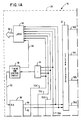
- keyboard apparatus 10 including a keyboard 12 connected by a cable 14 to control circuitry 16 which is adapted to provide a signal representing an actuated key in the keyboard 12.
- the keyboard apparatus 10 is a customer identification module (CIM) which is utilized as part of a data entry unit (not shown) for use with an EFTPOS system or an ATM system. It should be understood that a customer identifies himself to the system by entering his PIN in the keyboard of the CIM. it is highly desirable that the customer PIN remains a secret known only to the customer since unauthorized use of a customer PIN could compromise the system.
- CIM customer identification module
- the possibility of identifying actuated keys by tapping the cable 14 or the row and column conductors within the keyboard 12, is substantially obviated.
- the keyboard 12 includes a conventional key switch array 18 of key switches K0-K15 arranged in rows and columns. Although sixteen key switches K0-K15 arranged in four rows R0-R3 and four columns C0-C3 are shown, it will be appreciated that in other applications a different number of key switches arranged in different numbers of rows and columns could be utilized. In the present embodiment, however, the key switches K0-K15 are connected between four row conductors 20a to 20d and four column conductors 22a to 22d. The row and column conductors 20a to 20d and 22a to 22d are connected to terminals 24a to 24h of the keyboard 12.
- the keyboard terminals 24a-24h are coupled to eight individual conductors 14a to 14h, forming the cable 14.
- the other ends of the eight conductors 14a to 14h are coupled to terminals 26a to 26h of a tamper-resistant module 28.
- a tamper-resistant module is a box-like device which is extremely difficult to penetrate in a manner which can enable the circuitry within the module to be sensed or interfered with.
- An example of a tamper-resistant module is a security module such as is disclosed in U.S. Patent No. 4,593,384.
- the keyboard 12, cable 14 and tamper-resistant module 28 are all located within the CIM containing the keyboard apparatus 10.
- the control circuitry 16 within the tamper-resistant module 28 includes a 6-bit random pattern generator 30, a column decoder 32, a latch 34 and a timing and control circuit 36.
- the random pattern generator 30 has six output lines 40, 42, 44, 46, 48 and 50 and is effective to generate, at a rate of approximately 1000 patterns per second, sequences of random binary bit patterns on the output lines 40-50, such that in a complete cycle of operation of the random pattern generator 30, all possible 6-bit binary patterns are generated in a random order.
- the random patterns are generated in response to clock signals applied over an input line 52 from a clock generator (not shown) included in the timing and control circuit 36.
- the output lines 40 and 42 of the random pattern generator 30, are connected to the column decoder 32 and to the latch 34.
- the output lines 44, 46, 48, 50 are connected to respective row port circuits 54a to 54d and to first inputs of respective EXCLUSIVE-OR gates 56a to 56d.
- the row port circuit 54a includes an inverter 60a having an input connected to the line 44 and an output connected to the gate electrode of an n-channel FET (field effect transistor) 62a having its source electrode connected to ground and its drain electrode connected to a line 64a which is also connected to the terminal 26a of the tamper-resistant module 28 and to one terminal of a resistor 66a, the other terminal of which is connected to a +5V power supply.
- the line 64a is further connected to the input of a buffer circuit 68a, the output of which is connected over a line 70a to a second input of the EXCLUSIVE-OR gate 56a.
- the row port circuits 54b to 54d are of identical construction to the row port circuit 54a, and have correspondingly referenced components included therein. Output lines 70b to 70d of the row port circuits 54b to 54d are connected to respective second inputs of the EXCLUSIVE-OR gates 56b to 56d.
- Output lines 72a to 72d of the EXCLUSIVE-OR gates 56a to 56d are connected to inputs of an OR gate 74 and to inputs of the latch 34.
- the column decoder 32 has four output lines 78a to 78d which are connected to respective column port circuits 80a to 80d.
- the column port circuit 80a includes an inverter 82a having an input connected to the line 78a and an output connected to the gate electrode of an n-channel FET 84a.
- the source electrode of the FET 84a is connected to ground and the drain electrode is connected to a line 86a which is connected to one terminal of a resistor 88a, the other terminal of which is connected to the +5V power supply.
- the line 86a is further connected to the terminal 26e of the tamper-resistant module 28.
- the remaining column port circuits 80b, 80c and 80d are of identical construction to the column port circuit 80a, and have correspondingly referenced components included therein.
- the latch 34 has, in addition to the inputs connected to the lines 40, 42 and 72a to 72d, a further input connected via a line 90 to an output of the timing and control circuit 36.
- the latch 34 also has an output bus 92 on which is provided a signal representing an actuated key in the keyboard 12.
- the keyboard apparatus 10 will now be described. It will be assumed by way of example that the keyboard key switch K8, located in row R2 and column C0 is actuated (closed). As mentioned above, the random pattern generator 30 generates successive binary bit patterns. Assume by way of example, that the bit pattern 000110 is generated on lines 40, 42, 44, 46, 48 and 50, respectively. It should be understood that binary "0" corresponds to a low logic level (0V in the present embodiment) and binary "1" corresponds to a high voltage level (+5V in the present embodiment).
- the binary bits 00 applied over the lines 40 and 42 to the column decoder 32 cause a low level signal to be applied to the output line 78a and high level signals to be applied to the output lines 78b to 78d, thereby rendering the transistor 84a conducting and the transistors 84b to 84d non-conducting.
- This causes a low level signal to be applied to the column conductor 22a and high level signals to be applied to the column conductor 22b to 22d.
- the column C0 is selected when the random pattern generator 30 generates the bit pair 00 on its output lines 40 and 42.
- generated 01, 10 and 11 bit pairs result in the selection of the columns C1, C2 and C3, respectively.
- binary signals corresponding to a binary pattern 0110 are applied to the output lines 44, 46, 48 and 50, respectively, such signals rendering transistors 62a and 62d conducting and transistors 62b and 62c non-conducting.
- low level signals are applied to row conductors 20a and 20d of rows R0 and R3.
- row R2 although the transistor 62c is non-conducting, the presence of the actuated key switch K8 connects the row conductor 20c to the column conductor 22a and, since the transistor 84a is conducting, causes a low level signal to be applied to the row conductor 20c.
- the identification of the genuinely actuated key switch K8 is detected using the EXCLUSIVE-OR gates 56a to 56d located within the tamper-resistant module 28.
- the EXCLUSIVE-OR gates 56a to 56d have binary signals 00, 11, 10 and 00 applied to their respective inputs, whereby only the gate 56c produces an output signal, on its output line 72c.
- the signal on the output line 72c is applied via the OR gate 74 to the timing and control circuit 36, which responds by supplying a latch control signal over the line 90 to the latch 34 thereby latching the signals on the lines 40, 42 and 72a to 72d into the latch 34.
- the binary pattern 000010 is latched, the first two bits identifying the column C0 and the last four bits identifying the row R2.
- data corresponding to the genuinely actuated key switch K8 in row R2 and column C0 is latched into the latch 34 and available on the latch output bus 92.
- the random pattern generator 30 Since the random pattern generator 30 generates random patterns at a high rate, such as 1000 per second, a genuine key entry is effectively "hidden” since the very high proportion of simulated key entries renders the ascertainment of a genuine key entry extremely difficult, and indeed substantially impossible for persons of limited technical knowledge, such as shop personnel, sales clerks or the like. It is found that if random patterns are generated at the aforementioned rate of 1000 patterns per second, then key actuations, including both genuine and simulated key actuations, are generated at the rate of approximately 2000 per second.
- the row and column port circuits 54a to 54d and 80a to 80d are constructed using open-collector type outputs with pull-up resistors 66a to 66d and 88a to 88d.
- the minimum pull-up resistor value should be approximately 50 Kohm to prevent currents and voltage drop levels which might be detectable. The higher the value of the pull-up resistors, the lower the current and hence the more difficult is the detection of currents and voltage drops caused by the difference between a genuine key actuation and a simulated key actuation.
- the voltage difference between a simulated and a genuine key actuation is less than abut 10 milivolts, depending on the parameters of the field effect transistors.
- the row and column port circuits 54a to 54d and 80a to 80d are modified by omitting the pull-up resistors and utilizing additional transistors and associated control circuitry.
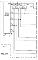
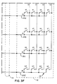
- Parts and components in Figs. 3A to 3F which correspond to parts and components in Figs. 1A to 1D have been given references differing by the value 100, from those of Figs. 1A to 1D.
- the keyboard 112 which includes a key switch array 118 is connected by a cable 114 to control circuitry 116 located within a tamper-resistant module 128.
- the second embodiment will best be understood by directing attention to features which differ from those of the first embodiment.
- the row port circuits 202a to 202d, Fig. 3E differ to some extent from the row port circuits 54a to 54d, Fig. 1B, and the column port 204a to 204d in Fig. 3B differ to some extent from the column port circuits 80a to 80d in Fig. 1B.
- the random pattern generator 130 has a strobe output connected to an output line 206.
- the strobe output supplies a short duration pulse, having a duration of approximately 50 nanoseconds, immediately prior to each new random pattern supplied by the random pattern generator 130.
- the output line 206 is connected to OR gates 208a to 208d and inverters 210a to 120d in the respective row port circuits 202a to 202d, the outputs of the inverters 210a to 210d being connected to the gate electrodes of respective p-channel transistors 212a to 212d.
- the source electrodes of the transistor 212a to 212d are connected to the +5V voltage supply and the drain electrodes are connected to the lines 164a to 164d, respectively.
- the output line 206 is further connected to OR gates 214a to 214d and inverters 216a to 216d in the respective column port circuits 204a to 204d, the outputs of the inverters 216a to 216d being connected to the gate electrodes of respective p-channel transistors 218a to 218d.
- the source electrodes of the transistors 218a to 218d are connected to the +5V voltage supply and the drain electrodes are connected to the lines 186a to 186d respectively.
- the strobe pulse on the line 206 is effective to render the transistors 162a to 162d and 184a to 184d non-conducting and the transistors 212a to 212d and 218a to 218d conducting, thereby charging the inherent capacitances of the row and column conductors 120a to 120d and 122a to 122d.
- the pattern supplied by the random pattern generator 130 is effective to apply a low level logic signal to one of the column conductors 122a to 122d and a random number of the row conductors 120a to 120d, as in the first embodiment.
- the remaining row and column conductors to which high logic level signals were applied during the period of the strobe pulse, will remain high for a period dependent on the capacitance values of the row and column conductors. In the preferred embodiment, this period is in the range of approximately 100 to 500 nanoseconds.
- the EXCLUSIVE-OR gates 156a to 156d and the OR gate 174 are operative to cause the timing and control circuit 136 to provide a latch control signal over the line 190, thereby latching the binary representation of the actuated key switch in the key switch array 118 into the latch 134 for provision on the latch output bus 192.
- the current and voltage levels are the same for a simulated key activation as for a genuine key actuation, and hence a genuine key actuation cannot be distinguished from a simulated key actuation on the basis of a current or voltage level difference.
Landscapes
- Physics & Mathematics (AREA)
- General Physics & Mathematics (AREA)
- Engineering & Computer Science (AREA)
- Computer Security & Cryptography (AREA)
- Theoretical Computer Science (AREA)
- Input From Keyboards Or The Like (AREA)
- Storage Device Security (AREA)
Claims (6)
- Un appareil clavier d'entrée des données, comportant un ensemble de commutateurs à touche (18, 118) connectés entre des conducteurs de ligne et de colonne (20a-20d, 22a-22d; 120a-120d, 122a-122d), et un moyen de commande associé (16, 116) connecté auxdits conducteurs de ligne et de colonne (20a-20d, 22a-22d; 120a-120d, 122a-122d) pour détecter l'actionnement d'un commutateur à touche et fournir un signal de sortie représentant un commutateur à touche actionné, caractérisé en ce que ledit moyen de commande (16, 116) comporte: un moyen de génération de séquences aléatoires (30, 130) adapté pour générer des séquences aléatoires successives de signaux binaires de première et deuxième valeurs; une pluralité de premiers moyens circuits logiques (54a-54d; 202a-202d) couplés à une pluralité de premières sorties (44, 46, 48, 50; 144, 146, 148, 150) dudit moyen de génération de séquences aléatoires (30, 130) et aux sorties respectives desdits conducteurs de ligne (20a-20d; 120a-120d), un moyen de décodage (32, 132) couplé à une pluralité de deuxièmes sorties (40, 42; 140, 142) dudit moyen de génération de séquences aléatoires (30, 130) et à une pluralité de deuxièmes moyens circuits logiques (80a-80d; 204a-204d) couplés respectivement auxdits conducteurs de colonne (22a-22d; 122a-122d), et une pluralité de moyens de détection (56a-56d; 156a-156d) respectivement couplés à ladite pluralité de premières sorties (44, 46, 48, 50; 144, 146, 148, 150) dudit moyen de génération de séquences aléatoires (30, 130) et aux sorties respectives de ladite pluralité de premiers moyens circuits logiques (54a-54d; 202a-202d), selon lequel, en service, chaque séquence aléatoire générée fait fonctionner ledit moyen de décodage (32, 132) pour faire en sorte que lesdits deuxièmes moyens circuits logiques (80a-80d; 204a-204d) fournissent un signal binaire d'une première valeur à un conducteur sélectionné entre lesdits conducteurs de colonne ( 22a-22d; 122a-122d) en fonction de la séquence binaire appliquée par lesdites deuxièmes sorties (40, 42; 140, 142) audit moyen de décodage (32, 132) et un signal binaire d'une deuxième valeur à tous les autres conducteurs de colonne (22a-22d; 122a-122d), et fait fonctionner ladite pluralité de premiers moyens circuits logiques (54a-54d; 202a-202d) en fonction de la séquence binaire appliquée par lesdites premières sorties (44, 46, 48, 50; 144, 146, 148, 150), de façon à ce qu'un conducteur de ligne associé à un commutateur à touche actionné dans la colonne sélectionnée se voie appliquer un signal binaire d'une première valeur, tandis que tous les autres conducteurs de ligne (20a-20d; 120a-120d) se voient appliquer des signaux binaires, correspondant à la séquence aléatoire générée sur lesdites premières sorties (44, 46, 48, 50; 144, 146, 148, 150); et en ce que ladite pluralité de moyens de détection (56a-56d; 156a-156d) est adaptée pour détecter ce premier moyen circuit logique (54a-54d; 202a-202d) qui se voie appliquer un signal binaire d'une deuxième valeur par la séquence aléatoire générée et qui est couplé à un conducteur de ligne comportant un signal binaire d'une première valeur, permettant ainsi la fourniture dudit signal de sortie représentant le commutateur à touche actionné.
- Un appareil clavier d'entrée des données conformément à la revendication 1, caractérisé en ce que ladite pluralité de moyens de détection comporte une pluralité de portes OU EXCLUSIF (56a-56d; 156a-156d) ayant des entrées couplées respectivement auxdites premières sorties (44, 46, 48, 50) dudit moyen de génération de séquences aléatoires (30, 130) et aux sorties dudit premier moyen circuit logique (54a-54d; 202a-202d).
- Un appareil clavier d'entrée des données conformément à la revendication 2, caractérisé en ce que les portes OU EXCLUSIF (56a-56d; 156a-156d) ont des sorties couplées au moyen bascule de maintien (34, 134) et à une porte OU (74, 174), et en ce que lesdites deuxièmes sorties (40, 42; 140, 142) dudit moyen de génération de séquences aléatoires (30, 130) sont couplées audit moyen bascule de maintien (34, 134), ladite porte OU (74, 174) ayant une sortie adaptée pour permettre la fourniture d'un signal de commande de maintien servant à permettre audit moyen bascule de maintien (34, 134) de maintenir les signaux qui lui sont appliqués.
- Un appareil clavier d'entrée des données conformément à la revendication 3, caractérisé en ce que chacun desdits premiers moyens circuits logiques (54a) comporte: un premier transistor à effet de champ (62a) ayant une électrode de grille couplée par l'intermédiaire d'un montage d' inversion (60a) à la première sortie associée (44) dudit moyen de génération de séquences aléatoires (30) et une voie source-drain connectée entre une ligne d'interface de ligne (64a) et un potentiel de référence; et une première résistance (66a) couplée entre un potentiel d'alimentation et ladite ligne d'interface de ligne (64a), ladite ligne d'interface de ligne (64a) étant couplée au conducteur de ligne associé (20a) et à la porte OU EXCLUSIF respective (56a), et en ce que chaque deuxième moyen circuit logique (80a; 80d) comporte: un deuxième transistor à effet de champ (84a) ayant une électrode de grille couplée par l'intermédiaire d'un montage d'inversion (82a) à la sortie associée dudit moyen de décodage (32) et une voie source-drain connectée entre une ligne d'interface de colonne (86a) et un potentiel de référence; et une deuxième résistance (88a) connectée entre ledit potentiel d'alimentation et ladite ligne d'interface de colonne (86a), ladite ligne d'interface de colonne étant couplée au conducteur de colonne associé (22a).
- Un appareil clavier d'entrée des données conformément à la revendication 3, caractérisé en ce que lesdits conducteurs de ligne et de colonne (120a-120d; 122a-122d) ont un moyen capacité respectif qui leur est associé; en ce que ledit premier moyen circuit logique (202a-202d) et ledit deuxième moyen circuit logique (204a-204d) comportent un moyen de chargement respectif (212a-212d; 218a-218d) adapté pour charger le moyen capacité associé, et en ce que ledit moyen de génération de séquences aléatoires (130) est adapté pour fournir un signal de marquage qui sert à faire en sorte que ledit moyen de chargement (212a-212d; 218a-218d) charge ledit moyen capacité avant chaque génération d'une séquence aléatoire.
- Un appareil clavier d'entrée des données conformément à l'une quelconque des revendications précédentes, caractérisé en ce que ledit moyen de commande (16, 116) est logé à l'intérieur d'un module inviolable (28, 128).
Applications Claiming Priority (2)
| Application Number | Priority Date | Filing Date | Title |
|---|---|---|---|
| GB8826340 | 1988-11-10 | ||
| GB888826340A GB8826340D0 (en) | 1988-11-10 | 1988-11-10 | Data entry keyboard apparatus |
Publications (3)
| Publication Number | Publication Date |
|---|---|
| EP0368520A2 EP0368520A2 (fr) | 1990-05-16 |
| EP0368520A3 EP0368520A3 (fr) | 1991-01-02 |
| EP0368520B1 true EP0368520B1 (fr) | 1994-04-20 |
Family
ID=10646657
Family Applications (1)
| Application Number | Title | Priority Date | Filing Date |
|---|---|---|---|
| EP89311114A Expired - Lifetime EP0368520B1 (fr) | 1988-11-10 | 1989-10-27 | Dispositif d'entrée de données réalisé sous forme de clavier |
Country Status (4)
| Country | Link |
|---|---|
| US (1) | US4926173A (fr) |
| EP (1) | EP0368520B1 (fr) |
| DE (1) | DE68914782T2 (fr) |
| GB (1) | GB8826340D0 (fr) |
Families Citing this family (28)
| Publication number | Priority date | Publication date | Assignee | Title |
|---|---|---|---|---|
| GB2223115B (en) * | 1988-09-22 | 1992-02-05 | Bollmann Limited H | Improvements in or relating to a keyboard arrangement |
| US5254989A (en) * | 1988-12-20 | 1993-10-19 | Bull S.A. | Garbling the identification of a key of a non-coded keyboard, and circuit for performing the method |
| EP0476283B1 (fr) * | 1990-09-17 | 1996-02-07 | Siemens Nixdorf Informationssysteme Aktiengesellschaft | Procédé de masquage de donnée à l'aide d'un clavier pour des données de sécurité |
| FR2692378B1 (fr) * | 1992-06-12 | 1994-07-29 | Dassault Automatismes Telecomm | Unite a clavier de securite perfectionnee. |
| FR2723806A1 (fr) * | 1994-08-17 | 1996-02-23 | Schlumberger Ind Sa | Dispositif de clavier securise |
| US5521986A (en) * | 1994-11-30 | 1996-05-28 | American Tel-A-Systems, Inc. | Compact data input device |
| US5754652A (en) * | 1994-12-14 | 1998-05-19 | Lucent Technologies Inc. | Method and apparatus for secure pin entry |
| US5832206A (en) * | 1996-03-25 | 1998-11-03 | Schlumberger Technologies, Inc. | Apparatus and method to provide security for a keypad processor of a transaction terminal |
| FI102119B1 (fi) * | 1996-10-04 | 1998-10-15 | Nokia Mobile Phones Ltd | Näppäimistöjärjestely ja menetelmä painetun näppäimen tunnistamiseksi |
| US5987439A (en) * | 1997-05-30 | 1999-11-16 | Capital Security Systems, Inc. | Automated banking system for making change on a card or user account |
| JP2002502531A (ja) * | 1997-05-30 | 2002-01-22 | キャピタル セキュリティー システムズ インコーポレイション | 自動書類キャッシングシステム |
| US6012048A (en) * | 1997-05-30 | 2000-01-04 | Capital Security Systems, Inc. | Automated banking system for dispensing money orders, wire transfer and bill payment |
| US5897625A (en) * | 1997-05-30 | 1999-04-27 | Capital Security Systems, Inc. | Automated document cashing system |
| US7653600B2 (en) * | 1997-05-30 | 2010-01-26 | Capital Security Systems, Inc. | Automated document cashing system |
| US7249109B1 (en) * | 1997-07-15 | 2007-07-24 | Silverbrook Research Pty Ltd | Shielding manipulations of secret data |
| US7249108B1 (en) * | 1997-07-15 | 2007-07-24 | Silverbrook Research Pty Ltd | Validation protocol and system |
| US7246098B1 (en) * | 1997-07-15 | 2007-07-17 | Silverbrook Research Pty Ltd | Consumable authentication protocol and system |
| US7743262B2 (en) * | 1997-07-15 | 2010-06-22 | Silverbrook Research Pty Ltd | Integrated circuit incorporating protection from power supply attacks |
| US6054940A (en) * | 1998-02-09 | 2000-04-25 | Gilbarco Inc. | Keypad scanning security system |
| US6816968B1 (en) * | 1998-07-10 | 2004-11-09 | Silverbrook Research Pty Ltd | Consumable authentication protocol and system |
| TW376499B (en) * | 1998-12-17 | 1999-12-11 | Xac Automation Corp | A method for detecting a keyboard key through two corresponding lines separately belonging to X port and Y port lines when each key is pressed down |
| US6578145B1 (en) | 1999-06-29 | 2003-06-10 | Gilbarco Inc. | Methods and systems for securely communicating personal identification number information between a security module and a plurality of secure keypad devices |
| AUPQ673400A0 (en) * | 2000-04-06 | 2000-05-04 | Mcom Solutions Inc | Keypad |
| AU2001239012B2 (en) * | 2001-03-16 | 2005-12-01 | Mcom Solutions Inc | Keypad |
| US7181767B1 (en) * | 2001-05-08 | 2007-02-20 | Nxp B.V. | Keypad device security system and method |
| KR100378586B1 (ko) * | 2001-08-29 | 2003-04-03 | 테커스 (주) | 엑티브엑스 기반의 키보드 해킹 방지 방법 및 장치 |
| EP1548947B1 (fr) | 2003-12-22 | 2007-03-28 | Banksys S.A. | Procédé et dispositif pour lire des touches de clavier |
| US8081091B2 (en) * | 2008-07-31 | 2011-12-20 | Maxim Integrated Products, Inc. | Secure keypad scanning |
Family Cites Families (7)
| Publication number | Priority date | Publication date | Assignee | Title |
|---|---|---|---|---|
| US4479112A (en) * | 1980-05-05 | 1984-10-23 | Secure Keyboards Limited | Secure input system |
| JPS58161026A (ja) * | 1982-03-19 | 1983-09-24 | Hitachi Ltd | 入力装置 |
| EP0094130B1 (fr) * | 1982-05-07 | 1987-01-21 | Philips Electronics Uk Limited | Dispositif de clavier pour l'introduction de données |
| US4617554A (en) * | 1983-08-26 | 1986-10-14 | Zenith Electronics Corporation | Keyboard scanning |
| US4549094A (en) * | 1983-10-07 | 1985-10-22 | United Technologies Automotive, Inc. | Debounce circuit providing synchronously clocked digital signals |
| SE448803B (sv) * | 1986-05-22 | 1987-03-16 | Ljungmans Ind Ab | Sett att forhindra obehorig atkomst av information |
| FR2599525B1 (fr) * | 1986-06-02 | 1988-07-29 | Dassault Electronique | Unite a clavier de securite, en particulier pour la composition d'un code confidentiel |
-
1988
- 1988-11-10 GB GB888826340A patent/GB8826340D0/en active Pending
-
1989
- 1989-04-03 US US07/331,767 patent/US4926173A/en not_active Expired - Fee Related
- 1989-10-27 EP EP89311114A patent/EP0368520B1/fr not_active Expired - Lifetime
- 1989-10-27 DE DE68914782T patent/DE68914782T2/de not_active Expired - Fee Related
Also Published As
| Publication number | Publication date |
|---|---|
| EP0368520A2 (fr) | 1990-05-16 |
| US4926173A (en) | 1990-05-15 |
| DE68914782D1 (de) | 1994-05-26 |
| GB8826340D0 (en) | 1988-12-14 |
| DE68914782T2 (de) | 1994-11-24 |
| EP0368520A3 (fr) | 1991-01-02 |
Similar Documents
| Publication | Publication Date | Title |
|---|---|---|
| EP0368520B1 (fr) | Dispositif d'entrée de données réalisé sous forme de clavier | |
| US5832206A (en) | Apparatus and method to provide security for a keypad processor of a transaction terminal | |
| US6710269B2 (en) | Foil keyboard with security system | |
| EP0046763B1 (fr) | Appareil de sécurite à touches | |
| US4064560A (en) | Master keyboard terminal with auxiliary keyboard terminal capability | |
| US4525599A (en) | Software protection methods and apparatus | |
| EP2919210B1 (fr) | Procédé de protection destiné à des informations de données relatives à un dispositif électronique et circuit de protection associé | |
| US6279825B1 (en) | Electronic transaction terminal for preventing theft of sensitive information | |
| US3786497A (en) | Matrix keyboard method and apparatus | |
| US4103289A (en) | Calculator theft prevention device | |
| HK80897A (en) | Method for verifying the integrity of software or data and system for implementing this method | |
| GB2120434A (en) | A security system | |
| FI117216B (fi) | Suojattu näppäimistölaite | |
| US7290151B2 (en) | Logic circuit with variable internal polarities | |
| EP0272230B1 (fr) | Pupitre d'opérateur pour usage en communication de données | |
| CA1293039C (fr) | Appareil de saisie de donnees a clavier | |
| JP2838418B2 (ja) | データ・エントリ・キーボード装置 | |
| US4232291A (en) | Electronic lock, the code of which can easily be modified by the user | |
| KR100718352B1 (ko) | 데이터 처리 장치 및 그 작동 방법 | |
| FI85637B (fi) | Saett att foerhindra obehoerig aotkomst av information. | |
| US8081091B2 (en) | Secure keypad scanning | |
| WO2001077801A1 (fr) | Clavier | |
| KR19980052634A (ko) | 키패드용 숫자의 무작위 조합장치 | |
| US3648021A (en) | Electronic validator system for magnetic credit cards and the like | |
| IL33602A (en) | Coded switching device using random numbers |
Legal Events
| Date | Code | Title | Description |
|---|---|---|---|
| PUAI | Public reference made under article 153(3) epc to a published international application that has entered the european phase |
Free format text: ORIGINAL CODE: 0009012 |
|
| AK | Designated contracting states |
Kind code of ref document: A2 Designated state(s): DE FR GB |
|
| PUAL | Search report despatched |
Free format text: ORIGINAL CODE: 0009013 |
|
| AK | Designated contracting states |
Kind code of ref document: A3 Designated state(s): DE FR GB |
|
| 17P | Request for examination filed |
Effective date: 19910622 |
|
| 17Q | First examination report despatched |
Effective date: 19930429 |
|
| RAP1 | Party data changed (applicant data changed or rights of an application transferred) |
Owner name: NCR INTERNATIONAL INC. |
|
| GRAA | (expected) grant |
Free format text: ORIGINAL CODE: 0009210 |
|
| AK | Designated contracting states |
Kind code of ref document: B1 Designated state(s): DE FR GB |
|
| REF | Corresponds to: |
Ref document number: 68914782 Country of ref document: DE Date of ref document: 19940526 |
|
| ET | Fr: translation filed | ||
| PLBE | No opposition filed within time limit |
Free format text: ORIGINAL CODE: 0009261 |
|
| STAA | Information on the status of an ep patent application or granted ep patent |
Free format text: STATUS: NO OPPOSITION FILED WITHIN TIME LIMIT |
|
| 26N | No opposition filed | ||
| REG | Reference to a national code |
Ref country code: GB Ref legal event code: IF02 |
|
| PGFP | Annual fee paid to national office [announced via postgrant information from national office to epo] |
Ref country code: GB Payment date: 20021003 Year of fee payment: 14 |
|
| PGFP | Annual fee paid to national office [announced via postgrant information from national office to epo] |
Ref country code: FR Payment date: 20021029 Year of fee payment: 14 |
|
| PGFP | Annual fee paid to national office [announced via postgrant information from national office to epo] |
Ref country code: DE Payment date: 20021209 Year of fee payment: 14 |
|
| PG25 | Lapsed in a contracting state [announced via postgrant information from national office to epo] |
Ref country code: GB Free format text: LAPSE BECAUSE OF NON-PAYMENT OF DUE FEES Effective date: 20031027 |
|
| PG25 | Lapsed in a contracting state [announced via postgrant information from national office to epo] |
Ref country code: DE Free format text: LAPSE BECAUSE OF NON-PAYMENT OF DUE FEES Effective date: 20040501 |
|
| GBPC | Gb: european patent ceased through non-payment of renewal fee |
Effective date: 20031027 |
|
| PG25 | Lapsed in a contracting state [announced via postgrant information from national office to epo] |
Ref country code: FR Free format text: LAPSE BECAUSE OF NON-PAYMENT OF DUE FEES Effective date: 20040630 |
|
| REG | Reference to a national code |
Ref country code: FR Ref legal event code: ST |