EP0368524A1 - Output buffer circuit - Google Patents
Output buffer circuit Download PDFInfo
- Publication number
- EP0368524A1 EP0368524A1 EP89311147A EP89311147A EP0368524A1 EP 0368524 A1 EP0368524 A1 EP 0368524A1 EP 89311147 A EP89311147 A EP 89311147A EP 89311147 A EP89311147 A EP 89311147A EP 0368524 A1 EP0368524 A1 EP 0368524A1
- Authority
- EP
- European Patent Office
- Prior art keywords
- transistor
- output
- buffer circuit
- power supply
- pad
- Prior art date
- Legal status (The legal status is an assumption and is not a legal conclusion. Google has not performed a legal analysis and makes no representation as to the accuracy of the status listed.)
- Granted
Links
- 239000000872 buffer Substances 0.000 title claims abstract description 20
- 230000000295 complement effect Effects 0.000 claims description 5
- 230000005669 field effect Effects 0.000 claims description 5
- 239000003990 capacitor Substances 0.000 abstract description 10
- 230000008859 change Effects 0.000 abstract description 5
- 230000004044 response Effects 0.000 abstract description 3
- 230000007704 transition Effects 0.000 description 9
- 230000000694 effects Effects 0.000 description 6
- 230000000875 corresponding effect Effects 0.000 description 5
- 230000008901 benefit Effects 0.000 description 2
- 230000009471 action Effects 0.000 description 1
- 230000002301 combined effect Effects 0.000 description 1
- 230000007423 decrease Effects 0.000 description 1
- 230000003247 decreasing effect Effects 0.000 description 1
- 238000011161 development Methods 0.000 description 1
- 230000018109 developmental process Effects 0.000 description 1
- 238000011835 investigation Methods 0.000 description 1
- 238000004519 manufacturing process Methods 0.000 description 1
- 238000000034 method Methods 0.000 description 1
- 230000008569 process Effects 0.000 description 1
- 230000000750 progressive effect Effects 0.000 description 1
- 230000000630 rising effect Effects 0.000 description 1
- 230000035945 sensitivity Effects 0.000 description 1
- 238000007493 shaping process Methods 0.000 description 1
- 230000001052 transient effect Effects 0.000 description 1
Images

Classifications
-
- G—PHYSICS
- G11—INFORMATION STORAGE
- G11C—STATIC STORES
- G11C7/00—Arrangements for writing information into, or reading information out from, a digital store
- G11C7/10—Input/output [I/O] data interface arrangements, e.g. I/O data control circuits, I/O data buffers
- G11C7/1051—Data output circuits, e.g. read-out amplifiers, data output buffers, data output registers, data output level conversion circuits
-
- G—PHYSICS
- G11—INFORMATION STORAGE
- G11C—STATIC STORES
- G11C7/00—Arrangements for writing information into, or reading information out from, a digital store
- G11C7/10—Input/output [I/O] data interface arrangements, e.g. I/O data control circuits, I/O data buffers
- G11C7/1078—Data input circuits, e.g. write amplifiers, data input buffers, data input registers, data input level conversion circuits
-
- H—ELECTRICITY
- H03—ELECTRONIC CIRCUITRY
- H03K—PULSE TECHNIQUE
- H03K19/00—Logic circuits, i.e. having at least two inputs acting on one output; Inverting circuits
- H03K19/003—Modifications for increasing the reliability for protection
- H03K19/00346—Modifications for eliminating interference or parasitic voltages or currents
- H03K19/00361—Modifications for eliminating interference or parasitic voltages or currents in field effect transistor circuits
-
- H—ELECTRICITY
- H03—ELECTRONIC CIRCUITRY
- H03K—PULSE TECHNIQUE
- H03K19/00—Logic circuits, i.e. having at least two inputs acting on one output; Inverting circuits
- H03K19/02—Logic circuits, i.e. having at least two inputs acting on one output; Inverting circuits using specified components
- H03K19/08—Logic circuits, i.e. having at least two inputs acting on one output; Inverting circuits using specified components using semiconductor devices
- H03K19/094—Logic circuits, i.e. having at least two inputs acting on one output; Inverting circuits using specified components using semiconductor devices using field-effect transistors
- H03K19/09425—Multistate logic
- H03K19/09429—Multistate logic one of the states being the high impedance or floating state
Definitions
- This invention relates to output buffer circuits suitable for use in an integrated circuit chip.
- CMOS type integrated circuits in that CMOS integrated circuit loads are predominately capacitive.
- an output buffer circuit for an integrated circuit, characterized by: an output node, driven by a first transistor connected to a first side of a power supply; capacitive feedback means connected between said output node and a control electrode of said first transistor; a second transistor connected between said control electrode of said first transistor and said first side of said power supply to relatively rapidly pull said control electrode of said first transistor to the potential of said first side of the power supply responsive to a DATA IN signal first state; and switch means connected between a second side of said power supply to slowly pull said control electrode of said first transistor toward a second side of said power supply responsive to a DATA IN signal second state.
- An output buffer circuit has the advantage of adjusting the rate of change of the output buffer current in relation to the magnitude of the capacitive load on the output pad, limiting rapid current changes and thereby constraining associated power supply and ground line di/dt noise levels, and ensuring full pull-up of the output stage following transition.
- the combination of these advantages provides load responsive feedback sensitivity, reduces current surge noise, and ensures concluding DC voltage levels of appropriate magnitudes.
- the invention as preferably embodied incorporates capacitive feedback between the output node and the control electrode of the output transistor to adjust the switching rate of the output transistor in relation to the capacitive load.
- the turn-on current spike in the output transistor is further controlled by a resistive element interposed between the output transistor control gate and the switched source of the control signal.
- the steady-state voltage on the output node is established using a pull-up transistor driven by a logic gate output signal. The output state of such logic gate is based upon the combination of the input command signal and the level of the output node voltage in its progression toward the final steady-state level.
- a preferred embodiment of a tri-state configuration using push-pull output transistors includes a pull-down transistor acting upon the control gate of the output transistor.
- the pull-down transistor is designed to switch the control gate of the output transistor significantly faster than the control gate is switched during turn-on. This avoids a switching overlap type of short circuit condition when complementary pairs of transistors are used to drive the output.
- Tri-state operation is enabled through multiple logic gates, which selectively interact with the turn-on and steady-state control signals.
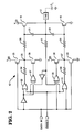
- Buffer circuit 1 in Fig. 1 illustrates in a fundamental form the elements which contribute to the present invention.
- the circuit is particularly suited to drive an output pad of an integrated circuit in response to signals generated within the integrated circuit.
- the schematic in Fig. 1 also includes the output pad 2 and a representative capacitive pad load C L .
- the objective is to accept high switching rate DATA IN signals and have field effect transistor 3 drive the output pad 2 accordingly while minimizing the di/dt effects on the ground line.
- n-channel output driver field effect transistor 3 has a slew rate limiting feedback capacitor 7 connected between its source electrode 4 and its control gate electrode 6.
- Second, pull-up action on node 9 and its progressive effect on control electrode 6 to enable driver transistor 3 is constrained by the limited output capacity of inverter 12. Consequently, the slew rate of rising voltage on the gate electrode 6 which enables transistor 3 is reduced through the combined effects of limited drive inverter 12, resistor 11, resistor 13 and capacitor 7.
- Positive transitioning DATA IN signals are used to directly enable relatively large and fast transistor 8.
- Transistor 8 pulls node 9 and gate electrode 6 of transistor 3 toward ground significantly faster than the rate at which node 9 is able to transition in the positive direction.
- the third aspect of the invention arises from the logical combination of signals entering OR gate 14.
- OR gate 14 combines the DATA IN signal and a feedback signal from pad 2, defining therefrom an output signal to drive p-channel transistor 16.
- OR gate 14 enables transistor 16, to pull node 9 to the supply voltage V DD , after the DATA IN signal is low and the voltage on pad 2 has decreased to approximately half the supply voltage.
- This third aspect of the invention ensures that the concluding or steady state drive to transistor 3 from node 9 is based upon the full voltage of the power supply V DD .
- a nominal value for feedback capacitor 7 is in the range of 2 picofarads for an output transistor 3 which is designed to drive a nominal capacitive load C L of 50 picofarads and to exhibit a nominal DC current conduction capability of 24 milliamps.
- resistors 11 and 13 nominally range from 300 to 400 ohms, while feedback resistor 17 is nominally 250 ohms in value.
- the physical dimensions and electrical characteristics of pull-down transistor 8 should be selected to ensure that the pull-down rate of gate electrode 6 is approximately four times the pull-up rate produced by inverter 12.
- FIG. 2 A preferred and fully implemented arrangement of the invention, as first rudimentally depicted in Fig. 1, appears in Fig. 2.
- the circuit now incorporates a tri-state capability with a selectively operable enable mode responsive to an ENABLE signal.
- output pad 2 is driven by a complementary pair of field effect transistors, with p-channel transistor 18 pulling pad 2 to the power supply node V DD and n-channel transistor 19 pulling pad 2 to ground potential.
- the control or gate electrodes of each of the output pad driver transistors 18 and 19 are coupled through respective feedback capacitors 21 and 22 to the node represented by pad 2.
- the gate electrodes of transistors 18 and 19 are themselves individually driven by electrically complementary pulling transistors 23 and 24, which pulling transistors act upon intermediate nodes 26 and 27 in direct response to the DATA IN signal level. Again, intermediate nodes 26 and 27 are separated from the control gate electrodes of driver transistors 18 and 19 by respective resistors 28 and 29.
- resistors 33 and 34 separate respective logic gates 31 and 32 from intermediate nodes 27 and 26 to establish a relative difference in the rate of change of the control gate voltages on the driver transistors 18 and 19 depending on whether the input signal transition is high-to-low or low-to-high.
- transistors 23 and 24 disable their respective output driver transistors 18 and 19 approximately four times faster than the enablement effectuated by respective gates 37 and 36 to eliminate inadvertent and undesirable simultaneous enablements of both transistors 18 and 19. This factor of four is believed to provide a sufficient margin, between the disablement of one output driver transistor and the enablement of its complement transistor, to offset performance differences attributable to normal fabrication process variations.
- the steady-state signals on output pad 2 are again guaranteed appropriate by logic gates sensing the state of the output pad voltage.
- OR gate 36 and NOR gate 37 acting respectively on p-channel transistor 38 and n-channel transistor 39 to fully pull the respective intermediate nodes 27 and 26 to the appropriate power supply and ground potential levels for complete enablement of the output driver transistors 19 and 18.
- logic gates 36 and 37 respond to the feedback signal conveyed through resistor 41 from pad 2 when the pad voltage reaches approximately half the power supply voltage.
- a high level signal on the ENABLE/ line places buffer circuit 42 in Fig. 2 into a tri-state mode of operation, whereupon pad 2 is to be simultaneously disconnected from both the power supply and ground lines. This is accomplished by concurrently disabling both the output driver transistors 18 and 19.
- the ENABLE/ state is conveyed to the gates which define the initial rate of rise of current, namely, gates 31 and 32, as well as the gates which establish the steady-state voltages on nodes 27 and 26, namely, gates 36 and 37.
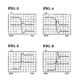
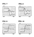
- Figs. 3-10 The ability of the circuit in Fig. 2 to materially reduce ground and power supply line noise spikes attributable to high rates of change of current, di/dt, is evidenced in the succession of performance plots depicted in Figs. 3-10.
- Each of the figures shows a pad output voltage transition of approximately 5 volts and the noise voltage level on the related supply voltage or ground line.
- Figs. 3-6 are waveforms for pads loaded at a nominal level of 20 picofarads, while Figs. 7-10 relate to pads having nominal 120 picofarad loads.
- Fig. 3 The waveforms in Fig. 3 are attributable to a high-to-low voltage transition of the pad voltage for the circuit in Fig. 2, while Fig. 4 is the corresponding transition performance of a relatively comparable prior art output pad driver circuit.
- Fig. 5 illustrates the positive going transition and associated noise for the circuit of the present invention
- Fig. 6 illustrate the corresponding performance of the prior art.
- Fig. 7 illustrates the effects of a larger capacitive load on the circuit of the present invention under the high-to-low transition condition
- Fig. 8 illustrate the effects of the corresponding conditions on the prior art circuit.
- Fig. 9 illustrates the low-to-high transition for the present invention circuit under heavy capacitive load
- Fig. 10 is representative of the prior art performance.
- the 20 picofarad load used for the plots in Figs. 3-6 is attributable to the test oscilloscope, the pad being otherwise unloaded.
- the 120 picofarad loads used for the test results shown in by Figs. 7-10 involved the addition of 100 picofarad passive loads to pad 2.
- the importance of the feedback capacitors 21 and 22 within the circuit of Fig. 2 should not be underestimated. Not only do the capacitors contribute to the shaping of the waveforms during the three increments of operation described in detail hereinbefore, but they provide negative feedback suitable to constrain the switching rates for low levels of capacitive load on the output pad 2. Whereas most prior art developments focus solely on limiting the current flow through the driver transistors for heavy capacitive load conditions, the present circuit extends the range of the control into low capacitive loading ranges with high di/dt effects. All high rates of change of voltage on the pad are fed back through the capacitors 21 or 22 to the gate electrodes of the driver transistors. Consequently, the present circuit provides both open loop and closed loop compensation for variations of capacitive load on the pad, a class of load typical for contemporary and advanced CMOS class integrated circuit devices.
Landscapes
- Engineering & Computer Science (AREA)
- Physics & Mathematics (AREA)
- Computer Hardware Design (AREA)
- Computing Systems (AREA)
- General Engineering & Computer Science (AREA)
- Mathematical Physics (AREA)
- Power Engineering (AREA)
- Electronic Switches (AREA)
- Logic Circuits (AREA)
- Manipulation Of Pulses (AREA)
- Static Random-Access Memory (AREA)
Abstract
Description
- This invention relates to output buffer circuits suitable for use in an integrated circuit chip.
- The voltage spikes which appear as noise on the ground lines and power supply lines of integrated circuit devices have increased both in prevalence and relative magnitude with the evolution toward smaller integrated circuit dimensions. Investigations have established that the resistance and inductance of the interconnect lines within the integrated circuit chip have became major sources of transient noise voltages. Rapid changes of current to and from the power supply and ground pads contribute significantly to the levels of noise on such corresponding lines throughout the chip. Concurrently, decreases in integrated circuit dimensions constrain designers from materially reducing the power supply and ground line impedance levels by expanding line widths. Attempts to eliminate or suppress noise sources are further complicated by the increases in the integrated circuit device switching speeds and their associated di/dt effects.
- Integrated circuit power supply and ground line noise signals attributable to resistance and di/dt effects appear most often when input/output (I/O) buffers are used to switch capacitive loads. The significance of this noise source is expected to increase with the use of more CMOS type integrated circuits, in that CMOS integrated circuit loads are predominately capacitive.
- It is an object of the present invention to provide an output buffer circuit which has a high operating efficiency.
- Therefore, according to the present invention, there is provided an output buffer circuit for an integrated circuit, characterized by: an output node, driven by a first transistor connected to a first side of a power supply; capacitive feedback means connected between said output node and a control electrode of said first transistor; a second transistor connected between said control electrode of said first transistor and said first side of said power supply to relatively rapidly pull said control electrode of said first transistor to the potential of said first side of the power supply responsive to a DATA IN signal first state; and switch means connected between a second side of said power supply to slowly pull said control electrode of said first transistor toward a second side of said power supply responsive to a DATA IN signal second state.
- An output buffer circuit according to the invention has the advantage of adjusting the rate of change of the output buffer current in relation to the magnitude of the capacitive load on the output pad, limiting rapid current changes and thereby constraining associated power supply and ground line di/dt noise levels, and ensuring full pull-up of the output stage following transition. The combination of these advantages provides load responsive feedback sensitivity, reduces current surge noise, and ensures concluding DC voltage levels of appropriate magnitudes.
- The invention as preferably embodied incorporates capacitive feedback between the output node and the control electrode of the output transistor to adjust the switching rate of the output transistor in relation to the capacitive load. The turn-on current spike in the output transistor is further controlled by a resistive element interposed between the output transistor control gate and the switched source of the control signal. The steady-state voltage on the output node is established using a pull-up transistor driven by a logic gate output signal. The output state of such logic gate is based upon the combination of the input command signal and the level of the output node voltage in its progression toward the final steady-state level.
- A preferred embodiment of a tri-state configuration using push-pull output transistors, includes a pull-down transistor acting upon the control gate of the output transistor. The pull-down transistor is designed to switch the control gate of the output transistor significantly faster than the control gate is switched during turn-on. This avoids a switching overlap type of short circuit condition when complementary pairs of transistors are used to drive the output. Tri-state operation is enabled through multiple logic gates, which selectively interact with the turn-on and steady-state control signals.
- Embodiments of the invention will now be described by way of example with reference to the accompanying drawings, in which:-
- Fig. 1 is a circuit schematically illustrating the basic features of the invention.
- Fig. 2 is a schematic showing a preferred embodiment of the invention with CMOS field effect transistors and tri-state control; and
- Figs. 3-10 are plots illustrating the relative performance levels of the preferred embodiment and representative prior art.
-
Buffer circuit 1 in Fig. 1 illustrates in a fundamental form the elements which contribute to the present invention. The circuit is particularly suited to drive an output pad of an integrated circuit in response to signals generated within the integrated circuit. The schematic in Fig. 1 also includes theoutput pad 2 and a representative capacitive pad load CL. In the context of the schematic in Fig. 1, the objective is to accept high switching rate DATA IN signals and havefield effect transistor 3 drive theoutput pad 2 accordingly while minimizing the di/dt effects on the ground line. - The objectives are satisfied through the contribution of three circuit structure arrangements. First, n-channel output driver
field effect transistor 3 has a slew rate limiting feedback capacitor 7 connected between its source electrode 4 and itscontrol gate electrode 6. Second, pull-up action onnode 9 and its progressive effect oncontrol electrode 6 to enabledriver transistor 3 is constrained by the limited output capacity ofinverter 12. Consequently, the slew rate of rising voltage on thegate electrode 6 which enablestransistor 3 is reduced through the combined effects oflimited drive inverter 12,resistor 11,resistor 13 and capacitor 7. Positive transitioning DATA IN signals are used to directly enable relatively large andfast transistor 8.Transistor 8 pullsnode 9 andgate electrode 6 oftransistor 3 toward ground significantly faster than the rate at whichnode 9 is able to transition in the positive direction. The third aspect of the invention arises from the logical combination of signals enteringOR gate 14. ORgate 14 combines the DATA IN signal and a feedback signal frompad 2, defining therefrom an output signal to drive p-channel transistor 16. Preferably, ORgate 14 enablestransistor 16, to pullnode 9 to the supply voltage VDD, after the DATA IN signal is low and the voltage onpad 2 has decreased to approximately half the supply voltage. This third aspect of the invention ensures that the concluding or steady state drive totransistor 3 fromnode 9 is based upon the full voltage of the power supply VDD. - A nominal value for feedback capacitor 7 is in the range of 2 picofarads for an
output transistor 3 which is designed to drive a nominal capacitive load CL of 50 picofarads and to exhibit a nominal DC current conduction capability of 24 milliamps. For these capacities,resistors feedback resistor 17 is nominally 250 ohms in value. The physical dimensions and electrical characteristics of pull-down transistor 8 should be selected to ensure that the pull-down rate ofgate electrode 6 is approximately four times the pull-up rate produced byinverter 12. - A preferred and fully implemented arrangement of the invention, as first rudimentally depicted in Fig. 1, appears in Fig. 2. The circuit now incorporates a tri-state capability with a selectively operable enable mode responsive to an ENABLE signal. To implement the tri-state capability required of the circuit,
output pad 2 is driven by a complementary pair of field effect transistors, with p-channel transistor 18pulling pad 2 to the power supply node VDD and n-channel transistor 19pulling pad 2 to ground potential. The control or gate electrodes of each of the outputpad driver transistors respective feedback capacitors pad 2. The gate electrodes oftransistors complementary pulling transistors intermediate nodes intermediate nodes driver transistors respective resistors - The limited current drive capacity of NOR
gate 31, as further constrained byresistors feedback capacitor 22, together establish the initial slope of the pad-to-ground current conducted by pull-downdriver transistor 19. The current capacity ofOR gate 32, interacting withcapacitor 21 throughresistors up driver transistor 18. - In keeping with the concepts introduced with reference to the structure in Fig. 1,
resistors respective logic gates intermediate nodes driver transistors transistors output driver transistors respective gates transistors - The steady-state signals on
output pad 2 are again guaranteed appropriate by logic gates sensing the state of the output pad voltage. In this embodiment, ORgate 36 andNOR gate 37 acting respectively on p-channel transistor 38 and n-channel transistor 39 to fully pull the respectiveintermediate nodes output driver transistors logic gates resistor 41 frompad 2 when the pad voltage reaches approximately half the power supply voltage. - A high level signal on the ENABLE/ line
places buffer circuit 42 in Fig. 2 into a tri-state mode of operation, whereuponpad 2 is to be simultaneously disconnected from both the power supply and ground lines. This is accomplished by concurrently disabling both theoutput driver transistors gates nodes gates - The ability of the circuit in Fig. 2 to materially reduce ground and power supply line noise spikes attributable to high rates of change of current, di/dt, is evidenced in the succession of performance plots depicted in Figs. 3-10. Each of the figures shows a pad output voltage transition of approximately 5 volts and the noise voltage level on the related supply voltage or ground line. Figs. 3-6 are waveforms for pads loaded at a nominal level of 20 picofarads, while Figs. 7-10 relate to pads having nominal 120 picofarad loads.
- The waveforms in Fig. 3 are attributable to a high-to-low voltage transition of the pad voltage for the circuit in Fig. 2, while Fig. 4 is the corresponding transition performance of a relatively comparable prior art output pad driver circuit. Similarly, Fig. 5 illustrates the positive going transition and associated noise for the circuit of the present invention, while Fig. 6 illustrate the corresponding performance of the prior art. The effects of a larger capacitive load on the circuit of the present invention under the high-to-low transition condition are illustrated in Fig. 7, while the effects of the corresponding conditions on the prior art circuit are shown in Fig. 8. Fig. 9 illustrates the low-to-high transition for the present invention circuit under heavy capacitive load, while Fig. 10 is representative of the prior art performance. A comparison of the noise levels clearly establishes the improved performance exhibited by the present circuit. For instance, a relative 50 millivolts peak-to-peak of noise is exhibited by the present invention in Fig. 3 compared to more than twice that amount for the prior art in Fig. 4.
- The 20 picofarad load used for the plots in Figs. 3-6 is attributable to the test oscilloscope, the pad being otherwise unloaded. The 120 picofarad loads used for the test results shown in by Figs. 7-10 involved the addition of 100 picofarad passive loads to
pad 2. - The importance of the
feedback capacitors output pad 2. Whereas most prior art developments focus solely on limiting the current flow through the driver transistors for heavy capacitive load conditions, the present circuit extends the range of the control into low capacitive loading ranges with high di/dt effects. All high rates of change of voltage on the pad are fed back through thecapacitors
Claims (10)
Applications Claiming Priority (2)
| Application Number | Priority Date | Filing Date | Title |
|---|---|---|---|
| US07/269,022 US4906867A (en) | 1988-11-09 | 1988-11-09 | Buffer circuit with load sensitive transition control |
| US269022 | 2002-10-10 |
Publications (2)
| Publication Number | Publication Date |
|---|---|
| EP0368524A1 true EP0368524A1 (en) | 1990-05-16 |
| EP0368524B1 EP0368524B1 (en) | 1994-01-12 |
Family
ID=23025500
Family Applications (1)
| Application Number | Title | Priority Date | Filing Date |
|---|---|---|---|
| EP89311147A Expired - Lifetime EP0368524B1 (en) | 1988-11-09 | 1989-10-27 | Output buffer circuit |
Country Status (4)
| Country | Link |
|---|---|
| US (1) | US4906867A (en) |
| EP (1) | EP0368524B1 (en) |
| JP (1) | JP2700419B2 (en) |
| DE (1) | DE68912277T2 (en) |
Cited By (15)
| Publication number | Priority date | Publication date | Assignee | Title |
|---|---|---|---|---|
| WO1991020129A1 (en) * | 1990-06-12 | 1991-12-26 | Robert Bosch Gmbh | Circuit for limiting the rate of increase in the signal level of output signals of integrated circuits |
| EP0502597A3 (en) * | 1991-03-07 | 1992-10-21 | Advanced Micro Devices, Inc. | Cmos output buffer circuit |
| EP0533971A1 (en) * | 1991-09-24 | 1993-03-31 | Siemens Aktiengesellschaft | Interface circuit |
| EP0490654A3 (en) * | 1990-12-12 | 1993-08-04 | Texas Instruments Incorporated | Output buffer |
| EP0577367A3 (en) * | 1992-06-30 | 1995-05-17 | Sgs Thomson Microelectronics | Slew rate circuit for high side driver for a polyphase DC motor. |
| WO1995024076A1 (en) * | 1994-03-01 | 1995-09-08 | Apple Computer, Inc. | Slew-rate controlled power switching circuit |
| US5546029A (en) * | 1994-01-14 | 1996-08-13 | U.S. Philips Corporation | Output driver circuit having reduced electromagnetic interference |
| FR2735300A1 (en) * | 1995-06-12 | 1996-12-13 | Matra Mhs | PROGRAMMABLE OUTPUT INTERFACING DEVICE IN THREE STATES FOR MEMORY IN CMOS TECHNOLOGY |
| GB2308696A (en) * | 1995-12-26 | 1997-07-02 | Hyundai Electronics Ind | Data output buffer circuit for a semiconductor device |
| EP0963044A3 (en) * | 1998-06-02 | 2000-05-17 | Nec Corporation | Slew rate output circuit with capability of driving an output MOS field effect transistor |
| EP0982733A3 (en) * | 1998-08-19 | 2000-05-24 | Texas Instruments Incorporated | An output buffer |
| EP0800722B1 (en) * | 1995-10-27 | 2006-01-25 | Koninklijke Philips Electronics N.V. | Cmos driver circuit |
| WO2006090344A1 (en) * | 2005-02-25 | 2006-08-31 | Koninklijke Philips Electronics, N.V. | Edge rate control for i2c bus applications |
| WO2007113765A1 (en) * | 2006-03-31 | 2007-10-11 | Nxp B.V. | Method and system for a signal driver using capacitive feedback |
| WO2017007559A1 (en) * | 2015-07-06 | 2017-01-12 | Qualcomm Incorporated | Input/output (i/o) driver |
Families Citing this family (38)
| Publication number | Priority date | Publication date | Assignee | Title |
|---|---|---|---|---|
| US5008568A (en) * | 1989-01-24 | 1991-04-16 | Integrated Device Technology, Inc. | CMOS output driver |
| US5049763A (en) * | 1989-03-22 | 1991-09-17 | National Semiconductor Corporation | Anti-noise circuits |
| US4972101A (en) * | 1989-09-19 | 1990-11-20 | Digital Equipment Corporation | Noise reduction in CMOS driver using capacitor discharge to generate a control voltage |
| US5121013A (en) * | 1990-02-12 | 1992-06-09 | Advanced Micro Devices, Inc. | Noise reducing output buffer circuit with feedback path |
| US5028818A (en) * | 1990-02-28 | 1991-07-02 | Integrated Device Technology, Inc. | Ground bounce limiting driver using non-linear capacitor |
| US5124577A (en) * | 1990-09-28 | 1992-06-23 | Benchmarq Microelectronics, Inc. | Circuit for presetting the voltage of an output terminal |
| US5218239A (en) * | 1991-10-03 | 1993-06-08 | National Semiconductor Corporation | Selectable edge rate cmos output buffer circuit |
| US5204562A (en) * | 1991-11-29 | 1993-04-20 | Motorola, Inc. | Turn off delay reduction circuit and method |
| US5194760A (en) * | 1991-12-23 | 1993-03-16 | Motorola, Inc. | Slew rate limited inductive load driver |
| US5500817A (en) * | 1993-01-21 | 1996-03-19 | Micron Technology, Inc. | True tristate output buffer and a method for driving a potential of an output pad to three distinct conditions |
| JP3140605B2 (en) * | 1993-04-28 | 2001-03-05 | 富士通株式会社 | Output buffer circuit |
| US5355029A (en) * | 1993-07-12 | 1994-10-11 | Digital Equipment Corporation | Staged CMOS output buffer |
| US5574633A (en) * | 1994-02-23 | 1996-11-12 | At&T Global Information Solubions Company | Multi-phase charge sharing method and apparatus |
| US5534790A (en) * | 1994-04-13 | 1996-07-09 | International Business Machines Corporation | Current transition rate control circuit |
| US5598119A (en) * | 1995-04-05 | 1997-01-28 | Hewlett-Packard Company | Method and apparatus for a load adaptive pad driver |
| JP3369807B2 (en) | 1995-08-30 | 2003-01-20 | 株式会社東芝 | Semiconductor device |
| US5959481A (en) * | 1997-02-18 | 1999-09-28 | Rambus Inc. | Bus driver circuit including a slew rate indicator circuit having a one shot circuit |
| US6114895A (en) * | 1997-10-29 | 2000-09-05 | Agilent Technologies | Integrated circuit assembly having output pads with application specific characteristics and method of operation |
| US6081915A (en) * | 1998-03-30 | 2000-06-27 | Motorola, Inc. | Method and apparatus for reducing the time required to test an integrated circuit using slew rate control |
| US6356102B1 (en) | 1998-11-13 | 2002-03-12 | Integrated Device Technology, Inc. | Integrated circuit output buffers having control circuits therein that utilize output signal feedback to control pull-up and pull-down time intervals |
| US6091260A (en) * | 1998-11-13 | 2000-07-18 | Integrated Device Technology, Inc. | Integrated circuit output buffers having low propagation delay and improved noise characteristics |
| US6242942B1 (en) | 1998-11-13 | 2001-06-05 | Integrated Device Technology, Inc. | Integrated circuit output buffers having feedback switches therein for reducing simultaneous switching noise and improving impedance matching characteristics |
| US6271699B1 (en) | 1999-04-02 | 2001-08-07 | Motorola, Inc. | Driver circuit and method for controlling transition time of a signal |
| JP2001285050A (en) | 2000-03-30 | 2001-10-12 | Mitsubishi Electric Corp | Output buffer circuit |
| US6772250B2 (en) * | 2001-03-15 | 2004-08-03 | International Business Machines Corporation | Boundary scannable one bit precompensated CMOS driver with compensating pulse width control |
| JP4500153B2 (en) * | 2004-11-04 | 2010-07-14 | 旭化成エレクトロニクス株式会社 | Output buffer circuit |
| JP4622875B2 (en) * | 2006-02-07 | 2011-02-02 | 株式会社デンソー | Communication driver circuit |
| US8015419B2 (en) * | 2006-08-31 | 2011-09-06 | Ati Technologies Ulc | Method and apparatus for soft start power gating with automatic voltage level detection |
| FR2907619B1 (en) * | 2006-10-20 | 2009-02-13 | Atmel Nantes Sa Sa | CHARGE - COMPENSATED OUTPUT INTERFACING DEVICE AND CORRESPONDING ELECTRONIC CIRCUIT. |
| US8581920B2 (en) * | 2007-09-27 | 2013-11-12 | Rambus Inc. | Utilizing masked data bits during accesses to a memory |
| US7852110B2 (en) * | 2008-05-21 | 2010-12-14 | Texas Instruments Incorporated | Controlling the slew-rate of an output buffer |
| JP2012527178A (en) | 2009-05-11 | 2012-11-01 | エスエス エスシー アイピー、エルエルシー | Gate driver for enhancement mode and depletion mode wide bandgap semiconductor JFETs |
| JP5385711B2 (en) * | 2009-07-09 | 2014-01-08 | パナソニック株式会社 | Data communication circuit, transmitter, receiver, transmission / reception system |
| JP2011077672A (en) * | 2009-09-29 | 2011-04-14 | Sanyo Electric Co Ltd | Signal input/output circuit |
| WO2013048410A1 (en) | 2011-09-29 | 2013-04-04 | Intel Corporation | Method and apparatus for improving a load independent buffer |
| US9634664B2 (en) * | 2013-04-05 | 2017-04-25 | Applied Wireless Identifications Group, Inc. | Over-current and/or over-voltage protection circuit |
| DE102013020663B4 (en) | 2013-12-06 | 2020-08-06 | Elmos Semiconductor Aktiengesellschaft | Device and method for slew rate generation for LIN bus drivers |
| US9548726B1 (en) * | 2015-02-13 | 2017-01-17 | Inphi Corporation | Slew-rate control and waveshape adjusted drivers for improving signal integrity on multi-loads transmission line interconnects |
Citations (7)
| Publication number | Priority date | Publication date | Assignee | Title |
|---|---|---|---|---|
| GB2119193A (en) * | 1982-04-28 | 1983-11-09 | Suwa Seikosha Kk | CMOS buffer amplifier |
| US4612466A (en) * | 1984-08-31 | 1986-09-16 | Rca Corporation | High-speed output driver |
| US4622482A (en) * | 1985-08-30 | 1986-11-11 | Motorola, Inc. | Slew rate limited driver circuit which minimizes crossover distortion |
| EP0237898A2 (en) * | 1986-03-15 | 1987-09-23 | Fujitsu Limited | Semiconductor large scale integrated circuit with noise cut circuit |
| EP0251910A2 (en) * | 1986-06-25 | 1988-01-07 | Fujitsu Limited | CMOS output buffer circuit |
| EP0282981A2 (en) * | 1987-03-16 | 1988-09-21 | SGS Halbleiter-Bauelemente GmbH | Digital push-pull driver circuit |
| US4797579A (en) * | 1987-07-27 | 1989-01-10 | Raytheon Company | CMOS VLSI output driver with controlled rise and fall times |
Family Cites Families (6)
| Publication number | Priority date | Publication date | Assignee | Title |
|---|---|---|---|---|
| US4504779A (en) * | 1983-03-11 | 1985-03-12 | Hewlett-Packard Company | Electrical load drive and control system |
| JPH0720060B2 (en) * | 1985-08-14 | 1995-03-06 | 株式会社東芝 | Output circuit device |
| NL8601558A (en) * | 1986-06-17 | 1988-01-18 | Philips Nv | INTEGRATED LOGIC CIRCUIT PROVIDED WITH AN OUTPUT CIRCUIT FOR GENERATING AN OUTPUT CURRENT IN TIME. |
| US4785201A (en) * | 1986-12-29 | 1988-11-15 | Integrated Device Technology, Inc. | High speed/high drive CMOS output buffer with inductive bounce suppression |
| AU608822B2 (en) * | 1987-06-29 | 1991-04-18 | Digital Equipment Corporation | Bus transmitter having controlled trapezoidal slew rate |
| US4800298A (en) * | 1987-08-04 | 1989-01-24 | Motorola, Inc. | Output buffer for improving di/dt |
-
1988
- 1988-11-09 US US07/269,022 patent/US4906867A/en not_active Expired - Lifetime
-
1989
- 1989-10-23 JP JP1273915A patent/JP2700419B2/en not_active Expired - Lifetime
- 1989-10-27 DE DE68912277T patent/DE68912277T2/en not_active Expired - Lifetime
- 1989-10-27 EP EP89311147A patent/EP0368524B1/en not_active Expired - Lifetime
Patent Citations (7)
| Publication number | Priority date | Publication date | Assignee | Title |
|---|---|---|---|---|
| GB2119193A (en) * | 1982-04-28 | 1983-11-09 | Suwa Seikosha Kk | CMOS buffer amplifier |
| US4612466A (en) * | 1984-08-31 | 1986-09-16 | Rca Corporation | High-speed output driver |
| US4622482A (en) * | 1985-08-30 | 1986-11-11 | Motorola, Inc. | Slew rate limited driver circuit which minimizes crossover distortion |
| EP0237898A2 (en) * | 1986-03-15 | 1987-09-23 | Fujitsu Limited | Semiconductor large scale integrated circuit with noise cut circuit |
| EP0251910A2 (en) * | 1986-06-25 | 1988-01-07 | Fujitsu Limited | CMOS output buffer circuit |
| EP0282981A2 (en) * | 1987-03-16 | 1988-09-21 | SGS Halbleiter-Bauelemente GmbH | Digital push-pull driver circuit |
| US4797579A (en) * | 1987-07-27 | 1989-01-10 | Raytheon Company | CMOS VLSI output driver with controlled rise and fall times |
Non-Patent Citations (1)
| Title |
|---|
| PATENT ABSTRACTS OF JAPAN * |
Cited By (22)
| Publication number | Priority date | Publication date | Assignee | Title |
|---|---|---|---|---|
| WO1991020129A1 (en) * | 1990-06-12 | 1991-12-26 | Robert Bosch Gmbh | Circuit for limiting the rate of increase in the signal level of output signals of integrated circuits |
| EP0490654A3 (en) * | 1990-12-12 | 1993-08-04 | Texas Instruments Incorporated | Output buffer |
| EP0502597A3 (en) * | 1991-03-07 | 1992-10-21 | Advanced Micro Devices, Inc. | Cmos output buffer circuit |
| EP0533971A1 (en) * | 1991-09-24 | 1993-03-31 | Siemens Aktiengesellschaft | Interface circuit |
| US5323072A (en) * | 1991-09-24 | 1994-06-21 | Siemens Aktiengesellschaft | Interface circuit which suppresses interference |
| EP0577367A3 (en) * | 1992-06-30 | 1995-05-17 | Sgs Thomson Microelectronics | Slew rate circuit for high side driver for a polyphase DC motor. |
| US5546029A (en) * | 1994-01-14 | 1996-08-13 | U.S. Philips Corporation | Output driver circuit having reduced electromagnetic interference |
| WO1995024076A1 (en) * | 1994-03-01 | 1995-09-08 | Apple Computer, Inc. | Slew-rate controlled power switching circuit |
| FR2735300A1 (en) * | 1995-06-12 | 1996-12-13 | Matra Mhs | PROGRAMMABLE OUTPUT INTERFACING DEVICE IN THREE STATES FOR MEMORY IN CMOS TECHNOLOGY |
| EP0749126A1 (en) * | 1995-06-12 | 1996-12-18 | Matra Mhs | Tri-state programmable output interface device for CMOS memory |
| US5732025A (en) * | 1995-06-12 | 1998-03-24 | Matra Mhs | Output interfacing device programmable among three states for a memory in CMOS technology |
| EP0800722B1 (en) * | 1995-10-27 | 2006-01-25 | Koninklijke Philips Electronics N.V. | Cmos driver circuit |
| GB2308696A (en) * | 1995-12-26 | 1997-07-02 | Hyundai Electronics Ind | Data output buffer circuit for a semiconductor device |
| GB2308696B (en) * | 1995-12-26 | 2000-07-19 | Hyundai Electronics Ind | Data output buffer circuit for semiconductor device |
| US6222403B1 (en) | 1998-06-02 | 2001-04-24 | Nec Corporation | Slew rate output circuit with an improved driving capability of driving an output MOS field effect transistor |
| EP0963044A3 (en) * | 1998-06-02 | 2000-05-17 | Nec Corporation | Slew rate output circuit with capability of driving an output MOS field effect transistor |
| EP0982733A3 (en) * | 1998-08-19 | 2000-05-24 | Texas Instruments Incorporated | An output buffer |
| WO2006090344A1 (en) * | 2005-02-25 | 2006-08-31 | Koninklijke Philips Electronics, N.V. | Edge rate control for i2c bus applications |
| US7940102B2 (en) | 2005-02-25 | 2011-05-10 | Nxp B.V. | Edge rate control for I2C bus applications |
| WO2007113765A1 (en) * | 2006-03-31 | 2007-10-11 | Nxp B.V. | Method and system for a signal driver using capacitive feedback |
| US7859314B2 (en) | 2006-03-31 | 2010-12-28 | Nxp B.V. | Method and system for a signal driver using capacitive feedback |
| WO2017007559A1 (en) * | 2015-07-06 | 2017-01-12 | Qualcomm Incorporated | Input/output (i/o) driver |
Also Published As
| Publication number | Publication date |
|---|---|
| JP2700419B2 (en) | 1998-01-21 |
| EP0368524B1 (en) | 1994-01-12 |
| JPH02166915A (en) | 1990-06-27 |
| DE68912277D1 (en) | 1994-02-24 |
| US4906867A (en) | 1990-03-06 |
| DE68912277T2 (en) | 1994-09-01 |
Similar Documents
| Publication | Publication Date | Title |
|---|---|---|
| EP0368524A1 (en) | Output buffer circuit | |
| US5124579A (en) | Cmos output buffer circuit with improved ground bounce | |
| US4829199A (en) | Driver circuit providing load and time adaptive current | |
| US4820942A (en) | High-speed, high-drive output buffer circuits with reduced ground bounce | |
| US4779013A (en) | Slew-rate limited output driver having reduced switching noise | |
| KR960008141B1 (en) | Semiconductor integrated circuit | |
| EP0329285B1 (en) | Output buffer | |
| JP3320565B2 (en) | Output circuit and operation method | |
| KR950009087B1 (en) | Output circuit of semiconductor integrated circuit | |
| US5488322A (en) | Digital interface circuit with dual switching points for increased speed | |
| EP0251910A2 (en) | CMOS output buffer circuit | |
| JP3201903B2 (en) | Semiconductor logic circuit and semiconductor integrated circuit device using the same | |
| JPH04227321A (en) | Output buffer circuit conducting output voltage detection for reducing switching- induced noise | |
| US5121000A (en) | Edge-rate feedback CMOS output buffer circuits | |
| US6639424B2 (en) | Combined dynamic logic gate and level shifter and method employing same | |
| JPH04229714A (en) | Integrated circuit having buffer | |
| US5059823A (en) | Supply bounce controlled output buffer circuit | |
| US5508650A (en) | Dual feature input/timing pin | |
| JP2724331B2 (en) | TTL output driver gate configuration | |
| JPH1117516A (en) | Fast and slow output buffers with controlled slew rate | |
| US5541528A (en) | CMOS buffer circuit having increased speed | |
| JP3684210B2 (en) | CMOS output buffer circuit | |
| US5530400A (en) | Transistor circuit with transistor characteristic sensor | |
| JP3654484B2 (en) | Output buffer circuit | |
| JP2535081B2 (en) | Output drive circuit |
Legal Events
| Date | Code | Title | Description |
|---|---|---|---|
| PUAI | Public reference made under article 153(3) epc to a published international application that has entered the european phase |
Free format text: ORIGINAL CODE: 0009012 |
|
| AK | Designated contracting states |
Kind code of ref document: A1 Designated state(s): DE GB NL |
|
| 17P | Request for examination filed |
Effective date: 19901017 |
|
| 17Q | First examination report despatched |
Effective date: 19921214 |
|
| RAP1 | Party data changed (applicant data changed or rights of an application transferred) |
Owner name: NCR INTERNATIONAL INC. |
|
| GRAA | (expected) grant |
Free format text: ORIGINAL CODE: 0009210 |
|
| AK | Designated contracting states |
Kind code of ref document: B1 Designated state(s): DE GB NL |
|
| REF | Corresponds to: |
Ref document number: 68912277 Country of ref document: DE Date of ref document: 19940224 |
|
| PLBE | No opposition filed within time limit |
Free format text: ORIGINAL CODE: 0009261 |
|
| STAA | Information on the status of an ep patent application or granted ep patent |
Free format text: STATUS: NO OPPOSITION FILED WITHIN TIME LIMIT |
|
| 26N | No opposition filed | ||
| NLT1 | Nl: modifications of names registered in virtue of documents presented to the patent office pursuant to art. 16 a, paragraph 1 |
Owner name: AT&T GLOBAL INFORMATION SOLUTIONS INTERNATIONAL IN |
|
| REG | Reference to a national code |
Ref country code: GB Ref legal event code: 732E |
|
| REG | Reference to a national code |
Ref country code: GB Ref legal event code: 732E |
|
| NLS | Nl: assignments of ep-patents |
Owner name: AT&T GLOBAL INFORMATION SOLUTIONS INTERNATIONAL IN |
|
| NLS | Nl: assignments of ep-patents |
Owner name: AT&T GLOBAL INFORMATION SOLUTIONS INTERNATIONAL IN |
|
| NLT1 | Nl: modifications of names registered in virtue of documents presented to the patent office pursuant to art. 16 a, paragraph 1 |
Owner name: NCR INTERNATIONAL, INC;HYUNDAI ELECTRONICS AMERICA |
|
| NLT1 | Nl: modifications of names registered in virtue of documents presented to the patent office pursuant to art. 16 a, paragraph 1 |
Owner name: NCR INTERNATIONAL, INC;HYUNDAI ELECTRONICS AMERICA |
|
| REG | Reference to a national code |
Ref country code: GB Ref legal event code: IF02 |
|
| NLS | Nl: assignments of ep-patents |
Owner name: HYUNDAI ELECTRONICS AMERICA Owner name: HYNIX SEMICONDUCTOR INC. Owner name: NCR INTERNATIONAL, INC |
|
| NLT1 | Nl: modifications of names registered in virtue of documents presented to the patent office pursuant to art. 16 a, paragraph 1 |
Owner name: HYNIX SEMICONDUCTOR AMERICA INC. Owner name: NCR INTERNATIONAL, INC |
|
| REG | Reference to a national code |
Ref country code: GB Ref legal event code: 732E |
|
| NLS | Nl: assignments of ep-patents |
Owner name: NCR INTERNATIONAL, INC Effective date: 20060913 Owner name: MAGNACHIP SEMICONDUCTOR LTD. Effective date: 20060913 |
|
| REG | Reference to a national code |
Ref country code: GB Ref legal event code: 732E |
|
| REG | Reference to a national code |
Ref country code: GB Ref legal event code: 732E |
|
| PGFP | Annual fee paid to national office [announced via postgrant information from national office to epo] |
Ref country code: NL Payment date: 20081024 Year of fee payment: 20 |
|
| PGFP | Annual fee paid to national office [announced via postgrant information from national office to epo] |
Ref country code: DE Payment date: 20081201 Year of fee payment: 20 |
|
| PGFP | Annual fee paid to national office [announced via postgrant information from national office to epo] |
Ref country code: GB Payment date: 20081029 Year of fee payment: 20 |
|
| REG | Reference to a national code |
Ref country code: GB Ref legal event code: PE20 Expiry date: 20091026 |
|
| NLV7 | Nl: ceased due to reaching the maximum lifetime of a patent |
Effective date: 20091027 |
|
| PG25 | Lapsed in a contracting state [announced via postgrant information from national office to epo] |
Ref country code: NL Free format text: LAPSE BECAUSE OF EXPIRATION OF PROTECTION Effective date: 20091027 |
|
| PG25 | Lapsed in a contracting state [announced via postgrant information from national office to epo] |
Ref country code: GB Free format text: LAPSE BECAUSE OF EXPIRATION OF PROTECTION Effective date: 20091026 |